Note: Descriptions are shown in the official language in which they were submitted.
2 1 9 t 1 1 3
MEMORY DEVICE
Related Application rnfnrm:ltinn
This application claims prionty of U.S. Application Serial No.08/249,265,
filed May 25, 1994, which is a continuation-in-part of U.S. Application S,~rial
No. 08/136,185, filed October 15, 1993, corresponding to WO 95/10918, the
disclosure of which is illCOI ~1UI dk:d herein by reference This previous
application relates to an Tnform~tinn Service Control Point for controlling datatr~ncmic.cinnc from a central station that may be equipped with Memory De~ices
such as the ones described in the instant application. The Tnfnrm~tion Service
Control Point disclosed in the previous application is one advantageous
alternative for utilizing Memory Devices according to the present invention as astorage means. However, the Memory Devices according to the present
invention can be utilized equally well with other information services and for
other data storage needs.
BACKGROUND OF THE INVENTION
Field of the Invention
The present invention relates generally to memory devices and methods of
storing and accessing data. More particularly, the invention concerns storage ofdata streams in a manner that ~ct~hlich~s a systematic .~ "~ , between the
data itself and points used for accessing the data, to provide in~pPn(l~n~ and
AMENDED SHEET
W095132~0~ 21 91 1 13 r~ 39
extremely efficient access to, and .~ of, the stored data streams.
l:)P~Arription of Relevant Background
Consumer demand for enhanced on-site ~.~t~.L...I....l and i~ru~ aiiun
services is on the rise. Examples of such ~ and information services
include so-called "on-demand" video, i~ a~ Lv ~ video games, database research,
~home-shopping" and the like. Numerous service providers are currently eager
to tap this demand, and are therefore t;~,Ull,~ Z interest in schemes for
providing such services to
In order to be 'ly practical and viable, a system offering the
wide range of ' related services just described should preferably be
able to (i) store very large quantities of data at an affordable cost per bit; and
(ii) provide for efficient retrieval of the data with a minimal contention between
~5 users for any portion of the datd.
Memory devices according to the present invention are ~IVA "A~,.. IY
utili~ed for storing illrull~iiu.. (e.g., illrullllaLù~ in digital or analog form).
The types of i.,ru~ Lo-~ capable of being stored can include video and audio
,rul--.dLu.l (e.g., movies, video games, television and other l.lt~
programs), ~ i..rull..aLull and programs, scientific and other research-
related database illrull~Lu.., consumer catalog and l~-l.c A~ ~rrin~ illrul~dLO~
W095/32s05 ~ 1 9 ~ 1 l 3 r~ 139
and the like, and are h~.c;llart~l Icf,lc.,~c~ generically as "infnrrn~tinn" or
"titles" .
Many such types of i.,r, in order to be useful, require that the
data, which together form the i,,rul.,ld~iu.. , are provided in a given sequence or
order. Examples include audio r Illaliull, such as speech or musical
''- 5~ visual _r_ ~ , such as paintings and pl~u~u6la~ , and audio-
visual ~ such as movies, television shows and video games. In the
case of a movie, for example, a sequential group of still pictures is connected
o together on a long strip of IJllolu~la~Llc film. In order to "play back" the
movie, the still pictures are moved past a light source in sequence anld at a
certain speed, and the resulting images are focused onto a screen while the audio
portion of the movie is output over speakers. These resulting images will appearto the viewer to be moving. Similarly, music stored on magnetic hpe can be
~5 "played backr by moving the magnetic tape serially past a playback he.ad of a
tape player.
In analogous fashion, according to more recent i ' . , digitallS~ stored
data may be stored in a memory and accessed in serial fashion to obtain thle same
result achieved by tne more traditional storage formats In~n~inn~d abo~e. As
such, an ~ g,, of stored digital data, if rplayed back" in serial fashion, can
reproduce any of the above types of inf~ tinn A few of the many types of
W095/32505 ~ 21 91 1 13 r~ '0~139
used to store digital data are i~ltluJ~c~ here just by way of
exsmple. They include shift registers, charge coupled devices (CCDs), delay
lines, read-only memory (ROM) and random-access memory (RAM).
The shift register as a t~,~,l.. ,ul~ has existed for decades. Fig. lA shows
a typical shift register ~" ~ As illl-ct~t.-d, the shift register 10 is
cûmposed of a series of D-flip-flops 11. The number of flip-flops provided is
variable and depends upon the number of bits N to be stored. In operation,
clock pulses input at clock input 12 cause the data at the inputs D to transfer to
the outputs Q. This clocking causes data supplied bit by bit at the data input 13
to shift right by one flip-flop. After an a~ number of clock cycles, the
data is output bit by bit at the data output 14.
The shift register illustrated in Fig. IB is another example of a register,
5 namely a .c.,.. -,u~ i.. 6 shift register r ~:;;i by Signetics in 1972. As
shown, the shift register comprises an input 20 for data, an input selector Zl, a
data storage selector 22 composed of logic gates, a shift register 23, a device
selector 24, an output selector 25, clock inputs 26, 27, a write control 28, a read
control 29, and a data output 30. In operation, the shift register is activated by
inputting high signals at the device selector 24. Then, a write enable signal is
input to the write control 28, while clock input 26 receives clock pulses. At the
:=~ hm~ the data ~o bG :~m~d t~ ted ~ the input 2û, therel)y inputdng the datt
W095/32505 ~ 21 91 1 13 r~l~O~ 3s
to be stored. When the write control 28 is changed to low, the data storage
selector æ ~ the stored data through the shift register 23, tllereby
storing the data. When it is desired to output the stored data, a read signal to
the read control 29 and clock pulses to the clock input 27 trigger the output
selector 25 to output the data stored in the shift register at output 30. Since the
output operation does not dannage the ~ ul~ data, the output operation can
be pc.r~ Icl ~, for the same stored data. To alter the data stored in the
rcgister, it must be over-written with new data by a write operation, as de~cribed
above. The storage capacity for this type of shift register is 512 or 1024 binary
o digits (bits).
Prior art delay lines, such as the one shown in Fig. lC, are composed of
a silicon substrate 31, a signal input 32, several signal taps 33 spaced equallyalong the substrate 31, and a signal output 34. ~n electrical signal entering the
delay line at the input 32 ~ through the substrate 31 at a fixed,
1 velocity. While ~ ; e the signal passes by each of the
several taps 33, which can be used to access the data. Thus, it becomes possibleto delay the ~.v~ _Li..E, signal a ~ r~ amount of time by passing it
through the delay line and then selecting an r~ ' tap that CV -~ r ' to
the amount of desired delay. Oncc the plv~ dti.~g signal reaches the end of the
substrate, it is output from the delay line at 34.
wo95132505 ~1 9 ~ 1 1 3 ~ c 139
Figs. ID and lE show a CCD, where Fig. lD is a schematic circuit
diagram and Fig. lE is a structural diagram. As shown in Fig. lD, the CCD
is composed of metal oxide s~mironrlllr~r field effect transistors (MOSFETs)
40 connected in series. Amplifiers 41, 42, also composed of MOSFETs, are
provided on the CCD input and the CCD output, ~ ly~ The CCD
operates similarly to the shift register (see Fig. lA) in that a signal enters the
CCD at the input 41 and l11VE~ C~ through the CCD from MOSFET to
MOSFET in a~cul.L..l.,c with clock pulses supplied at cloc~ inputs 43 and 44.
After l,lu~c.lil.6 through the series of MOSFETs 40, the signal exits the CCD
at output 42. As shown in Fig. lE, the individual MOSFETs are formed by
placing metal contact layers 45 at ..~ , locations on a ,...~ t~..
substrate 46.
A typical RAM is illustrated in Fig. lF. As shown in the drawing, an
array of memory cells 50 is connected to respective series of row selectors 51,
column selectors 52, write amplifiers 53, and sense amplifiers 54. In a data load
opcration' a particular cell to be written to is selected by providing the cell's
column and row address, using tbe selectors 51 and 52. The data
to be written to that cell is then input to the array 50 via the write amplifiers 53.
zo Given the prior selection operation, however, the data is stored only in the
selected cell. Similarly, in a data read operation, a particular cell to be read is
~gim selocgd by p~viding ,.yyl,, column md ~ ~s:~ ~ia the
W095/32505 a ~ 3 I~""~ 39
selectors 51 and 52. The data is then copied out from the array 50 via the sense
amplifiers 54.
Fig. lG illustrates a typical ROM. The structure is very similar to that
of the RAM just described. An array of pre-set memory ceUs 60 is connected
to respective series of row selectors 61, column selectors 62 and sense amplifiers
63. Operation of the ROM proceeds as described with respect to the data read
operation of the RAM illustrated in Fig. lF.
o The mor~ traditional (i.e., analog) storage and playback formats suffer
from ~ l~ both in 1 on ~ ion and in ,. hr,1"1;~
Thus, tr~i;ti-ln~lly, in order to see a movie, for example, a viewer
would have to attend a scheduled showing at a,u.~ A location. ~rith the
advent of ~ g. the viewer was freed from the need to travel to the
showing, but ~ .. I h 1~ ~ was bound by the schedule imposed by the 1,. u~l~.. i,~
In more recent times, videotape t~ y has ~r~ freed the consumer
even from the former I~LIi. Iio.., on ' - ' ' g However, this additional
measure of freedom has given rise to other ~ ... For example, the
consumer must either travd to purchase or rent a particular tape, or program a
recorder in order to "time-shift" viewing of a patticular scheduled broadcast.
Similarly, data stored digitally in a computer memory also suffers from
~1 q ~ ~ ~ 3
WO 95/32505 I ~ .'C '1~9
lir.^it~innc on access and .1;~ ;1. For instance, in an Input/Output
operation ~.,.roll~.Gd by a computer, the computer must repeatedly perform
complex, multi-step operations to access, move and output the desired data in
small ;11~ ' Also, output using lmown ddd~c~ g ~ ' ; is a dedicated
opcration, in that it is limited to one single ~PCtj~ )n at any given time. As a
result, only one end user at a time has access to the output data. Ad.l;Lc,~lly,
digital storage of audio-visual ;..r.... - ~;( . has not been widely practiced, at least
in part because the above 1 render it ~c..- . : Ally l~^fi~AC;
o SUMMARY OF W INVFNTION
The memory devices according to the present invention borrow from the
above philosophy of outputting data in a serial and sequential manner to convey
useful i,lr, e.g., a motion picture. The data output from such a memory
device can be used to produee a moving picture or the lilce from, essentially,
sequential frames or their ~.lu;v ' Unlilce the more traditional media,
however, the data is stored in a cyclical, systematic A~l ' In other
words, once the data is input into the memory device, the data and some
~y~l.r point of data access will repeatedly coincide. Fu~ ...olc,
according to the present invention, once the data is input into the memory
device, the location of the data can be computed, e.g., by knowing the present
orpastloulho~ot~tlea~ttomeparto~tt~ed~b~
woss/32~0s 2 1 9 1 1 1 3 ~ 139
A]iso, un~iike the more traditional media, access to the data is not liimited
to a single scheduled output. Rather, according to the invention, there can be
many output ports associated with one and the same set of stored data. These
plura~i output ports permit i.. ~ access to the stored data.
Aliso, these plural output ports can be c~.L.~. .~ to allow data cloning. Thus,
the present invention provides for extremely efficient and powerful methods of
data access and ~'
It is an object of the invention to provide a palL.,.~ useful marmer of
storing data.
It is a further object of the invention to provide a data storage
~ ., ~;. ---- 1 and a data retrieval ~ " - that permit very efficient access
to stored data, with minimal access
L5
It is yet another object of the present invention to provide a data storage
""~"L' ~l and a data retrieval ,~ ag, --- ~l that allow the stored data to be
~'' ' widely and efficientliy.
These and other objects are solved by the present invention in its various
cl,LoJI.. ~ ,. According to one r.. ~i.. the present invention provides a
method and an apparatus for storing data which:
WO 9513250~ 2 ~ 9 1 ~ 1 3 F~ 139
provide data memory in a systematic, cyclical ~
provide plural data portals in an .,.,.c,. . .l defined by modular
--;Il. . I;~ and
provide , I, relative -.v.. between the data memory and the
data portals.
As a result, when one or more of the plural portals is selected, data can be input
or output in a manner which is ~ li. Ld11~, straight-forward, free of ~ g
and very efficient, without crnt~ntir~n between tne separate portals.
o According to another ~l .~.uld~iUII of the invention, a method and
apparatus are disclosed which:
provide data memory in a ~ r, cyclical ~Id~ls~
provide a ~;,t.,ll.d~iC r ~-1~, ' of plural data outputs; and
provide scq ~nti~1 relative l-lV.~ between the data memory and the
data outputs.
Again, when one or more of the plural outputs is selected, data stored in the data
memory can be tapped in a manner which is ~ ldLl~, straight-forward, and
very efficient, without s I ~ c . ~--~ and without contention between
outputs.
The memory devices of the present invention can be designed in several
different ways, as long as linkage between data and portals is assured. But it is
2191 ~ 13
WO 95/32SO~; r~ i'C'139
not material how such linkage is achieved. For instance, according to one
design, the memory device circulates data either through or past fixed p~rtals.
According to another, the data is stored in fixed address locations and the portals
are moved from address to address. These and other alternavive designs ~vill be
discussed in greater detail below in the Detailed ~
Preferred ~ o.l.~ .,t~ of the invention utilize s~ memory
technology in order to ;~ ,l the memory devices. Various such
' ' solutions are described below in the section entitled "Specific
r ~ of the Invention" . Another set of ~ -I,o ~ , also described
below, utilizes memory storage media capable of confining l..u~.~,"i..6 waves
in order to ;, l lr ..1 the memory devices.
BRIF.F DF.`~CRlPrlON OF T~F DRAWINGS
Preferred c..llvo-lilllc..~ of the invention are described, by ~vay of
example, with reference to the accv...~ ;..g drawings, in which:
Figs. lA-lG show various data storage h ' , known in the prior art;
Fig. 2 illustrates a memory device according to the present invention,
which, in this ~ - .1, is fashioned as a ring memory device;
Fig. 3 shows a first alternative structure, in which fixed data are accessed
11
W095/32505 2 ~ ~1 1 1 3 r~ .'0~139
by moving porîals;
Figs. 4A~D show one ~ - of the A~ of Fig. 3;
Figs. SA-SD show one ~ o.li...~ of the Al l~ of Fig. 2;
Fig. 6 shows a second alternative structure, in which moYing data are
accessed by moving portals;
Figs. 7A-7D show one ~ of the ~ ---n,,~ of Fig. 6;
Figs. 8A-8E show ~ ~ ' of the present invention ~ L. u.,t.,.l using
shift register ~ clo ~,
Fig. 9 shows an ~ of the present invention , 1 using
o CCD i ' 'lOY;
Fig. 10 shows an ~ of the present invention .- u~ using
delay line ~ I(JE,Y~
Fig. l l shows an; ' - ' of the present invention ~o~ using
RAM i lo~
Fig. 12 shows an; ' ~ ' of the present invention co~ t~d of a
storage medium capable of confining waves that represent data;
Fig. 13 shows an c...b~ ' of the present invention in which a memory
device is coupled to an output controller;
Fig. 14 illustrates a data output scenario, where stored data is supplied to
various ~. ~I .s. . ;1.. . ~
~0 95/325/15 2 1 9 ~ ~ ~ 3 ~ 39
DETATT T~n DESCRTPTION OF THE PRFFERRED EMBODIMFNTS
I. PRINCIPLES OF THE INVENTION
A. ~hlL
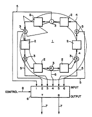
Fig. 2 shows a memory device that is capable of storing data; .. r.. ~, ;r,.~
i.e., titles of various sorts. The device is u~,~l of a plurality of data
storage devices 2, togetner forming a storage unit 1, and a plurality of l~ortals
3. The portals 3 are dispersed around the storage unit I in a manner that can beo described by means of modular ~rithmotir As indicated by the dilCI_liUI~
arrows ~ r~ on signal paths 4, the memory device is ~ d to
establish relative movement between data stored in the storage unit and the
portals 3.
Preferably, the storage devices 2 are arranged in the storage unit l in
series fashion to form a ~ .L.lill6 structure. This structure can taice tne formof an endless loop or ring, as shown in Fig. 2. Tne specific form chosen,
however, is not ~,~u L~ ulally important, as long as the structure is ~.lldlic and
provides a llcdi~ blc ~1 ~ of storage devices 2. Preferably, the
~o ~ of storage devices 2 is defined in accul.l~.~cc witn modular
~rithm.-tir Modular arithmetic will be explained below, in r ; t; with the
detailed ~iiCr-le~;~ln of tne portals 3.
13
W095132s05 2 1 9 1 1 1 ~ P~llu~ 39
Fig. 2 shows six storage devices 2 connected into the ring structure. (As
will become more apparent below, the number of storage devices 2 in an actual,
c~ bo~ would be far greater than this. Only six are shown in
order to render dcs~. r of the invention simpler and clearer.) As will be
discussed in ~ of various ~ c, below, the StOMge devices
2 can be selected from a wide variety of existir~g t ~ Ci ` Currently, the
most prefeMble hardware options are various types of ~ .. memory,
e.g., shift registers, delay lines, CCDs, RAMs, ROMs and non-volatile
memories of various types. Advances in ~ Oy will surely expand the list
o of available options.
The portals 3 are connected to the stoMge unit I at various locations. In
Fig. 2, the portals 3 are connected into the ring and alternate with stoMge
devices 2. However, as with the storage devices, the particular form of
- is not important to the invention. Rather, it is important that the
portals 3 are arranged in a systematic and ,,l~~ manner, and that they are
~io C;~ to allow data to enter or exit (or both enter and exit) the storage unit.
As noted above, the O of portals 3 is defined by modular
0 arithn~ti~ Modular - ' , as defined by Merriam-Webster Inc., is the
"arithmetic that deals with whole numbers where the numbers are replaced by
their ..,."u..~,. sftcr divi~i~n by a fixed numb." By w~y ~f e~ 1e, ~ince
W095J32505 ;~ 3 r~ c:l39
the hours in a day are also defined by a modular ~IrithnnPtir, 6 hours after 9
o'clock is 15 o'clock, but is also 3 o'clock, because clocks follow a m~dular
arithmetic with modulus 12. Stated in the form of an equation, the i..., .~.
- of portals 3 is defined as follows:
Pj ~ Pi IM ~
where Pj = any chosen data portal in the -~, t, and
M = the total number of data portals 3 provided in the storage
unit 1. Fig. 2 shows a storage unit provided with M = 6 data por~als 3.
(Again, a ~.UIII~ ' would most likely contain many more than
iX portals.) Thus, the seventh data portal 3 is equivalent to the first data portal
3.
The r~lstir~n~hir between ~., data portals can also be described
,, ~,1, ,. ,;. ~lly, as follows:
pj + f(t) = Pi+l,
where Pj = any chosen data portal in the .,.. ,. .
Pi+, = the next data portal relative to Pi, and
f(t) = a function of time. It should be noted that, given the non-
. .. 1;.. --, ~ nature of hardware ;, ~ ; f(t) should not be construed as
being limited to a smoothly function, but includes rational n,umber
(e.g., integer) c,~ ; .-l;rnc of ~ functions. ~f~l~ly~
f(t) = C,
W095/32505 2 ! 9 1 1 1 3 PCTIUS95106139
where C = a constant. When f(t) is constant, the portals 3 are arranged
around the storage unit I at fixed, regular intervals, as illustrated in Fig. 2. The
benefits of having constant intervals between portals include the ability to
construct the ring and, in particular, the portals, of pre-fr' ~, modular units
(other benefits are described later in the ~ \) The intervals need not be
constant, however, to provide an operable and practical memory device 1. For
escample, dispersing the portals 3 according to the function:
f(t) = log (t)
causes tbe intervals between portals to become P~ ;1C.~ ,ly longeruntil the loopo returns to the initial portal. The function:
f(t) = sin (t)
causes portals to bunch at various locations around the ring. Any other functionof time can be utilized, to match er~if -- desired by the service provider,
and thereby more closely match the r ' needs of end users.
Arranging the portals according to modular anthmetic renders access to
data stored in the memory device calculable and c~,-udu_il,l~. The benefits of
the systematic nature of the ~ will become apparent bdow.
The portals 3 shown in Fig. 2 are each co~.~l-uc~l as data IC~ dlUI~,
such that, if selected, each portal performs both a -,IJli~..li-~g and an outputting
function. This is indicated by the arrows shown on each of the signal paths 4
16
W095/32505 ;~l 9 1, l 13 1~ ,.,''C'139
and 5 ~ from each portal 3. The arrows on signal paths 4 indicale data
that continues .,u, ' " in the ring. The arrows on output signal paths S
indicate data which is output from the ring. This is the preferable ~f1l1G~
Alternatively, the memory device can be Cul~LI, ' with non-~eplicating l~ortals
3 and separate data l~r~i (not shown), which merely replicate the data
stored in the device 1 but do not output it from the ring. Examples of hardware
that can be used æ portals 3 include latches, logic gates, IC,~ and
..~
,o Although not specifically shown in Fig. 2, the memory device includes a
means which forces portals 3 and data stored in the storage unit 1 to move
relative to one another. C.~ y, it does not matter whether the data moves
and the portals remain static, or whether the portals move while the data l emain
static (or, for that matter, whether both the portals and the data move relative to
some third point of reference). The ~ e~-- shown in Fig. 2 is one in
which the data move and the por als 3 are fixed.
Generally, in digital ~ f,. ~ the means which establish the relative
1ll~.._lll~,ll~ would be embodied by some form of clocking ' T~rpes of
clocks eæily adapted to a memory device according to the present in~ention
include n-phase clocks, timing gPnPrPt~, address G ' , data ' i, 1
and llf;~lU~JlU~ U~
17
WO 95/3250~ 2 ~ 9 ~ I 1 3 PCT/US95/06139
Finally, Fig. 2 shows a controller 6 connected to the storage unit 1.
~pc~ fi~ ly, the controller 6 is connected via signal control lines to respective
portals 3. The controller 6 is cc,.~rl~;ul~i~ to control data traffic at the portals 3,
e.g., by selecting among dah portals 3 in accold.,~lcG with an externally supplied
control signal 8. Data traffic includes either the input of dah into the storageunit I via the portals, or the output of data from the storage unit 1 via the
portals. As such, the controller 6 ~ h ~ and regulates c~ between
the data portals 3 and signal lines 7. The signal lines 7 in Fig. 2 are indicated
by the arrows as being output lines that transport replicated data out from the
unit 1. However, the signal lines 7 can also be used for inputting data into theunit 1.
B. O~eration
In operation, the memory device is utilized for inputting data, for storing
data and for outputting dah. These three aspects will now be described in turn.
In an input operation, data to be stored is presented to some portal 3 in
the ring, e.g. portal number 1. Once the portal number 1 is activated, the dah
is fed into the storage unit via the portal number 1 preferably as a sequential data
stream. Any data IJl.,vh~u~ly existing in the ring is thereby over-written. The
input operation is completed when all of the data desired to be stored has entered
the storage unit I via the portal. Thus, for example, if one wishes to store data
18
21 91 1 1 3
WO95/3250!i P~ I/I ~'~!~139
cu~ ùr~ .g tû a movie title in the memor,v device, according to one
strai~;llLI;.-w~-l model, the data is input in serial fashion, starting wi~h thebeginning of the movie and ending with the data cu~ ù~dillg to the closing
- eredits. If desired, the data may be input in a time-division ,. il~ or
space-division '~' ' manner. This can be achieved, for example, by
selecting more than one portal, e.g., the portals numbered 1 and 4, at
t " ~ 1 relative times, for example, ~ ?u--~ly.
The controller 6 can, but need not, be used during the input opelration.
If the controller 6 is used, the controller 6 selects one of the signal lines 7 and
one of the portals 3, and controls the input of data from the selected line 7 to the
storage unit I via the selected portal 3. If the controller 6 is not used, an input
line is simply connected directly to one or more portals 3 during the input
operation.
Once the data is input, the ring stores it in a cyclical ~ g~ A
eyclical: - lg is one in which, even though, en route, the data may be
processed (e.g., error-corrected, error-proofed, ' ' ', encoded, decoded,
encrypted, decrypted, etc.), branched, diverted, or otherwise acted upon,
eventually, the data (or an z.~JlU~ facsimile or correlate thereof) and an
"~JIJI' r ' point (such as a portal) in the memory structure will again coincide.
Several variations are pûssible. For example, the point in the memory slructure
19
21 9 ~ ~ ~ 3
WO 95/32505 P~~ 139
may be stationary, while the data is kept in motion. Conversely, the data can
be held fixed while the point in the memory structure is moved. Also, both the
data and the points can be moved, relative to some third position of reference.
r ~ 6 each of the above variations will be described in greater
detail later in the sr- ~ ~~'
Fig. 2 shows a cyclical ~ In. c. ~ of stored data in which the data
moves relative to fixed portals 3. More specifically, the data circulates in a ring
structure, passing from one storage device 2 to the next, and so forth. If the
o portals 3 are connected into the ring, as shown in Fig. 2, they pass the datd from
one storage device 2 to the next during storage but otherwise remain passive.
llaii~l~,ly~ the portals 3, equally well, can be appended onto the ring, such
that, during storage, the data stream passes directly from one storage device 2
to the next without passing through the portals 3.
The fidelity of the stored data is ~ ' while the data circulates in
the ring. As such, the datd circulates in the same order in which it was input
into the ring. Thus, if the ring has been loaded with data ~,u~lca~ul11;1.6 to amovie title, the movie title datd circulates 1y through the ring, head
fohowing tail. As viewed from a specific point on the ring (e.g., some given
portal 3), the datd repeatedly passes by in the fashion in which it was loaded.
The rate of ~,uldLi~ is ~ by the frequency of the clock used by the
WO95132505 21 91 1 l 3 r~ C'139
memory device, as described above~ The clock can also be used to al~er the
rate of circulation, if desired. For instance, it may be desirable to provide an~UIa~ wherein the relative IIIV~ between the stored data and the data
- portals is il~t~ I.. rather than continual. A~ conduc;ve to
il.t.,.. ,.ilt~,lA data ~lu6l~ ;v~l include video games and electronic ca~:alogs.
Movies, television programs, music and the like are preferably stored using
continual ~I.e., ull.l~t~ ~t~,d) data ..v~.
When it is desired to output data that is stored in the memory clevice,
o first, one of the portals 3 is selected by the controller 6 as ~ d by the
control signal 8. Also, one of the signal lines 7 is selected as an outpllt line.
The output operation then ~ f~,lalJly proceeds by ~ ' ,, the stored data at
the selected portal and delivering the l~ lUdU~ data to the selected output line7, so that the data may be routed to an ~ ;dt~ ~ec~ otjon No further
control is needed; once the ~ r ' portal is selected and tbe output op~ration
" the stored data stream simply "flows outn, i.e., is I~IUdU~;I and
delivered as it passes the selected portal. The output rate simply matches the
rate of ~,il, ' of the data within the ring (assuming the portals operate at real
time). When the complete data stream has been output from beginning to end,
in ~ c, the controller 6 may sever the ~ . between
the selected portal 3 and the selected output line 7. Of course, during the
described operation, non-selected portals simply pass the data within the ring,
21
2~91 ~ l3
WO 95/32505 r~ ."'0~139
wivhout ~ -vJu~ ,S it, on to the next storage device 2, as described above.
The decision of which portal to select is governed by the IllUlll~.l~y,
current locavion of the stored data stream relative to the portals 3. For instance,
if the stored data represents a movie title or television program, and it is desired
to output it from its begirr~;r~ a portq~l is selected which lies an _~v,
distance dv .. Il~ ,r~ll of the current location of the beginning of the title/program.
The IllU...~,.lLll.y, current location can be ' ' 1, given the l,lcJi~
I of the portals around the ring and the known rate of circulation of
,0 the data (or 1 I ).
~rifirAA1ly~ given the described structure, it is possible to construct
V~ t; functions to calculate the portal to be accessed. Such functions,
which would be apparent to those skilled in the art, can determine the portal tobe accessed based, e.g., on the portal that was used to load the data, the time
elapsed from loading, and the speed Of ~ r ~ '' ûf the data. If, as described
above and as shown in Fig. 2, the intervals between portals are constant, i.e.,
f(t) = C, the rAlr~lq~irn is especially simple.
Of course, variations more . ,' ~ ' than the ones just described,
which utilize more complex ~ulr ~ of portals and/or data storage, are
possible. Such functions, even though more complex, ~ r~ operate
22
WO9S/32S0S ~ ~ 9 ~ ~ 1 3 1~l/l,L ~0~l39
according to the same principle, and are covered by the present inventioll.
The ability to compute a desired portal relative to data is a feature of the
invention which is not ~ ;r of outputs of standard electronic devices
(e.g., prior art shift registers, delay lines, CCDs, and so forth). As such, the
calculated portal number assumes a quality more . 'y associated ~ith an
Input/Output operation ~,.ru~ ,d by a computer. However, unlike an I/O
operation, a single c~ provides access to an entire stream of stored
data, not just one data unit. Further, the provision of plural data portals permits
o u . _~L~ ,i-.t output sequences not a~h;~,v~lc by standard I/O operations. F;nally,
this feature also ~ the present invention over known r ~
;.... systems, such as local area networks (LANs, e.g., Token Ring,
Ethernet), wide area networks (WANs), ...~ u~uLI~.. area networks (MANs),
and cable television systems. In these syskms, ' ' of a portal llas no
1~ ;r~ -~h l~ with input/output rJF~ti-~nc Rather, these systems require
~.ul~b~ U~ 5~ I t~ , ad-l~.,~;,;..~5 and routing schemes, to permit users ~o find
and access data in the system.
In a practical operation of the memory device, plural data portals would
normally be active in outputting data at any one time. Thus, in a lypical
operation, a first data portal 3 (e.g., data portal number 6) is select~d for
outputting the data at a first moment in time. The controller 6 controls the
23
WO9513250S ~ ~ 9 1 1 1 3 r~,l/u., 5.r 139
output such that the data is replicated and routed out from the storage unit 1, via
a first selected output line 7, to a desired first end-user ~r ~ I;r~l~ The selected
output line 7 thus carries the data, e.g., movie title, television program, etc., out
in its sequential order as a first data stream. Thereafter, if a second end-users ~ ;r)~ requests the same data, the controller 6 again calculates which portal
shou~d be selected for outputting the data at the second moment in time. The
controller 6 then replicates and routes the data as a second data strealn from the
second selected data portal (e.g., portal number 2), via a second output line 7,to the second end-user .1~ ;n.
If the above-describcd r~l ' '-n~ again happens to yield data por~al
number 6, preferably, the ' ' would provide for selecting the next
available portal, here portal number 1. Given the large number of portals and
short time delays betwcen portals in an actual ~.. ,1,~1;,.. ~, the end user would
s not perceive the resulting delay. For instance, in a working ~ .1.~.1;.. ~, the
time delay defining intervals betwcen cua3~ 1iv~ portals might be chosen to be,
e.g., anywhere between 5 minutes, the best estimate of current human patience,
and l/30th of a second, the current refresh ra~e between television frames. The
intervals between portals would be 1 ~ 1 primarily by balancing grade of
service with cost of the service.
Since the stored data is replicated at each selected portal, and the portals
24
W095132505 ~ q ~ ~ ~ 3 r~lm~,; 139
operate ;~ fl~f ~if ~ly~ there is no lc~lu;~ that output of the second data
stream be delayed until the first data stream has been CVIII~JL~i~IY output. In
other words, the data streams being output may be staggered, i.e., partially
overlap. As a result, in the ~ of Fig. 2, even though only one copy
of the title is stored in the unit 1, the title could be output to six different cnd-
user rif cti~ati,~nc at once if the porials were each activated one after another.
r, ~, the signal lines 7 may be controlled in such a way that one
given data stream branches to multiple end users. As such, the numbfr of
staggered "playbacks" of the stored title is further increased by providing
playback to different end-user rif ctiT~atil of any or all of the
staggered "~JI~,i~,~" .
As apparent from the r1 above, since the data stored inl the
memory device can be output as a large number of; 1~ IJ' .. 1. .. 1 output data
streams, the present invention provides an extremely powerful method of
accessing data. Further, since the data streams (accessed as described and
further cloned if desired) can be routeci to a y~ ly unlimited number of
, the present invention provides an extremely effficient method of data
. .
W095/32505 : 21 91 1 1 3 r~ .'C-139
C. Altern~ive Structures
The design of the memory device described above implies that digital
i- r...- ~;., Will be ~ d~ g in a loop and that portal locations are fixed at
given locations on the loop. According to the invention, however, it does not
matter whether the data moves and the portal location is static, or the portal
location moves and the data is static (or whether both move relative to a third
chosen location). All these &lL~IIdti~ designs perform the required f... ~ y
of a memory device.
As evident from the al~.ll~ s discussed below, the manner of storing
and accessing data (preferably ICI~lCD~ lil.æ video and/or audio il~l )
according to the present invention is amenable to a variety of designs. Figures
3 and 4A-4D inclusive illustrate the moving output ports (address) design.
Figures 2 and 5A-5D illustrate the moving data alternative. Figures 6 and 7A-
7D inclusive illustrate movement of both the ports and the data.
C1. First Alternative: Fixed Data, Moving Portals
Fig. 3 shows an alternative where the data forming a title 100 is held
fixed in time in a data memory. As shown, tbe title 100 is subdivided into
numerous individual blocks I to n and stored. Each block is a sequential
segment of data. Preferably, each block of data is associated with one portal
26
21 9 1 1 1 3
101. Fig. 3 also shows a control device 102, which is used to select data bl,~cks
by activating d~ JI idL~ portals 101.
During an output operation, the control device 102 activates the portal
s 101 associated with data block 1. The data in block I travels via sigmal line 103
to the control device 102, which transfers data block I to arl output line 104.
When data block I has been sll~c~ccfi~lly output, the control device 102 will
cause the next portal 101 in the sequence to be read. In this case, it is the portal
associated with block 2. In this manner, the control device will activate one
o portal after another, such that the output portal being activated changes ~-ith
time. As such, the data stored in the data memory is held fixed, while the portals
used for accessing the title data move.
In more concrete temms, Figs. 4A-4D show an imrlement~tion of the fxed
data, moving portals altemative. Figure 4A depicts a group of "N" memones
110. Each memory has a capacity of eight cells (a cell being any arbitrary
amount of data). The configuration of data relative to output port I ~see
reference number 111), shown in figure 4A7 ~,u~ d~ to a reading operation
of the data Dl held in the first cell of the first memory 1. Figure 4B shows theresults as the second piece of data D2 held in the second cell of memory I is
being read. This process continues until the data D8 in the eighth cell of memory
I is read, as shown in Fig. 4C. Before the next piece of data is n ad,
27 AMENDED SHEET
the "pointer" in the column of cells is then reset to the position associated with
the first cell. Additionally the output port 1 is moved to the "next" memory 2.
This is shown in Fig. 4D. This process continues until the full data stream has
been accessed and output. Once the "last" piece of data is output, the output
port 1 is again free to be reset to the initial memory cell location and to
commence reading the data stream D1-DN from the beginning. If the memory
structure is fully utilized, the "last" piece of data DN should be stored in cell
number 8 of memory N. However, the "last" piece of data may be held in some
previous location in memory, for instance, cell 3 of memory N-1.
Referring back to Fig. 3, the control device operates according to a
programmed sequence defining the sequence in which the portals 101 are
accessed. This programmed sequence can be determined by an external control
signal 105 or can be stored internally in the control device itself. If stored
internally, the external control signal 105 may still be used, e.g., for selecting
between several different stored sequence programs.
The data memory used in this alternative can be any of a number of
memory storage devices including dynamic RAM, static RAM, and pseudo static
RAM. Further, there is no limit on the size of a data block. For example, one
data block, as shown in the figure, can represent a completer RAM, a sector in
RAM or even just a bit. The portals 101 can be constructed from logic gates,
28
~191~
.
gate arrays, programrnable logic arrays, etc. The control dev,ice 102 can be made
from a number of devices including logic gates, gate arrays, mi~lu~ JC~ul~,
and sequencers.
s C2. Second Altemative: Moving Data, Fixed Portals
In illustrating the principle of the invention, Fig. 2 showed one memory
arrangement in which moving data is accessed by fixed portals. Figs. SA-SD
show one possible implementation of the moving data, fixed portals altemative.
Figure 5A shows the configuration of title data I I S relative to output port I (see
o reference numeral 116) when the data D1 held in the first cell of the firstmemory I is being output After the first piece of data Dl is read, the data D 1-DN are transferred, as shown in figure SB, such that the ne~t piece of data D2
can be read. Figure SC shows the data position once eight read operations have
occurred. Figure SD shows the relative position of the data to the output port I~5 while DN, the final piece of data in the data stream, is being read.
C3. Third Altemative: Moving Data, Moving Portals
Fig. 6 shows an altemative where the data fomming titles 120 and 130 are
moYing in time in respective data memories. The title 120, subdiYided into
~o blocks I to n, moves in time much in the same manner as described with respect
to Fig. 2. In other words, the data blocks moYe from one storage sub-unit to lhenext. The title 130, also subdivided into blocks I to n, moves in time wit~lin
AMENDED SHEET
29
W095/32505 2 ~ 9 ~ I 1 3 P~,l/u.,,~ 39
individual storage sub-units. Such an Al 1~ would exist, for example, if
each storage sub-unit were LU~ ULlCd of a ~ LUldling shift register, as
described with respect to Fig. lB. The allal.6~ l1 of Fig. 6 is shown with one
portal 121 or 131 associated with each block of data stored in the respective data
rn^mnri~
During an output operation of the title 120, the control device 122
activates the portal 121 associated with data block I of that title. The data in
block 1 travels via signal line 123 to the control device læ, which transfers data
block 1 to an output line 124. When the data block 1 has been ~,ol~l~k,t~ly
output, the control device læ will cause the next portal 121 in the ~JIV~;""'' I '' ~
output sequence to be read. In this manner, the control device will activate one
portal after another, such that the output portal being activated changes with
time. Since the data blocks forming title 120 are also moving, the location of
the data blocks also changes with time.
In more concrete ter!ns, Figs. 7A-7D show one possible ~ ;o l
of the moving data, moving portals ~1~ v~,. Here, output port I (see
reference numeral 141) is always associated with memory 1. Figure 7A shows
~o the c~ ~, of title data 140 relative to output port I when the data D1 held
in the first cell of the first memory I is being output. After the first piece of
data Dl is read, the data Dl, D9, D17...DN are llall~rl~llLd as shown in Figure
woss/32sos 2 ~ 3 r~ s,,~c-l39
.
7B. The "pointer" is moved to the next memory cell in the same memory 1, to
read data block D2. Figure 7C shows the data position after eight read
op~tin~ cu~ Julld;l.5 to Dl-D8, have occurred, and the "pointer" has
moved ~,ulll~L,t~,ly up the column of cells of memory 1. Figure 7D sho~s the
device during the next ~ 'læ i read operation. Here, the "pointer" is reset
to the bottom of the column of data cells of memory 1. Also, by this time, the
data forming title 120 has been completely shifted over by one memory. Thus,
e.g., the data formerly held in memory 2 is shifted into memory 1, and the data
formerly held in memory 1 is shifted into memory N. The "pointer" now ~egins
o reading up the column of memory 1 once again, but now reads the next set ofdata D9-D16. This process continues until the data Dl finally returns to
memory 1.
Returning to Fig. 6, an output operation of title 130 proceeds as described
with respect to Figs. 4A4D. However, here, data blocks 1 to n are moved
internaUy within individual storage sub-units. Thus, according to one concrete
example (not illustrated), data stack Dl-D8 circulates within memory ], datd
stack D9-D16 circulates within memory 2, and so forth.
The data memory in this third alternative can be cu.. ~ ,t~,d, e.g., of
uuldLI~g shift registers, charge coupled devices, or RAM controlled by data
and the like. The control device can be; ~ t d through
31
woss/32~0~ 21 91 1 1 3 r~ .o~l3s
JIUI~ l, data se-lu~ , logic gates, gate arrays, etc.
II. SPECIFIC EMBODIMENTS OF I~IE INVENTION
As evident from the r~ discussed below, the hardware
design options for storing and accessing data according to the present inventioncdn be chosen from a variety of existing ~ o;- c Currently, the most
preferable memory device hardware options are various types of Sf ~
memory. Advances in ~ ' ' Oy will surely expand the list of available
o options.
A. F*st E: ~,,.1;,. ..1 Shift Re~isters
The preferred manner of e..ll.ody;l~O a memory device using shift registers
t5 iS shown in Fig. 8A. Fig. 8A shows a long series of clocked shift registers 151
connected to form a ring 150. The ring 150 is c~ .lu.,t~d such that an entire
title is capable of being stored on the ring. Typically, to store a two-hour
movie, using MPEG2 as a data CUIIIIJICj.~;Un method, the ring should be able to
store ~ 'y 180Gbits. The ring 150 is clocked by a clock source 152
which governs the rate of ~dl~,uld~ n of the data around the ring. The ring 150
is preferably clocked at such a rdte to deliver (i.e., output) the title at a rate
required by the receiver.
32
219~1~3
wo ss/32sos ` r~ c -l3s
If the clock rate required cannot be attsined by one shift register, many
registers in parallel can be used to obtain the rate required. Fig. 8B illust]rates
one possible such ~ ' ~ in which two parallel rings are cu~ lu~ l, each
L clocked shih registers lSI connected in series. Fig. 8C illustrates
an ~l.~l................... ~ in which shih registers 151 are ~ in series and in
parallel to form the ring IS0. The rate required is ~ largely by the
. imposed by the service provider.
The data forming the title pæses through the shih registers 151 serially
o as a sequential bit stream. The data is passed from one register lSI to the next
in a manner explained in greater detail below.
The access to the title stored in the ring 150 is obtained via the data ports
153. An example of a port 153, coupled between two registers 151, is shown
~5 in Fig. 8D. As illustrated there, the pûrts 153 are preferably composed of logic
circuitry 160-162. In addition to an input connected to the registe]r lS1
preceding it, each port 153 hæ an input for receiving a bit stream input 154.
Data for a new title is inserted into the ring 150 via inputs 154. In addition to
an output connected to the following register 151, each port 153 also ~læ an
output 155 for copying the bit stream ~ ,uld~ 6 in the ring 150. The mlmber
(spacing) of ports 153 included in the ring 150 is bæed on an efficiency
..A~;nn, balancing overall cost against access time. The spacing of the
33
1 1 3
ports 154 defines the time intervals bet~veen permissible data access, and thus
determines, in part, the waiting time between a subscriber request and
fulfillment. If the title is accessible in sufficiently small increments, the delay
time is i~ by humans.
s
The embodiment of Fig. 8D, described above, has no provision for error
correction between registers. As shown in Fig. 8A, ~,c;llcl~lL~ 156 ca3l be
inserted periodically in the ring 150 such that the data stream stored in the ril1g is
~;g~-l.,.d~d as it passes through the regenerator. Fig. 8E shows in greater detail
an embodiment in which the 1~ d~11 156 is formed as a data checker 156'
inserted between the registers 151. Each data checker 156' preferably contains
logic circuitry 163-165 as well as a decoder 166 and an encoder 167. These are
preferably a Reed-Solomon decoder and a Reed-Solomon encoder, respecti vely.
The decoder 166 receives the data stream at an input, outputs any errors detected
via an output 1, and outputs the decoded data to the logic circuit3y 163-165. The
output 168 leads to operational surveillance units. Similarly, the data stream is
input into the encoder 167 and is output as an encoded data stream to the next
following shift register 151. Regeneration occurs as the bit stream passes
through the Reed-Solomon decoders/encoders. Thus, errors can be corrected
and/or brought to the attention of surveillance ,~ lirmPnt
AMEND~D S~IEET
34
wo9s/32s0s ~ 91 1 1 3 ~ 39
In addition to error correction, stored data can be processed in other
useful ways known to those skilled in the art. Thus, for example, data can be
encoded or encrypted. Data would be encoded to provide means to ensllre its
reliability and to facilitate access to it. Data would be encrypted to prevent
~ access to and use of the data.
Further, data may be cu..,l,l,,i.,.,d. r~L;l~ulculy with respect to video
r '-~, the repetitive data content of video signals allows for significant
reduction in required data storage capacity by use of ~UII.~!JICSj;U.~ schemes.
o Such schemes include MPEG, fractal and variable data rate coding. M[PEG,
currently the most common scheme used in the t~' indlustry,
uses a discrete cosine transform and is a lossy . . ci..;Ol~ scheme. ~PEG
provides a ~ D~;UII ratio of .I~ u~dl~dt~ly 38:1. Fractal CVII~JIC;.:,;O.
c which have only recently become viable, typically provide
CUI~I~JIC;I~ I. ratios of .. ~., 1~ 1500:1. References describing image
,;. .;û~ t~ 1 c include W.B r. ~ et al., JPEG (Reinhold, New
York, NY, 1993); M.F. Barnsley et al., FrAr~l Tm~ Cu..~ ' (A.K.
Peters, Wellesley, MA 1993); Chiang et al. "Hi.,.~l.;.,~l Coding of ]~igital
Television", TFFF. Ci ~i ~A7in~ Vol 32, No. S (May 1994), pp.
3845; Pancha et al. "MPEG Coding for Variable Bit Rate Video Tl ",
!FFF C~ C M~A7;n~ VOI. 32, No. 5 (May 1994), pp. 54-66.
WO 95/32505 - 21 9 ~ ~ ~ 3 PCT/US95/06139
The ~.. I....l . c of encoding, ~ JL~g and data CU---IJIC;~;U~ just
described can be a.lv~ y ;~u~ul~-t~d into the methods of storing data
described in the present d~ ;l. Thus, if the data stored in the ring is
encoded, it can be more efficiently accessed and more reliably stored. By
~ y~Ll.g the data, ûne prûvides added security against ~ 1 .. ;, ;1 access to
and use of the stored data. Finally, data ~ , ~ provides ~i~nifirs~lt
savings in hardware costs, since the storage rings can be Cu~lstl 1 ' ' of far fewer
o As such, each ring is structured to allow data to be placed into the ring
and copied from the ring. Further, each ring is able to detect and repair errors
'1~,. If excessive errors arise, this fact is signalled to the surveillance
, . t, such that the ring can be taken t~ Julal;ly out of service and
repaired.
The details of cu~ m of the circuitry of the ring 150 are not
~L~.ul~uly important in the present invention. The shift registers 151 can be
~;u~ u~t~l simply of standard logic circuits. The logic family for ~ n
of shift registers includes Emitter Coupled Logic (ECL), Transistor Transistor
Logic CITL), and Metal Oxide '` ' (MOS). The logic family and the
ululdll~db, memory size of the shif~t register are shown in the table below.
wo95/32s05 2 1 9 1 1 1 ~ r~1~9
Shift Register T~ o~l Memory Sizes
Logic Family Size In Bits
ECL 512
TTL 1,024
MOS 1,048,576
A memory device according to the first preferred ~ ...1.~.1;..,...: may be
,' ' through the utilization of off-the-shelf shift registers. For the
o purpose of storing and accessing movies and the like, the MOS-type shift register
is preferred, due to its larger memory size.
The above c .. I,odi.. ~ is an example of a memory device in whilch the
data portals are fixed and the stored data stream is moved through the shift
registers 151 and through the data portals 153.
B. Second E.,.~. .l;,... - ~ ('h~e Coupled Devices
A further, preferred alternative for ~..I-bOd~J;I.o~ the memory devicl~ is to
employ CCDs 171 (Charge-Coupled Devices) as the registers 151, as shown in
Fig. 9, to form a ring memory device 170. If the ring 170 is C()~allb_L~,d usingCCDs 171, then each CCD 171 must be pumped by a clock source 172.
37
wo ss/32sos 2 1 9 ~ 1 1 3 r~ s~ s c l39
Further, some form of Ic~ ~f ~ e means 176 must be coupled between eachCCD 171. T~ ;, for the Ic~ aLllg means 176 include logic gates, as
above. The individual CCDs simply function as registers in this ( ..~Jo~ f l~
and the ring memory device 170, overall, functions similarly to the ring memory
device 150 described with reference to Flg. 8.
C. Th;rd E~ l;" . .,~ Delay T inf ~
A further ;, ~ ;ù-~ of a ring memory device, using delay lines 181
o as the storage devices, is shown in Fig. 10. Access gates 182 connect the
individual delay lines 1~1 together: Preferably, the access gates 182 provide
data ingress lines 183, data egress lines 184 and access control lines 185. The
delay lines 181 ~ IDCI~D are preferably provided with egress ports 186 in
addition to those provided at the access gates. In operation, signals Lla..DIIl;lt~
over the access control lines 185 activate the ingress lines 183 or the egress lines
184, thereby allowing data to be input to or output from the ring memory device
180, ICD~ ,1Y. If it is desired to output the title via one or more of the
additional egress ports 186, a~lu.ul gates at ends of the egress ports 186 arecontrolled a~cu~.l;l.61y. Otherwise, operation is analogous to that described with
respect to Fig. 8.
38
woss/32sos ~ 9 ~ ~ 1 3 F~I/~ 39
D. Fo~rth El"bo~ . Random Access Memories
- Fig. 11 shows yet another . . . 1 .u. l; . . -- .l of the invention; which utilizes one
or more random access memories (RAM) to store the data COI~G;I~lUlldill~ to a
title. As shown, a RAM 190 has a series of address lines Ao - AN~ a dala line
Do~ and a read/write line R/W. The RAM 190 is connected to a data seq~lencer
191 ûn the one hand and a control device 192 on the other hand. In operation,
the data sequencer 191 cycles through the address lines Ao - AN in dccùldc-l~
with a clock signal input to the data sequencer 191. At the same time, the
o control device 192 activates the RAM 190 by triggering the line R/W and thedata line Do. As a result, the data ~UIIGi~l.1U~ldill~6 to the title stored in the RAM
190 is output in sequential order on the Data Out line. Various alt~,l,ldLi~ fordesigning an ~ ."~ utilizing RAM have been described with reference to
Figs. 3-7D, which need not be repeated here.
I~ .
There are various types of RAM currently on the market which could be
used to .' a memory structure as just described. These include Static
Random Access Memory (SRAM), Dynamic Random Access Memory (DRAM),
and Pseudo Static Random Access Memory (PSRAM). Digital r -t)n
stored in SRAM is held in "static" locations. Several transistors are requlired to
form a memory cell that represents a binary digit. In order to store 1 million
bits of data, a device would need several million transistors. This packing
39
W095/32505 2 ~ 91 ~ ~ 3 ~ .. .r~l3s
density is a~ ~lc today. With respect to DRAM ~ logy, the memory
capacity of DRAM devices has dramatically risen over the years. In fact, the
memory capacity has attained a level such that construction of a memory device
aeeording to the present invention ean be aehieved readily, using off-the-shelf
C~ J~ t~ DRAMs require periodie refresh of the data. The periodie
refreshing must be l~ . r.,....~ ~ on a constant basis. As DRAM technology is
widely used in the computer industry today, the cost is relatively low in
C~ to other ~ ' 'oO The elass of PSRAM memory is a relatively
new teehnology. PSRAM ~ represents a ~ ' -- of the benefits
o of SRAM and DRAM teehnology. PSRAM deviees have the memory eapaeity
of DRAM deviees, yet have an internal refresh eapability, rnal~ing them easy to
use. Advances in; ' '-O~ will surely provide additional memory options
suited to the present invention.
E. F;~h E"~ Stora~ge Medium Confinin~ Waves
Fig. 12 shows an ~ of the invention whieh is . u~ d
without the use of individual storage devices. Instead, the memory storage
device utilizes a memory storage medium 200 capable of confining cyelically
~JIU~ illg data.
More speeifieally, the data IC~JIC ' ~ one or more titles, or a portion
-
~1 9 1 I 1 3
O gS/325115 ~ 39
tnereof, is embodied in the form of a ~JIvp~.6dlill~, wave, where the wave defines
the stream of data. In the ~ ~.Lvdi~ shown, the storage medium forms a ring
structure, and the wave travels in a circle. The plu~d~d~i-.g wave can, in theory,
be chosen from any known wave ~ , e.g., sound, electro-magnetic
waves including light, ' u a~ and radio waves, but, preferably llight or
u..<.~, are employed. As known, such waves can be used to store
il,rul",d,iull content Further, such waves, when trapped in a cavity, h;lve the
property that they will sustain forward motiion. These properties of wa~es can
thus be used to provide data memory for the present invention.
As shown in the figure, a wave 201 ,cl,rt,;,~,.,L,.6 data is trapped in a ring
cavity 202. The speed of ~Jlv~J..6dlion is ~ t---; d by the imherent
of the wave and the medium chosen. The type of storage medium
chosen is ~ f~ .~lly one which minimizes ~IVlJ~6d~iO~ losses. Alt~ ,l.d~ ly, or
in addition, the storage medium may be provided with repeaters or other
. ' f~,;..g means (not shown) which ~ , for any l!lU~r~6d~iùl~ losses.
The list of currently available media for providing such a ring cavity 202 include
electrical cable, coaxial cable, ,c~,.b~. lines, delay lines, fiber-optical cable
andll~l~lv..a~ cavities.
~o
The ring cavity 202 is associated with a plurality of data porlals 203
sy~f~tir~lly arranged around the periphery of the ring 200. As discllssed in
41
wo 9sl32s0s 2 ~ 9 ' 1 7 3 r~ r c l39
the ~i~Srrirtinn of the principle of the invention, the systematic ~1 ,~ of
porLals 203 is one defined by modular ~nthrn~ic The ~ di~ llL illustrated
has five data portals, with intervals between C~1.3f~uiiv~ portals being equal
(although, a ";al f l~ would generally contain a far greater
number of portals). Individual porLals can be ~ either for inputting
data, or outputting data, or both. In practice, depending upon the choice of
storage medium, portals can be ~ LI~ tcd of ~mrlifif~ ,~g~ beam
splitter3, lllh ~ , cavity taps, and coa~ial cable taps.
o In oreration, a controller (not shown) is used to select one or more of theportals 203. When selected for data output, a given portal 203 passes the data
circulating in the storage medium, in the sequence and at the rate the data
appears at the portal. The data output travels along an ~lU~ t~, exit signal
line 204, to be processed and routed to it3 eventual l~ If the portals are
,LI~ ~ from one of the options listed above, their output is a copy of the
data cil, uL.L,,g, so that the data wave remains ~ ul~Lill6 in the ring cavity after
output. When data output at a selected portal is complete, the controller may,
in cl~ . instances, close the portal, so that no further data exit3 therefrom.
F. ~isth F --' ~ ' Stor~-f Device Coupled to Output Controller
Fig. 13 shows a memory device with further details regarding portal
42
. . .
21 9~
wo 95132~05 r~ tl3s
selection. This ....1)~ll;.,....l is again an example of a memory device 300
provided with a plurality of fixed access portals 301-305 and with a cap~bility
- of storing a moving data stream. Data can be placed into the device 300 or
copied out, as required. The present discussion will focus on data output. The
internal portals 301-305 are connected to a controller 310, with each portal 301-
305 being associated with one input 311-314 to the controller 310. The
controller 310 provides the selection and switching operability required to output
the stored data stream to external signal lines, via output points 351-352.
o More specifically, logic circuitry, including AND gates 321-328 a~d OR
gates 331-332, connects the controller inputs 311-314 to the controller output
points 351-352. Each AND gate 321-328 has a first input ~ A~ 2 at the
input 311-314 and a second input c-. ~ g a selection line from one of a
group of selectors 341-348. Further, each AND gate 321-328 has one output
line that forms an input into one of the OR gates 331-332. As shown, each OR
gate 331-332 receives inputs from a number of AND gates 321-328. The
number of AND gates 321-328 and the number of OR gates 331-332 is
d by the number of desired controller inputs 311-314 and desired
controller output points 351-352, as shown.
In a given output operation, a signal from a given selector, e.g., 341,
triggers a CUII~ JOlldillg AND gate 321. The activated AND gate 321 then
43
woss/32sos 2 t 9 1 1 ~ 3 P~ ..'139
permits the data stream from its associated output portal 301 to pass through
The selection signal 341 is chosen to ~y~ u.~ with the ~ ul~ 6 data
stream. Thus, if the title is to be output from its b~ginning, the portal is selected
to be able to "capture" the data stream from its beginning. (If title playback is
to . from some other point, e.g., after a pause operation, the portal is
again selected ~c ,..l;. L,ly to ~capture" the data stream from the other point.)
Then, the data stream flows out from the portal 301 and through the al~ul~ r
AND gate 321. The data stream then appears at the cull~,*,u..dil.6 input to one
of the OR gates 331, where it is passed through to the controller output point
o 351.
Either " _ 1~, or at any time thereafter, a second selection signal
can prompt a second output operation. Thus, for example, in a L'
output operation (or one c~ r~ ,g to the modulus of the ring), a second
s AND gate 325 that is connected to the same portal 301 as the one activated in
the first output operation is triggered by a further selection signal 345 to forward
the data stream. On the other hand, in an output operation occurring later in
time but before the first output operation is cnmrl~t~1 a second AND gate, e.g.,
327, connected to a different portal, e.g., 303, is activated by a selection signal,
e.g., 347. As in the first output operation, the choice of the AND gate 327 and
the portal 303 is 1~ " '\f3 by the ~ location of the starting point of
the data stream in the ring 300.
44
21 9 1 ~ 1 3
woss/32sos ~ r~ c ~39
Given a sufficient number of portals 301-305 and output points 351-352,
the data stream stored in the memory 300 can be output to multiple 1P~I;, -:;,,.,~
in a multi-u~ manner. Overlaps, as just described, can eitller be
complete or be partial. Fig. 14 illustrates one output scenario. As shown,
5 requests from ~.. 1.~ .;1.. ~ A, B and C give rise to " ,' 1y
U..~ .6, response outputs. Only one output portal, e.g., 301, n~ ed be
activated to respond to these three requests. The request from subscriber D is
somewhat delayed in time, however, so that the ~ -, . response output is
staggered relative to the response for ,.~1.,..;1....~ A, B and C. ThlJS~ the
o controller 310 selects a different portal in the ring to respond to the request from
D. Requests from additional ~ X, Y and Z are handled in
like manner.
In summary, the various data storage systems disclosed allow a wide
~:~u~ of titles (e.g., movies, æ ~ -, consumer-, and
business-related ;..rl.,. ~;.. ~ and any r nn that can be converte~l into a
stream of data) to be stored and retrieved by a wide audience witll great
flexibility and minimal contention between users for the titles offered.
The above ~ ;" Of the preferred ~ has been given by
way of example. From the disclosure given, those skilled in the art will not only
..... 1.. ~1~.. 1 tbe present invention and its attendant a l~ ~ but will also find
W095/32505 2 ~ 9 1 1 1 3 E~ 0~139
apparent various changes and ...~ that can be made to the methods and--
structures disclosed. It is sought, therefore, to cover all such changes and
- "~ as fall within the spirit and scope of the invention, as defined by
the appended claims, and ~lui~.,l.,..~ thereof.
46