Note: Descriptions are shown in the official language in which they were submitted.
WO 95/34890 P~1/lJ.. ,~. 'S,,
2 ~ 9 ~ 240
DESCRIPTION = =
DNA OPTICAL STORAGE
Field of the Invention
This invention relates to information storage devic-
5 es. More particularly, it relates to the use of syntheticDNA polymers for information storage in memory, most
particularly secondary optical storage mass memory.
Backr~round of the Invention
~Iistorically, data processing engines have been
10 physically and conceptually separated from the memory
which stores the data and program ~q. As processor
speed has increased over time, there has been a rr/ntinllrus
press for larger memories and faster access. Recent
advances in processor speed have caused system bottlenecks
15 in access to memory. This restriction is critical because
delays in obtaining instructions or data may cause signif-
icant processor wait time, resulting in loss of valuable
processing time.
Various approaches have been taken to solve these
20 concerns. Generally, the solutions include using various
types of memory which have dif f erent attributes . For
example, it is common to use a relatively small amount of
fast, and typically expensive, memory directly associated
with the processor units, typically called cache memory.
25 Additionally, larger capacity, but generally slower,
memory such as DRAM or SRAM is associated with the CPU.
This int~rm~l; Ate memory is often large enough for a small
number of current applications, but not large enough to
ho~ld all system LJL~JyLal.l.. and data. Mass storage memory,
30 which is ordinary very large, but relatively inexpensive,
is relatively slow. While advances have been continually
made in improving the size and speed of all types of
memory, and generally reducing the cost per bit of memory,
there remains a substantial need especially to serve yet
35 faster processors.
WO 9s/34890 2 1 9 1 2 4 r~
For the last 20 years most mass ~torage devices have
utili7ed a rotating memory medium. Magnetic media have
been used for both "floppy" (~lexible) disks or "hard~
disk drives. Information is stored by the presence or
5 absence of magnetization at defined physical locations on
the disk. Ordinarily, magnetic media are "read-write~
memories in that the memory may be both written to and
read from by the system. Data is written to or read from
the disk by heads placed close to the surface of the disk.
A more recent dev~o~ L t in rotating mass storage
media are the optical media. Compact disks are read only
memory in which the presence. or absence of physical
deformations in the disk indicates the data. The informa-
tion is read by use of a focused laser beam, in which the
15 change in reflectance properties from the disk indicate
the data states. Also in the optical realm are various
optical memories which utilize magneto optic properties in
the writing and reading of data. These disks are both
read only, write once read many ("WORM") drives and
20 multiple read-wrlte memories. Generally, optical media
have proved to have a larger storage capacity, but higher
costs per bit and limited write ability, as compared with
magnetic media.
Several proposals have been made for using polymers
25 for electronic based molecular memories. For example,
Hopfield, J.J., Onuchic, J.N. and Beratan, D.~., "A
Molecular Shift Register", Science, 241, p. 817, 1988,
discloses a polymer based shift register memory which
incorporates charge transfer groups. Other workers have
30 proposed an electronic based DNA memory (see Robinson et
al, "The Design of a Biochip: A Self-As~ ;ng Molecular-
Scale Memory Device", Protein Enq;n~erinq, 1:295-300
(1987) ) . In this case, DNA is used with electron conduct-
ing polymers for~a= molecular memory device. Both concepts
3 5 f or these molecular electronic memories do not provide a
viable mechanism for inputting data (write) and for
outputting data ~read).
W0 95/34890 E~ 5~
21 9~ 24~
Molecular electronic memories have been particularly
disappointing in their practical re6ults. While proposals
have been made, and minimal existence proofs performed,
generally these systems have not been converted to
commercial reality. Further, a specific deficiency of the
system described above is that a sequential memory is
typically subst~nt;~lly slower than a random access memory
f or use in most systems .
The optical memories described above suffer from the
particular problem of requiring use of optical systems
which are diffraction limited. This imposes size restric-
tions upon the minimum size of a data bit, thereby limit-
ing memory density. This is an inherent limit in systems
which store a single bit of data at a given physical
memory location.
Further, in all optical memory systems described
above, the information is stored on a bit-by-bit basis,
such that only a single bit of data is obtained by access-
ing a giving physical location in memory. ~hile word-wide
memory access systems do exist, generally they store but
a single bit of information at a given location, thereby
requiring substantially the same amount of physical memory
space whether accessed in a bit manner or word-wide
manner .
While systems have generally increased in speed and
storage density, and decreased in cost per bit, there
remains a clear gap at present between processor speed and
system requirements. See generally, "New Memory Architec-
tures to soost Performance", Tom R. E~alfhill, Byte, July,
1993, pp 86 and 87. Despite the general desirability of
memories which are faster, denser and cheaper per bit, and
the specific critical need for mass memory which can meet
the demands of modern day processor systems speed, no
completely satisfactory solution has been advanced hereto-
fore. The fl~n~A~Pnt~l limitations on the currently
existing paradigms cannot be overcome by evolutionary
W0 9s/34890 2 1 9 1 2 4 0 P~
.
Pnhiqnccr~ntq in those systems. This invention con6titutes
a new memory paradigm.
Summarv of the Invention
Synthetic DNA polymers are used as an optical storage
5 media for memory.- In the preferred ' - '; --t, a three-
dimensional memory is formed having three spatial dimen-
aions . Multiple ~= bit information is read as different
color wavelengths of light emitted through diffraction
limited optical portals on the surface of the media.
Structurally, a planar substrate (x-y dimension) has
multiple, physically separate read portals or read loca-
tions disposed upon its surface. In the preferred embodi-
ment, the substrate is disk shaped and the read portals
are arranged in radial tracks or on a decreasing radius
spiral around the center of the substrate. The read
portal is that area which will be ;ll~lm;n~ted by a read
illumination source to provide output from the memory.
The read portal cnnt~;nq within it one or more DNA
chromophoric memory units . In the pref erred erbodiment,
each DNA cl~ hnric memory unit is composed of a DNA
template, onto which are attached donor and acceptor
units. Functinn~l; 7efl DNA polymers have various arrange-
ments of cll~ nric donors, chromophoric acceptors and
~uenchers. The quenchers are associated with the donor
and/or the acceptor. The f~lnctinn~l ized DNA polymers
cont~;n;ng the donor/acceptor/~lPn~-hpr groups are arranged
on the planar surface of the media so as to project into
the z-spatial .1; q; nn . The chromophoric memory unit is
attached to the substrate.
To write~ to the memory, the response properties of
the chromophoric memory unit are changed. In the pre-
ferred Pmhntl; -t, a photochemical reaction destroys or
inactivates the s~uencher. A write source serves as the
illumination source for the photochemical reaction. In
the preferred embodiment, the ~uencher may be inactivated
by light, most preferably W light, and is formed with
WO95/34890 21 ~ ~ 24 0 r~
.
photocleavable linkers, or by derivitization of
chromophore molecules with photoactive groups. Thus, the
basic memory information is determined by whether the
quencher is active or not.
To read from the memory, preferably a single wave-
length light i8 used to illuminate the read portal. A
read illumination source illllm;nAt~R the read portal,
including the various chromophoric memory units rrnt~inA~
within the portal, providing excitation illumination to
the donor units in the chromophoric memory units. If the
quencher is not active, the chromophoric memory unit, via
the acceptor, radiates to the read detector. However, if
the quencher is active, no output occurs. In this way,
all chromophoric memory units in a read portal may be
simultaneously probed. If multiple chromophoric memory
units having various output wavelengths or other detect-
able parameters are included within a read portal, a
multiple bit or word-wide output may be obtained from a
diffraction limited read portal.
In the preferred embodiment, the chromophoric memory
unit utiiizes energy transfer between the donor and
acceptor, via the Forster energy transfer mc~rh;ln;~
Forster energy transfer is a non-radiative energy transfer
-n-h-n; P- which utilizes dipole-dipole coupling. The
energy transfer m~rhzln; Rm allows a single wavelength of
light to excite all acceptor chromophores.
In one embodiment, multiple write wavelengths are
used to selectively activate or deactivate separate
wavelength sensitive quenchers. If multiple wavelength
sensitive quenchers are utilized, the various chromophoric
memory units located within a given read portal may have
various chromophoric responses. Multiple write wave-
lengths may then be selectively used to activate or
inactivate quenchers. Upon illumination from the read
35 illumination source, those chromophoric memory units whose
output is not quenched will provide multiple wavelength
output to the read detector. However, those chromophoric
wt~ 9~34890 r~
2191240
memory units whose output is quenched will not provide
output .
In another l~mho~;r-nt, the read or optical portal is
further spatially subdivided (x-y dimension) into multiple
write sublocations. Each write sublocation is written to
separately from the other write sublocations in a read
portal . In the pref erred embodiment, a given write
sublocation contains chromophoric memory units whose
primary output wavelength i~ spectrally resolvable as
compared to the output from other write sublocations. By
writing separately to the individual write sublocations,
a single quencher material may be used for multiple read
wavelengths .
In another aspect of this invention, the output of
the read wavele~gth irom the write sublocation may be
varied. In the preferred e~bodiment, small wavelength
shift 6ubstrates, various intensity states and/or polar-
ization states may be affected by the use of multiple
~uenchers activated by different write wavelengths. By
way of example, uf;l;~;n~ a read portal of approximately
1 micron' 16 separate write sublocations may be formed.
Utilizing separate ~ pllnric acceptors for each of the
write sublocations results in a 16 bit wide word output
from the read portal. IJt;l;z;n~ one of the variations of
wavelength shif t substrates, intensity states and/or
polarization states can directly produce a 64 bit wide
word from a single sub-micron sized or diffraction limited
read portal.
Accordingly, it is an object of this invention to
3 0 provide an improYed mass storage system .
It is yet a further object of this invention to
provide a mass storage system with word-wide data output
from a single potentially diffraction limited read loca-
tion .
It is yet a further object of this invention to
increase the planar surface storage density and capacity
of memory.
W095/3489~1 219~240 ~-"''~-; '
It is an object of this invention to provide a memory
having an increased data transf er rate .
It is yet a further object of this invention to
provide a nanoscale storage location for memory applica-
tions.
It is a object of this invention to utilize
functionalized synthetic DNA polymers for non-biological
applications .
It is yet a further object of this invention to
provide a write once read many (WORM) disk drive.
It is yet a further object of this invention ~ to
utilize synthetic DNA polymers as a memory material.
It is yet a further object of this invention to
utilize synthetic DNA polymers as a nanofabrication
material.
Brief Descri~tion of the Drawinqs
Figs. la and lb show a perspective view of a
schamatic the DNA optical storage system.
Fig. 2 shows a perspective, stylized view of the
2 0 optical memory .
Fig. 3 shows a schematic version of a nonhybridized
donor and acceptor adjacent a DNA ba~kh~n~
Fig. 4 shows a schematic version of hybridized DNA
with basic Forster energy transfer.
Fig. 5 shows the basic photo-write operation.
Fig. 6 shows the hybridized DNA with energy transfer
quenched .
Fig. 7 shows a schematic overview of the operation,
in Fig. 7a showing an off state, in Fig. 7b the photowrite
- 3 0 process, and in Fig . 7c the read step .
Fig. 8a-c show the write mechanism in schematic
detail .
Fig. 9 shows the read mechanism in schematic detail.
Fig. lOa and lOb show the organization on unique and
repetitive sequences.
wo g5,34890 2 1 9 1 2 4 0 Pl:l/ll.. r'l~l 93~
~ig. 11 showe multi~le write æublocations within a
read portal.
Fig. 12 shows various write sublocations having
6econdary variations.
Fig. 13a and 13b show an organized DNA photonics
structure.
Fig. 14 showæ a perspective view of the read detector
system .
Fig. 15 shows a perspective view of the write device.
Fig. 16 shows multi-wavelength spectra for variou6
acceptor units.
Fig. 17 shows an Pnh~nrPrl DNA polymer map.
Fig. 18 shows the DNA attachment chelrLiætry cycle.
Detailed De6cri~tion of the Drawinqs
Fig. 1 shows a perspective view of a portion of the
optical memory in accordance with this invention. A
substrate 10 ;nr~ flP~ at least a first planar face 12 on
which multiple read portals 14 may be located. An arbi-
trary x-y-z coordinate system is shown, where the x-y
plane is parallel to the planar face 12 of the substrate
10, and the z-axis is perpendicular to the planar face 12.
The sub6trate is preferably in the form of a round platter
or platten. In the preferred embodiment, the substrate 10
is adapted to be~ rotated about a central axis of rotation
18. The read portals 14 are those physically defined
locations i~l which various chromophoric memory units 16
are located. The read portal 14 may be formed in any
geometric shape desired, such as a circle, oval, square or
rectangle. Generally, the shape of the read portal 14 is
based upon ease o~ manufacture and the ability to write to
and read from a given read portal 14. A~ desired, the
read portal 14 may be formed directly on the substrate 12,
or alternatively, may be formed in a well or lowered
region beneath the planar surface 12 or on a locally
W095/34890 2~q~240 r~ c;.j~
raised surface. In the preferred Gmhr~ Gnt / each read
portal 14 would be on the order of 1 micron wide.
The read portals 14 contain multiple chromophoric
memory units 16. Each chromophoric memory unit contains
5 at least a donor, an acceptor, and, at some time during
its existence, an associated quencher. The linear syn-
thetic DNA polymers which compose the chromophoric memory
unit are preferably arranged in the z-dimension, relative
to the planar (x-y) surface.
The chromophoric memory unit 16 is taken to be the
basic memory element of the system. A given read portal
14 may contain multiple identical chromophoric memory
units 16, the structure of Fig. 1 showing a single
chromophoric memory unit for simplicity. The chromophoric
memory unit 16 operates as a memory, that is, to indicate
the state of information, based upon the presence or
absence of effective qllGn~-h;n~. When a auencher is active
in conjunction with a donor and/or acceptor of a given
chromophoric memory unit 16, such unit would not emit
radiation from the acceptor under illumination of the
donor. If no effective q~ nrhin~ occurs, the acceptor
will reradiate energy received by the donor and trans-
ferred to it through a non-radiative transfer process.
Thus, the absence of a quencher may be considered to be a
"1" and the presence of a ~uencher ~nnR;~1Pred to be a data
bit ~ 0 ~ . Of course, the convention of " 1 " and " 0 " may be
reversed. While a digital scenario is presented, the
chromophoric memory units could also be designed to emit
in an "analog" fashion, such as intensity or flux levels.
The operation of the memory system in a simple
embodiment is shown in Fig. la and lb. This illustrates
a memory in which each read portal 14 5r)nt~1nR two dis-
tinct chromophoric memory units 16. These two units are
distinct in that they have a detectable dif f erence in
their output, such as spectrally resolvable wavelengths,
intensity differences or polarization states. In the
preferred embodiment, each chromophoric memory unit will
Wo 9~/34890 2 1 9 1 2 4 3 r~ ."
.
provide a spectrally resolvable different wavelength as an
output. Further, each chromophoric memory unit 16 is
either quenched ~designated ~rQ~ ) or not quenched (desig-
nated "NQ"). This qn~n~-h;n~ state is set during the write
5 operation, which is illustrated in connection with Figures
5, 7, 8 and 15.
In the read operation, as the substrate 10 rotates
around its axis of revolution 18, a f irst read portal 14
would be illllm;n~ted by light 20 from a read ;llllm;n~tion
10 source . The read ; 11 llm; n~tion or beam can be applied
through the detector device via a dichroic mirror or from
an illllm;n~;nn source below the planar surface of the
media. In both cases, the read beam impinges the media
from the z-direction. In the drawing of Fig. la, the
15 right hand complete optical portal 14 is illuminated by
light 20, and provides output at Al to a detector 22.
Since chromophoric memory unit 16 (labelled CMUl) is not
quenched, the read illl-m;n~t;nn 20 causes PmiR~;nn to the
detector 22 at wavelength Al. However, since the
20 chromophoric memory unit 16 (labelled CMU2) is quenched,
the read ;111 n~tion 20 does not result in output at A2.
Fig. lb shows the system of Fig. la when the substrate 10
has rotated such that the next read portal 14 is illumi-
nated by the read ; 1 1 ~lm; n~tion 20 . Since C~ , hnric
25 memory unit 16 labelled CMUl is quenched, no output occurs
at Al. However, since chromophoric memory unit 16 (la-
belled CMU2) is not quenched, read illumination 20 causes
output at wavelength A2 to detector 22.
~l~r~n~l;n~ the examples of Flgs. la and lb, if the
3C chromophoric memory units 16 had units CMUl and C~IU2 which
were quenched, there would be no output at either Al or ;~2.
Conversely, if both chromophoric memory units 16 labelled
CMUl and CMU2 were not quenched, there would be output
from the optical portal 14 upon read illumination 20 at
35 both wavelength )~1 and A2-
In its simplest Pmho~;mPnt~ each read portal 14 couldcontain but a single type of chromophoric memory unit.
w095/34890 2 ~ 9 ~ 24~ ~"~ S
.
11
Information would be stored based upon the q~ nl-h;n~ or
absence of quenching in the chromophoric memory unit 16.
Each read portal 14 would hold a single bit of informa-
tion. In the more preferred embodiment, the read portal
5 14 cflnt~ multiple chromophoric memory units 16 which
provide resolvable output information. In this way, read
illumination 20 on a single read portal 14 can produce a
multibit word read. An effective 3-dimensional physical
memory is thus formed, two dimensions being formed by the
10 planar (x-y) dimensions of the read portal 14 and one
dimension (z) being formed by arrangement of the
chromophores in the DNA polymers, where information is
output as multiple wavelengths. Parallel data access
results in an effectively 4-dimensional memory.
One advantage of such structure is the increase in
density of the memory. If the dimension of the optical
read illumination 20 is constrained to be a certain size,
such as a minimum size imposed by diffraction limits, the
ability to provide resolvable data in the wavelength
20 variable greatly increases the physical storage capacity
of the memory. The type of memory described in connection
with Fig. 1 is generally of the type which is write once,
read many or "WORM" drives.
Fig. 2 shows a perspective, stylized view of the
25 optical memory. The substrate 10 has multiple optical
portals 14 disposed upon its surface 12. The optical
memory would include many other such optical portals 14,
but the number is reduced here for simplicity. The
condition of the portals 14 in Fig. 2 is schematic in that
3 0 each portal 14 is shown outputting read illumination .
This ordinarily would occur only from a single optica
portal 14 at a given time under action of the read illumi-
nation. The right most read portal 14 shows five separate
output radiations 24. The r~sm:l;n;"~ optical portal 14
35 viewed from right to left respectively show output of 3,
5, 2, 1 and 2 wavelengths 24. The output wavelengths 24
are intended to indicate output f rom chromophoric memory
WO gS/34890 I~ 933
21 91 240 ~
12
units which do not have their outputs quenched at these
various output wavelengths 24. Additionally, Fig. 2 shows
output wavelength 24 at varying heights intended to
indicate intensity. The intensity of the output wave-
length 24 is correlated with the amount of chromophoric
memory units at a given wavelength which are not quenched.
Fig. 3 6hows a ~ tic view of self-organized
building blocks. Here, a chromophore donor 30 and accep-
tor 32 have not hybridized with the template sequence 34.
Thus, even when subject to read illumination 20, no energy
transfer occurs between the donor 30 and acceptor 32. The
base sequences shown are illustrative only of the concept,
and are not actual intended sequences.
Fig. 4 shows a hybridized structure in which the
donor 4 0 and acceptor 42 are hybridized with the template
44. In this aLLall;. t, energy transfer can occur
between the dono:~ 40 and acceptor 42. When read illumina-
tion 20 irradiates the donor 40, energy transfer may occur
to the acceptor 42 which results in radiation of energy
shown as i~1 Energy transfer refers to the photonic
process in which energy from the donor molecule 40 is
transferred to the acceptor molecule 42 nonradiatively via
dipole-dipole coupling. The acceptor 42 reemits light at
a longer wavelength than the read ill~m;n~t;~7n wavelength
20. Such dipole-dipole energy transfer is referred to as
Forster energy transfer. This process is highly ~ rPn~pnt
on the distance between molecular centers, the rhPn~ t~n
having a 1/r6 distance dependency where r equals half the
distance between molecular centers.
3 0 Fig . 5 shows a schematic version of the basic photo-
write process. :A series of donors 50 are associated with
acceptors 52 such as acceptor A1 and A2. The acceptors 52
and donors 50 may be hybridized with a template (not
shown) . Quenchers 54 are disposed in effective proximity
to acceptors 32. The quencher 54 labelled Q1 is shown to
be inhibited by the action of the write wavelength 40, as
indicated by the "x". The quencher 54 labelled Q2 is
Wo 95/3~890 2 ~ 9 ~ 2 4 ~ 5''~
.
13
shown subject to a destructive photo-write action from the
write wavelength 40 as indicated by its disa5sociation
from its attachment. Fig. 6 shows a donor 60 and
acceptor 62 hybridized with a DNA hi~~khnn~ or template 64.
5 A quencher 66 is still shown as present. Accordingly, the
excitation radiation 20 Ao will be received by the donor
60, and passed to the acceptor 62, but energy will not be
radiated by the acceptor 62 because of the presence of the
quencher 6 6 .
Fig. 7 shows a schematic version of the overall
operation of the memory. In Fig. 7a, multiple
chromophoric memory units are shown in the "off " stage,
prior to any writing to the memory. Pairs of quenchers
and acceptors 70 are located in effective energy transfer
15 relationship with the donors 72. As shown in Fig. 7b,
during the photo-write operation, the write wavelength
effective for various quencher groups acts upon the
quenchers responsive thereto. For example, the quencher
74 labelled Q1 is inhibited by the write wavelength 76
20 labeled ~l. The quencher 74 labeled Q3 is destructively
written to by write energy 76 at wavelength A3. As shown
in Fig. 7(c), during the read operation, read ill-~min~tinl,
20 at wavelengths Al provides energy to the donors 72.
Since acceptors 78 labeled A1 and A3 are not subject to
25 the influence of quenchers 74 labeled Q1 and Q3, radiative
emission of read energy 80 may occur at both A1 and A3.
Conversely, since quencher 74 labeled Q2 inhibits acceptor
78 labeled A2, no read energy occurs at wavelength Az.
Fig. 8 shows various forms of write mechanism.
3 0 Selective quenching is re(auired to control the energy
transfer process. Generally, three types of quenchers are
preferred. The first group (~ig. 7a) involves W sensi-
tive quencher molecules 82 that are proximal to the
fluorescent acceptor 84, and which prevent light emission.
35 Upon exposure to W radiation 86, the quencher 82 is
inactivated (shown by an X in Fig. 7a) leaving the accep-
tor 84 free to reemit . The second m,o~h~ni ~-m (Fig. 7b)
,,, , _ ., . . _ .. . .. ... . . .
Wo 95l34890 2 1 9 ~ 2 4 G r~ t .)3
.
14
involves quencher molecules 86 which are organized proxi-
mal to the acceptor 84 by photocleavable linker6. Upon W
irradiation, thelink i5 broken, allowing the quencher 86
to dissociate. The third -h~nl cm (Fig 7c) involves the
5 derivitization af the acceptor 84 with photoactive groups
88. The quencher 88 makes the acceptor 84 nonfluorescent
or "caged". Irradiation with W light uncages the accep-
tor 84 and permits energy transfer and subsequent light
emissions .
Fig. 9 show6 an end on view of three chromophoric
memory units 90 attached to substrate 92. Each
chromophoric memory unit 90 includes a template 92 to
which the donors 94 and acceptors 96 may be attached. The
chromophoric memory units 90 terminate in an attachment
15 mechanism 98 which serves to anchor them to the substrate
10. Short illustrative sequences are shown for various
donors 94 and acceptors 96 attached to complementary
backbone sequences 92.
Fig. 10 shows the orr~n;7~t;nn of DN~ polymers on
20 unique and repetitive att~l t sequences. Substrates 10
have attArl -hcn; oml~ 100 to connect to backbones
102. The use of repetitive sequences allows more
chromophoric units to be arranged in the z-dimension. The
additional units increase or amplify the read signal.
25 Additionally, if more "unique-repetitive" chromophoric
units are added,~ then more information can be stored in
the z-dimension. A synthetic DNA polymer =rnnt~;n;nr 1000
nucleotides, could contain as many as 50 repetitive or
unique-repetitive chromophoric unit sequences, and would
30 extend approxima~ely 340 nanometers (nm) in the z-dimen-
sion .
In one aspect of this invention, the read portal may
be subdivided into various write subsections to increase
the width of the data word read f rom the read portal .
35 Fig. 11 shows a perspective view of a read portal 110
having 16 write=subsections 112 located within the read
portal 110. The write subsections 112 are defined to be
wo gSI34890 r~ c/~
21 9~24rJ
those physical areas to which unique writing can occur.
Utilizing current illumination techniques, an individual
write sublocation 112 may be sized approximately (~
micron) 2. For a 1 micron2 read portal 110, 16 individual
- 5 write subsections 112 can be included therein. While the
write subsections 112 are shown as square in Fig. 11, they
may be of any shaped desired, other preferable shapes
including substantially circular or oval. Such a struc-
ture provides both spatial and spectrally resolvable
aspects. If each write sublocation 112 t~nnt:~;nR acceptors
which radiate at wavelengths which are spectrally resolv-
able from those wavelengths of the other write
sublocations 112, the structure of Fig. 11 would result in
the output of a 16-bit wide word for a single read illumi-
nation of the read portal 110. The various output
wavelenghts are shown in Fig. 11 as Al, A2, A3, A~, and
cnnt;nllPd on shown as A8, Al2 and Al6. In this f~mho~ t,
a single write wavelength may be utilized provide that it
may be focused then to a sin51e write sublocation 112.
The dimensions for the preferred embodiment are shown on
the f igures .
Fig. 12 illustrates another aspect of this invention
in which a read portal 120 cr~nt~;nC multiple spatially
resolved write sublocations 122 wherein within a given
write sublocation 122 one or more ~ tect~hle parameters
are involved. Each write sublocation 122 preferably
includes acceptors which have read wavelengths which are
spectrally resolvable against all of the other read
wavelengths from other write sublocations 122. The
individual write sublocations 122 have labelled therei~
Al", Alb, AlC, Ald, where the numerical subscript indicate8
the read detection wavelength and the alphabetical
subscript indicates the state of the variation. One such
variation is to vary the intensity f or each color . The
four states may be set at various intensity levels, for
example, where T~ = 0~, Ib = 3396, I~ = 67~c and Id = 10096.
These percentages are not required, and may be set as
W095/34890 21 91 24 ~ r~
.
16
desired to optimize detection accuracy and ef f iciency . A
different variation within a given write sublocation 122
involves spectral shifts of each color. Por example, the
' a~ state could be no radiation from the write
5 sublocation, the ~b~ state the unmodified read wavelength,
the ' c' state with the read wavelength increased by some
amount, such as 5 nanometer6 and the 'd' state with a read
detection wavelength decreased by some amount, such as 5
nanometers. The number of variation states available is
lO equal to the number of write wavelengths available. With
sufficient write wavelengths, a given read portal 120
could output 6g bits per square micron. Yet another
variation involves the output polarization of the read
wavelength .
Fig. 13 shows an organized DNA photonic structure for
a complete read portal 130 and a write sublocation 132.
In the read portal 130, paired quencher and acceptor units
132 are shown having n resolvable output characteristics,
such as n spectrally resolvable wavelengths. The write
20 sublocation 132 shows multiple pairs of quenchers and
acceptors 132 in which the acceptors will all emit at a
given wavelength, but the quenchers are subject to various
resolvable write characteristics.
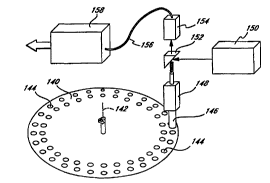
Fig. 14 shows a perspective view of an optical memory
25 in accordance with the invention. A planar optical disk
14 0 is rotatable around an axis of rotation 142 . A
plurality of read portals 144 are disposed upon the
surface of the optical disk 140. The optical portals 144
substantially cover the surface of the optical disk 140.
30 In the preferred embodiments, the read portals 144 may be
arranged in substantially circular tracks or in a spiral
configuration as utilized for conventional optical disks
or compact discs. The ~t~ct~ 146 is positioned proxi-
mally to the read portal 144 subject to reading. In the
35 preferred ~mho~;m~nt, the detector 146 is a near field
f iber optic . A positioning unit 148 serves to vary the
spacing between the detector 146 and the surface of the
~VO9~/34890 2 1 9 t 2;~ O P ~
.
17
optical disk 140. A source of read illumination 150,
preferably a laser, is directed through optics to excite
the chromophoric memory units within the read portal 144.
In one Pmho~;- t, a dichroic mirror 152 may be utilized
5 to direct the output of the laser through the detector
146. Emitted read illumination from the read portal 144
may be passed via the detector 146 through the optics,
such as bandpass f ilters, including the dichroic mirror
132 to a read detector 154. In the preferred embodiment,
10 the read detector 154 may be a single or array of ava-
lanche photodiodes for parallel access. The detector 154
then provides a signal on cable 156 to output electronics
158. In an alternate ~mhorl;m~nt, the optical disk may be
illuminated from below the disk, with the detector remain-
15 ing in the same position above the disk.
Fig. 15 shows a schematic view of the write device.The optical disk media 140 i8 adapted to rotate around its
axis of rotation 142. The optical disk media 140 ,-~n~A;nR
various CI1L~ ,~h~ric memory units in which the ~auencher is
20 active in its initial state. During the course of the
writing, the quencher may be inactivated. Multiple
sources of ill-lm; nA~ n 160 are arranged to provide write
illumination through alignment optics 162, preferably
alignment optics, to a z positioner 164 and near field
25 fiberoptic 166. In this way, any of the various sources
of write ill~m;nAti~n 160 may be directed to the
chromophoric memory units disposed on the optical media
140. A write beam controller 168 is connected to the
sources of illumination 160 to selectively activate the
30 sources. As the optical disk media 140 rotates around its
axis of rotation, the illumination from the sources 160 as
controlled by the controller 168 ; l l llm; nAte various read
portals or subportal size write locations. In this way,
writing occurs as described previously (e.g., Fig. 5, Fig.
35 7b) .
The detailed structure, se~uence and chemistry of the
memory will be described below. The discussion is gener-
W095/34890 2 ~ 9 ' 2~ u Y~ C~ 33
18
ally divided to :focus on DNA Design, Synthesis, Deriva-
tion, Attachment and Organization, Activation, Hybridiza-
tion, ChLL. ~hnric Re6ponse and Write-Details.
DES IGN
The sequences of nucleotides in the bac~cbone 92 (Fig.
9) and complementary donor 94 and acceptor 96 sequences
are designed preferably to self-organize by hybridization
into discrete chromophoric units. The conventional
nucleotide units of adenine (A), thymine (T), guanine (G)
and cytosine (C) are arranged in various sequences. The
conventional pairing is used, with adenine pairing with
thymine and guanine pairing with cytosine. The conven-
tional double helix structure is preferably utilized,
wherein the standard radius is approximately 1. 0 nm and
spacing between~base pairs is apprnl~;r-t-~ly 0.34 nm in a
linear direction along the chain. Such DNA is desirable
f or use in the instant invention in part because of the
precise geometric and distance reguirements of Forster
energy transfer photonics processes. Further, these
sequences are designed for hybridization efficiency and
specificity such that they can self-organize reproducibly
into predicted arrangements of chromophore units. Addi-
tionally, the structures are preferably optimized for
energy transfer efficiency. Finally, it is a desired
aspect of the nucleotide sequences that they are attach-
able to the solid support, preferably the substrate 10.
These DNA sequences range from approximately 20 to
1000 nucleotides in length (i.e., base units adenine,
cytosine, thymine, and guanine) . The shorter DNA polymer
sequences are generally referred to as Oligonucleotides or
oligomers, and a DNA polymer 20 nucleotides in length
would be designated a 20-mer. The actual molecular shape
and size of a 20-mer would approximate a linear rod
structure about 6 . 8 nanometers tnm) long and 1 nm in
diameter (2 nm for double-stranded DNA). Each additional
base unit would add 0 . 34 nm to the linear dimension . A
wo9S/34890 2tq~2~ r~ '0l$5~
19
1000-mer would have a length of approximately 340 nm.
Thus, we will be working with systems that are in the
nanometer regime, ref lecting a high degree of control and
specificity. And, 20-mers to 1000-mers are easily synthe-
sized with available automated instruments and other DNA
technologies .
Sequences are preferably designed for the highe8t
hybridization efficiency and specificity 80 that they will
self-organize reproducibly into the planned molecular
connections and arrangements. This precision is important
because electronic transfer and photonic transfer
~Forster) processes are highly dependent on ~~~;ntislnln~
control over distances between the photonic transfer
groups or the charge transfer groups. Previous work in
1~ solution phase has shown DNA polymers can achieve this
end. It is these mechanism and their associated geometric
requirements that make synthetic DNA the optimal material
for impl~m~nting a man-made system.
Consistent with the above stated design criteria for
DNA structures useful with this invention, various useful
and robust sets of building blocks have been formed for
these photonic systems. The ~ollowing DNA sequences have
been designed for covalent attE~ ' t to metallized or
silicon dioxide ~eatures on silicon surfaces.
Multiple DNA polymer attA~ t sequences have been
synthesized with 3 ' terminal ribonucleosides . These were
designed for covalent attZ~` t to solid supports and the
organization of chromophore labelled polymer sequences.
Twelve (12) amine or aldehyde funct;~n~ ed sequences
were synthesized for reaction with chromophore groups.
From those 12 DNA sequences, 26 DNA-chromophore deriva-
tives were made consisting of 8 distinct colors,
quencher and 1 W sensitive caged chromophore. Table l
shows the current DNA-chromophore conjugates currently
available.
WO 9S/34890 ~ 5~
2fl ~1240
TABLE 1: DNA-Ch.u.,.ùpi-o.~ Conjugates
Ch,u",u~,l,v,c Ex/Em(nm) DNA-Chromophore Conjugate
Fluorescein: 494/519 DO-1F, DO-2F, DO-3F, DOA, DOB,
DOC, DOD, DOE, ET-10-F, ET~ F, T2-
Rhodamine T: 544l570 T2-RT
5 Rhodamine X: 570l596 T2-RX
Bodipy 1: 558l568 ET-14
Bodipy 2: 530l550 T2
Lucifer Yellow: 428l533 ET-10-LY, ET-1 1-LY
Texas Red: 589l615 ET-10-TR, ET-11-TR, ET-12R-TR, ET-14-
TR, ET-21A-TR, T2-TR
10 Napthofluorescein: 600l672 T2-NF
Caged Carboxy- 494l519' ET-13-CF
f luorescein
Malachite Green: 6271none ET-11-MG
'Fluorescent when uncaged by exposure to UV light < 365 nm.
Fig. 16 shows a graph of the inten8ity as a function
of wavele~gth for the 8ix polymer ser~uences.
The spectra for the six curves are listed below in
Table 2.
Peak DNA-CI ,u" .,~ Excitation rnm) Emission (nm)
1 T2 - Fluorescein 494 519
2T2 - Bodipy 2 530 550
3T2 - Rhodamine T 544 570
4T2 - Rhodamine X 570 596
5T2 - Texas Red 589 615
6 T2 - CN Fluorescein 600 672
Fig. 17 shows an .on71~nr-~-1 DNA polymer map. this map
indicates the sequences of all the various DNA chromophore
units relative to the attachment sequences The * por~i-
W0 95/34890 2 1 9 1 2 4 0 r~ 5
.
21
tions indicate the nucleotide sequence which is similar to
the sequences at the center of the diagram.
In addition to the sequences presented in Figure 14,
additional sequences have been designed which allow
5 repetitive chromophoric DNA units to be construced. These
include the att~ - t sequences ATT-1-6; the template
sequences TEM-1-6; and the cl~ h~ric sequences PET-1-C.
The attachment sequences (ATT) are li8ted below (5' and 3'
refer to directionality of the DNA sequence):
ATT-1 5'-GGCTAGCCGAT~G(ilC~ 'AGGTCAAGTCAAT-rA-3'
ATT - 2 5 ' - CGCACTA~ iAGTGTTCAGAGGCTATCAG- 3 '
ATT-3 5 ' -r~r7~r7~rTcATGAGcAGGGGcTAGccGATcGGG-rA-3 ~
ATT-4 5 ' -GACTTGACCTr~r~rrrr~TCGGCTAGCCCCTGCT-3 '
ATT - 5 5 ' -ATGTCTGACTGCAGCTCGr ~ rr.~r.~r7~ rTCATGAGC - rA- 3 '
ATT-~ 5'-GCTAGCCCCTGCTCATGA~l~ L~ ~CGAGCTGC-3'
The following specific DNA se~auences have been
designed to form templates, or to be useful as repeating
structures for spanning di8tances greater than substan-
tially 100 n~n~ . -t~r8. The template sequences (TEM) are
listed below:
TEM- 1 5 ' -ATTGACTTGACCTr-Ar~r~rrrr~TCGGCTAGCC-
- CcAAGcTTGcATGccTGcAGGTcGAcTcTAGAG -
-GA~ e~iG~lACCGAGCTCGAATTC-3 '
TEM - 2 5 ' - GA~TTCGAGCTCGGT - GAATTCGAGCTCGGTACC -
2 5 - CGGGGATCCTCTAGAGTCGACCTGCAGGCATGC -
-AAGCTTGGCCCAAGCTTGGCTGCAGGT-3 '
TEM- 3 5 ' -ACCTGCAGCCAAGCTTGG- CATGATTACGAATTC-
- rrr.Gr.r7~TcCGTCGACCTGCAGCCAAGCTTGGC-
-AcTAGccTcTGAAcAcTrl~rr~Arr~TA-3 ~
TEM-4 5'-TATGCTTCCGGCTCGTA'l-iLl~l~l~,~AATTGTGAGCGGATA-3'
- TEM - 5 5 ' - GTCATAG~: L~ l l l C8~ i L~ l ~AAATTGTTATCCGCTCACAAT - 3 '
TEM- 6 5 ' -ACGTTGT~ rr~rr-r,CCAGTGCCAAGCTTGGCTGCAGAG- 3
Specific DNA sequences have been designed for
functinr~ tion with various photonic transfer
~chromophore or fluorophore) groups and electronic trans-
fer (charge transfer) groups. The photonic/electronic
transfer sequences (PET) are listed below:
_ _ . _ . .... ... . .. .. .. . . . . .. . . . _ _ . _ . _ . .. . . _ _
Wo 95l34890 r~ Sg~
2191240
22
PET -1 5 ' - CCGGGGATCCTCTAGAGTCGA- 3 '
PET - 2 5 ' - CCTGC~GGCATGCAAGCTTGG- 3 '
PET-3 5 ' -GCCAAGCTTGCaTGCCTGCAGGTCGACTCT-3 '
PET-4 5'-AGAGGA`l'~ ,LACCGAGCTCGAATTC-3'
5 PET-5 5'-AGTGCCAAGCTTGGCTGCAGGTCG-3'
PET-6 5~-AcGGATcrcr~ TTcGTAATcATG-3
:i Y ~l L 'l ~ S
The synthesis of short DNA polymer sequences of from
approximately lO to approximately lO0 monomers is a
10 straight forward task for those of ordinary skill in the
art. Automated DNA polymer synthesizers, 6uch as tho3e
from Applied Biosy3tem3 (Foster City, California) automat-
ically 3ynthe3ize u3ing conventional pho3phoramidite
chemi3try. In operation, the nucleo3ide at the 3~-
15 terminus i3 attached to a controlled pore gla33 support by
means of a linker arm. The 5 ' -terminus is blocked with a
th~ytrityl ~DMT) group. First, the support bound
nucleo3ide i9 deprotected to provide a free 5 ' -hydroxyl
group for the att~ of the next nucleotïde. The
20 second nucleotide i8 deblocked and activated at the 3 ' -
hydroxyl with tetrazole to form a highly reactive interme-
diate . The 5 '--terminus is blocked with DMT to prevent
self polymerization. Next, a capping step renders any
chains which do not undergo addition inert to further
25 additions . The ; nt.ornllrleotide linkage is then oxidized
from the phosphite to the more stable phosphate. After
oxidation, the DMT is removed from the growing DNA chain
and the cycle is repeated until chain elongation is
complete. Finally, the fully assembled oligonucleotide is
30 cleaved from the CPG support, deprotected and purified by
polyacrylamide gel electrophoresis (PAGE) or high pressure
liquid chromotography (HP~C) to remove failure sequences.
The att~h~^nt sequences contain 3'-terminal ribonu-
cleoside and are synthesized by initiating synthesis from
35 a ribonucleoside-CPG support. Certain homopolymer attach-
ment sequences are synthesized by enzymatic reaction, and
WO 95/34890 r~ Jb _~
21 ~124~
23
may be purchased f rom commerical sources such as Sigma
Chemicals (St. Louis, MO). Other sequences may contain
amine functionalities and serve as substrates for the
attachment of C~ h~re molecules, including the donor,
acceptor and/or quencher molecules. These polymers have
a 5'-term.inal amine and ;nt~rn~l primary amine groups.
The 5~-terminal amine functionalities are allt~ tically
incorporated by means of the ABI amino link to reagent.
Internal 1 ~h,~1 l; ng of the oligonucleotide is done by
several methods. In the case of fluorescein the chromoph-
ore is automatically incorporated into the polymer at any
position through use of a fluorescein phosphormidite. For
labelling with other chromophores, an amine terminated
linker arm nucleoside phosphormidite is automatically
incorporated into the polymer at any thymine base posi-
t ion .
DERIVITIZATION
Derivit; 7~ti~n is performed in the preferred embodi-
ment as f ollows:
The amine functionalized synthetic DNA polymers are
labelled with chromophore groups and are used in the
energy transfer, qn~nrh;n~ and a write m~h~n;F~ Many
chromophore groups are commerically available in reactive
forms which allow straight forward coupling chemistry to
amine groups. The different chromophores are generally
available in at least one of the reactive forms listed
below:
1. Isothiocyanates (R-N=C=S) which form thioureas
(R=NH- [C=S] -NH-R' ) upon reaction with amines.
Fluorescein, tetramethylrht~m; n~ and rhodamine
- X DNA conjugates are formed by this chemistry.
2. S-]cc;n;m;dyl esters (R-CO2-X) which form
carboxamides R- [C=O] -NH-R' ) upon reaction with
amines . Bodipy dyes, napthof luorescein and
caged carboxyfluorescein conjugates are formed
by this chemistry.
_ .. _ . . _ . ... ... ... . . . ..... .. . .. _ _ _ _ _
Wo 9s/34890 P~ ~5~
2~91240
24
3. Sulfonyl chlorides ~R-SO2Cl) which form stable
sulfonamides (R- [S02] -NX-R' ) upon reaction with
amines. Texas Red conjugates are formed by this
chemi stry .
5 The typical labeling conditions are as follows:
1. Dissolve the amine rnnt~;n;ng oligo in 0.25M
sodium bicarbonate, pX 9.0-9.1 to a final con-
centration of 1 O .D . /units (~5 mM for a 20 mer) .
Substitute 60dium bicarbonate, pH 8 . 3 (uncor-
rected for r~rtirnA with s~rr;n;m;dyl esters.
2. Dissolve the amine reactive r rhrre deriva-
tive in anhydrous dimethylformamide (DMF) to a
final concentration of -lOOmM.
3. Combine 10 ul of DNA and 20 ul chromophore,
chr, , hnre/DNA and incubate at room temperature
f or 1-2 hours .
4. Add 5 ul rnnr~ntrated ammonia to r~uench
unreacted material.
5. ~?urify the material by pa5sing through a G-25
Sephadex column (0.9 x 10 cm) equilibrated in 5
mM sodium acetate, pH 7 . 0
6. Collect fractions and measure ~h5nrb~n~e on
spectrophometer from 230-650 nm. DNA absorbs at
260 nm and the C~lr, ~h~re absorbs at its
excitation maximum.
7. Pool conjugate fractions. Reaction usually go
to ~ 5C96 completion.
8. Analyze 0.1 O.D. product by 20~ polyacrylamide
gel el~ctrophoresis.
9. I.yophilize sample to dryness and re-suspend at
1 O . D . /ul in 5mM sodium acetate .
lO. Load sample onto a preparative 20~ PAGE and let
xylene cyanol tracking dye run ~lO cm into the
gel .
ll. By W backshadowing, cut out gel slice
~nntA~ nr both W absorbing and fluorescent
material .
Wogs/34890 2 1 9 ~ 24 0
12. Crush the gel slice rnnt~;n;nr~ product with a
mortar and pestle and elute product overnight in
lXSSC buffer (0.15M sodium chloride, 0.015M
sodium citrate, pH 7 . 0 ~ .
13. Load the elute onto a pre-equilibrated C1B Sep
Pak (Millipore, Milford, MA) reverse phase
column to remove rnnt~m; nAting polyacrylamide .
14. Wash the column with 20 mls water.
15. Elute the product with 2 mls of 505O acetoni-
trile.
16. Analyze the elute spectrophometrically and then
lyophilize to dryness.
17 . Resuspend f inal product to 1 O . D . /ul in 5 mM
sodium acetate, pH 7 . 0 . Typical yields of pure
final product are approximately 505O of the
starting amount.
ATT ~ T _ 0~ ~ ~ NT 7 ~ TION
Fig. 18 shows the steps associated with the preferred
att~rl t chemistry for ~ff;~inr the cl~ hnriC memory
units 16 to the substrate 10. (See Fig. 1). The surface
of the substrate 90 is amine functinn~l; 7ed with APS .
These then react with aldahyde terminated DNA to form a
covalent bond .
The chromophoric memory units are ~tt~rht~t~ to the
substrate, either directly or through an intermediary. In
the preferred process, a two step process is utilized.
First, the solid surface is activated with primary amine
groups. Second, the DNA att~t' - t ser~uence is converted
to an intermediate f orm which reacts with amine groups .
- 30 The attachment chemistry is stable and robust and is
successful on a variety of substrates, including glass,
silicon and metal oxides. The support bound DNA retains
all of its hybridization properties relative to hybridiza-
tion ef f iciency and nonspecif ic background . A sur~ace
loading factor of approximately 105 - 106 DNA att~rhm~nt
ser~uences per micron is obtained.
wogs/34890 2 ~ 9 ~ 24~ r~ s ~
26
Substrate surfaces are amine functi~-nAl ize~ by 3-
aminopropyltriethoxysilane (APS , Aldrich Chemical Co .,
Milwaukee, WI) which reacts readily with the oxide and/or
hydroxyl groups on metal and silicon surfaces and provides
5 a primary amine functionality. Next, the attAr~ t
se~uence is converted to a reactive dialdehyde form by the
periodate oxidation methods. The amine and aldehyde
groups react readily to form a stable imine or Schiff's
base. The APS reaction is performed by treating the
10 desired surface for 30 minutes with a 10% (v/v) solution
of APS in toulene at 50C. The surface is then washed 3
times in toulene, 3 time6 in alcohol and then air dried
for 60 minutes at~ 50~C. The resultant surface i5 amine
functionalized and is extremely reactive to aldehyde
15 groups present on the periodate oxidized at
se~uences .
ACTIVATION
DNA activation is A _ , l; qh~d in the preferred
embodiment by the following process. The 3~-terminal
20r;hr~n--rl~otide terminus of the atta~l sequences is
converted to a terminal dialdehyde by the periodate
oxidized method. The periodate oxidation reaction is
per~ormed as 1 0 . ~/ul . 1 volume of O . lM sodium acetate, pH
5.2 and 1 volume of 0.45M sodium periodate (made fresh in
25 water) is added. ` The reaction is stirred and incubated at
room temperature for at least 2 hours protected from
light. The reaction mix is then loaded onto a Sephadex G-
10 column (pasteur pipette, 0.6 X 5.5 cm) which is equili-
brated in O.lM sodium phosphate, pH 7.4. Fractions (200
30 ul) are rA~ t~od and 2 ul ali~rtuots are spoted onto silica
T~C plates. The W absorbing fractions are combined and
contain the activated DNA polymer.
The solid support materials is rinsed with O . lM
sodium phosphate, pH 7.4. Aspirate and add buffer suffi-
35 cient to cover the chips, add the periodate oxidizedattachment sequences, at minimum 1 0 . D . per cm2 of surf ace
Wo 95/34890 r~l~u~
2f 91~40
27
area. Mix well and react 1-2 hours at room temperature.
The carbonyl compounds form covalent adducts with amines
by dehydration to imines or Schif f ' 8 bases . The DNA
substrate are then washed twice with sodium phosphate
buffer, twice with lXSSC, 0.1~ SDS (WB=0.15M sodium
chloride, 0.015M sodium citrate, pEI 7.0 and 0.19~ (w/v)
sodium dodecyl sulfate) and twice with lXSSC (0.15M sodium
chloride, 0.015M sodium citrate, pH 7.0). The derivatized
materials are used immediately or stored dry.
~IYBRIDIZATION
The preferred hybridization process is accomplished
utilizing any techniques satisfactory to meet the func-
tional criteria of the invention. In the preferred
lornho~ / the following hybri~l7A~ion technique is used.
The DNA support substrates are hybridized for 5 minutes
with 100-200 nM complementary polymer sequences ~r~nt~;n;n~
a fluorescent group at 37-50C in 5XSSC, 0.1~ SDS (HB) .
The hybridization temperature is estimated by the DNA
sequence composition and by using the formula, Tc = (2 X
A/T) + (4 X G/C). For example, the hybridization tempera-
ture for ET-lOAI~ would be (2 X 8) + (4 X 10) = 56C. The
actual hybridization temperature is 10C lower (45C) to
maximize the extent of hybridization. The support sub-
strates are washed 3 times in prewarmed WB at temperature,
1 minute each. Finally the support substrates are rinsed
in lXSSC at RT and dried by canned air (i.e., Dust-Off).
The support substrates are mounted on a glass slide and
observed by epifluorescence with a ~Jenna Epifluorescent
microscope fitted with a Hamamatsu intensified CCD (ICCD)
- 3 0 camera imaging system .
A loading factor of approximately 105-106 at~A~ l -n~
sequences/um2 is generally adequate. The loading factor is
variable because the APS chemistry modif ies the oxides or
hydroxyl groups whose concentration is dependent upon
3 5 process ing f actors .
-
WO 95/34890 PCT/US95/~6999
21 91240 ~
28
rTT~ ~OrA~)RIC ~ ~UN:ilS
Chromophoric groups which emit fluore9cence in the
generally 500-800 nanometer range and are reactive with
DNA and the amine lAh~1l;n~ chemistry are listed below:
Fluorescent Donor/Acceptor Derivatives:
Texas Red (Em = 610 nm)
Rh~ ~lAmlnf~ (Em = 580 nm)
Bodipy Dyes (Em = 503, 51~, 550, 568, 570,
588, 594 nm)
Lucifer Yellow (Em = 528 nm)
Fluorescein (Em = 520 nm)
Cascade Blue (Em = 425 nm)
Non-Fluore~cent Donor/Quencher Derivatives:
Dimethyl Am; nf~phQnylazophenyl (DABITC)
Reactive Red
Malachite Green
The various wavelengths output f rom a read portal
must be spectrally resolvable. Ut; 1; 7; n~ current detec-
tion techniques, peak separations of irom approximately 10
20 to 20 nanometers between each color are resolvable.
Various photoactive groups with selective W absorp-
tion characteristics useful for the write -hAn; Qm
include:
p-Methoxybenzyl Ethers ~280 nm
p-Nitrobenzyl Ether8 -280 nm
p-methoxyphenacyl Esters ~300 nm
o-Nitrobenzyl Ethers -320 nm
Pyrenymethyl Esters -340 nm
bis-2-~itrobenzyl Acetals -350 nm
3 0 WRITE DETAILS - - The caging group approach has been
prepared as follo~ws. A cage fluorescein (fluorescein-bis-
dimethoxynitrobenzyl ether) is commerically available as
a succinimidyl ester derivative. An ET-13-caged fluores-
cein (ET-13-CF) coniugate is made. The compound is
35 intrinsically nonfluorescent until exposed to W radiation
at less than 365 nanometers. Upon irrzfl;At;~n, the
W095l34890 2~ ~ ~40 l'~,IIL_ ~ ~5~
compound becomes intensely fluorescent at t~e characteris-
tic fluorscene excitation and emission maxima, 490 and 520
nanometers, respectively. See Fig. 15.
Although the invention has been described with
5 respect to specific preferred embodiments, many variations
and modifications may become apparent to those skilled in
the art. It is therefore the intention that the appended
claims be interpreted as broadly as possible in view of
the prior art to include all such variations and modifica-
l o t ions .
' ! ,". ', j , ., ~, ~, _.