Note: Descriptions are shown in the official language in which they were submitted.
~ W0 95133865 21~1~ 5 8 r~ 27
,
LOW TEMPERATURE PLASMA-ENHANCED FORMATION
OF INTEGRATED CIRCUITS
FIFI n OF THE INVENTION
This invention relste5 ~enerally to plasma c.~l,al)ced
chemical vapor deposition li~ECVD) for applyin~ various film coatin~s
to substrates. and more ~Fe 'y to ~ECVD conducted at a low
effective d~p~ iol7 temperature.
~ACKGROUND OF THE INVENTION
In the formation of i~ dL~d circuits (IC's~, thin films
co, ,i.lg metal elements are often deposited upon the surface of a
substrate, such as a .~.."i~.ol,d-Jctor wafer. Thin films are deposited
to provide conducting and ohmic contacts in the circuits and between
the various deYices of an IC. For examp~e, a desired thin film mi~ht
i7e appiied to the exposed surface of a contact or via hole on a
semiconductor wafer, with the fiim passing through the insulative
layers on the wafer to provide plugs of conductive material for the
purpose of making i,~L~,uurln~L~liun5 across the insuiating ~ayers.
Wo 9~33865 2191 4 S 8 -2- r~l,u~ o 1127 ~
One well known process for de~v;,;li.,g thin metal films
is chemical vapor dt:~G ,;liol~ (CVD) in which a thin film is deposited
using chemical reactions between ,Yàrious deiJo;~ ol~ or reactant
gases at the surface of the su~istrate. In CVD, reactant gases rlre
pumped into proximity with a substrate inside a reaction chamber,
and the gases sl Ihse~ r~ntly react at the substrate surface resulting
in one or more reaction by-products which form a film on the
substrate surface. Any by-products remaining after the d~pv .iLion
are removed from the chamber. While CVD is a useful ~ for
depositing films, many of the ~ iLivnal CVD ~u~,e:.3~s are basically
thermal processes and require temperatures in excess of 1 000C in
order to obtain the necessarY reactions. Such a db~,v ,ilion
temperature is often far too high to be ~L '' "~/ useful in IC
rabl i~,c-Livn due to the effects that high temperatures have on various
other aspects and layers of the electrical devices making up the IC.
Certain aspects of IC cu~-v~rl~ are degraded by
exposure to the high temperatures normally related to Llau!iliulldl
thermal CVD p,v~ssas. For example, at the device leYel of an IC,
there are shallow diffusions of :._., .i.,o-~ductor dopants which form the
junctions of the electrical deYices within the IC. The dopants are
often initially diffused usin~ heat during a diffusion step, and
therefore, the dopants will continue to diffuse when the IC is
subjected to a hish temperature during CVD. Such further diffusion
is u";l~i,dLI~ because it causes the junction of the deYice to shift,
21gl~58
woss/33s6~ 3 P~ O~I27
and thus alters the resulting electrical cll~.a~.lcli;.li~, of the IC.
Therefore, for certain IC devices, exposing the substrate to
u,u~ ,;"g temperatures of greater than 800C is avoided, and the
upper tempersture limit may be as low as 650C for other more
temperatùre sensitive devices.
FUIL~ -IIIU~C~ such temperature ~ liul~s may become
eYen more severe if thermal CVD is pc, rul-l,cd after metal
i"lc" o,,,,cuLion or wiring has been applied to the IC. For example,
many IC's utilize aluminum as an i,,lc,uù,,,,euliun metal. However,
various U~ldC~ildUI~. voids and extrusions occur in aluminum when it
is subjected to high p,uce~ g temperatures. Therefore, once
,..o,~ne, Li"g aluminum has been deposited onto an IC, thr~
maximum temperature to which it can be exposed is duulu,-illlaL~
500C, and the preferred upper temperature limit is 400C.
Therefore, as may be du~lc~ ialc-J, it is desirable during CVD
processes to maintain low deposition temperatures v~l,c,l_~a
possible.
Consequently, the upper temperature limit to which a
substrate must bc exposed precludes the use of some Lla~iliul,~l
thermal CVD ~,u~esses which might uLllcl~rJ;-- be very usefui in
fabricating IC's. Titanium and titanium nitride are used in a variety
of IC _p~' ,s. It is frequently desired to form a titanium silicide
contact layer over a silicon surface. This can be formed using
chemical vapor depu~iLiûn of titanium onto the silicon surface. The
, _ _ _ _ _ _ _ _ _ _ _ . .. . . .
W0 9St33865 2 ~ ~ ~ 4 5 8 ~ c sl27 ~
titanium silicide forms as the titanium is depo~it~l Further, in many
a,," ~ s a titanium nitride barrier layer is required prior to
deposition of certain metal conductors such as aluminum ortungsten.
Titanium nitride can be deposited by chemical vapor d~puaiLi~l,. The
byproducts of the chemical vapor de~osiLi~n -- in particular, hydroqen
chloride -- act to etch the titanium contact layer. Therefore, the
titanium must be nitrided prior to titanium nitride chemical vapor
i~:uuailiùl~.
Titanium nitride is frequently deposited onto aluminum
as a contact layer. However, when titanium nitride is deposited onto
aluminum, aluminum nitride is formed at the interface which acts as
an insulator and impedes flow of current from one II~t:i " , layer
to another. The titanium nitride is needed as an adhesion layer
performing tungsten via plugs. To avoid this problem, a titanium
layer is required to protect the aluminum and then permit sputter
dep~ailion of the titanium nitride adhesion layer.
To sputter deposit a film, the target is ~ Ll iu~lly biased
and ions from the p~asma are attracted to the target to bombard the
target and dislodge target material particles. The particles then
deposit Lll~",_~lv~ cumulatively as a film upon the substrate.
Titanium may be sputtered, for example, over a silicon substrate after
various contacts or via openings are cut into a level of the substrate.
The substrate might then be heated to about 800C to ailow the
silicon and titanium to alloy and fûrm a layer of titanium silicide
21914S8
- 5 -
(TiSi2~. After the deposilion of the titanium ~ayer, the excess titanium
is etched away from the top surface of the substrate leaYing TiSi2 at
the bottom of each contact or via. A metal i~L~-~onnection is then
deposited direct~y over the TiSi2.
While physical sputtering provides deposition of a
titanium film at a lower temperature, sputtering processes have
various drawbacks. Sputtering normally yields very poor step
coverage. Step coverage is defined as the ratio of film thickness on
the bottom of a contact on a substrate wafer to the film thickness on
the sides of the contact or the top surface of the substrate.
Consequently, to sputter deposit a predetermined amount of titanium
at the bottom of a contact or via, a larger amount of the sputtered
titanium must be deposited on the top surface of the substrate or the
-~0 r~ ~~
sides of the contact. For example, in order to deposit a~200~film at
Go- loo~ L
the bottom of a contact using sputtering, a~600A to 1 OOOA)fi~m layer
may have to be deposited onto the top surface of the substrate or the
sides of the con.act. Since the excess titanium has to be etched
away, sputtering is wasteful and cost~y when depositing layers
Crj"Ld; ~ 5 titanium.
Furthe~more, the step coverage of the contact with
sputtering techniques decreases as the aspect ratio of the contact or
via increases. The aspect ratio of a contact is defined as the ratio of
contact depth to the width of the contact. Therefore, a thicker
sputtered film must be deposited on the top or sides of a contact that
W095133865 219I~58 r~ 27
-6-
is narrow and deep lhigh aspect ratio) in order to obtain a p2rticular
film thickness at the bottom of the contact than would be necesssry
with a shallow and wide contact (low aspect ratio~. In other words,
for smaller device d;."~ iolls in an IC, cci"~ii,y~n~i~lg to h;gh as5pect
ratio contacts and Yias, sputtering is even more ill~rriuiwll and
wasteful. The decreased step coverage during sputter d6s~Jo~ ion
over smaller devices results in an increased amount of titanium that
must be deposited, thus i~ tse5~;llg the amount of titanium applied
and etched away, i"c, tsasing the titanium deposition time, and
increasing the etching time that is necessary to remove excess
titanium. Ac~c~ld;.l51y, as IC device ~e~ esllicss continue to shrinkand
aspect ratios increase, de, usiLion of titanium-co": , ,g layers by
sputtering becomes very costly.
Further, sputter deprii,iliun requires the utilization of a
separate reaction chamber. In ~ where a first film is
deposited by chemica~ vapor depoi,ilion, which is the preferred
methcd, follow2d by sputter dt:~,oi,iliull of a second film, two
different chambers are required. This could then be followed by a
third chamber where, for example, a metal layer would be sputter
depocit~d. It is certainly ~ r~ ,d~l~. to minimize the transport ûf the
substrate from one reaction chamber to another and to conduct as
many reactions as possible in a single chamber.
One approach which has been utilized in CVD rilu~.e~
to ~ower the reaction temperature is to ionize one or more of the
, .5
, _ _ _ _ _ ,, . . _ , . ,,,, _ _
-
reacTant gases. Such a technique is generally referred to as plasma
enhanced chemical vapor deposition ~PECVD) . However PECVD has
not proven ~o be an efficient method for CVD.
GB Patent Application 2192196 describes a process
for thermochemical surface treatment of materials in a
reactive gas plasma. Combination~i of different alien
elements may be provided in the treated surface. The
processes may be followed by deposition of layers on the
treated surfaces using Physical V2pour Deposition PVD or
Chemical Vapour Deposition CVD.
Thin Solid Films, Vol. 230, No. 2, 10/Oa/93.
Lausanne (CH), p . 115-120 ; B . Kulakowska-Pawlak et al :
~ Spectroscopic investigations into plasma used for
nitriding processes of steel and titanium~ describes
treati~g the surfaces of steel or titanium articles by
nitriding using d.c., r.f. or microwave discharges. In the
experimental apparatus an electrode of 15 mm was employed
Thin Solid Films, Vol. 139, No.~ 3, 02/06/86,
Lausanne ~CH), p.247-260; M.~. Hilton et al: "Composition,
morphology and mechanical properties of plasma-assisted
chemically vapour-deposited TiN films on M2 tool Steel"
describes the deposition of a titanium nitride coating
using either CVD or PVD. In the experimental apparatus on
electrode spacing of l inch (25.4 mm) is provided.
Summar~f of the Invention
It is an object of the present invention to provide
a method oi chemical vapour deposition of films at low
temperatures, generally less than 500 C. Further, it is
an object of the present invention to provide for the
chemical vapour deposition of different films in the same
apparatus. These films would include titanium, tungsten
and/or titanium nitride. Further, it is an object of the
present invention to provide for a method of depositing
these films onto a variety of substrates such as silicon,
aluminurn and tungsten while, at the same time, avoiding
many of the problems typically associated with multiple-
layer deposition such as creation of shorts and/or
21gl458
-7a-
production of undesirable high-resistance films.
A method of depositing a substrate in accordance
with one aspect of the invention comprises forming a
titanium layer on a surface of the substrate by creating a
first plasma of a gas mixture, the gas mixture comprising
titanium tetrahalide and hydrogen wherein the plasma is
creased within about 25 mm of the surface, and nitriding
the titanium layer by forming a second plasma from a gas
selected from the group consisting of ammonia and nitrogen
with 25 mm of the titanium layer, thereby forming a layer
of titanium nitride.
A method of depositing a substrate in accordance
with another aspect of the invention comprises subjecting
a titanium surface to a first plasma wherein the p~asma is
created from a gas selected from the group consisting of
ammonia and nitrogen and wherein the plasma is created
within 25 crn of the titanium surface, and forming a second
plasma from a gas mixture within 25 mm of the surface
wherein the gas mixture comprises titanium tetrahalide and
a gas selected f:rom the group consisting of ammonia and
nitrogen .
The objects and advantages of the present invention are
provided by plasma-enhanced chemical vapor deposition of films onto
substrates wherein the plasma is created in close proximity to the
substrate surface. ~y creating the plasma within about 10
..e"Li",~L~:, of the surface of the substrate, the plasma acts to very
efficiently coat the substrate surface with the desired thin film.
More particularly, employing a showerhead RF electrode
to create the plasma within 25 mm of the substrate surface permits
an even plasma at a relatively low temperature permitting a wide
2191~8
- 8 -
variety of different combinations of films to be deposited upon a
substrate. Further, incorporating a plasma-enhanced ammonia anneal
provides further flexibility in depositing a variety of different films.
This wiil permit PECVD deposition of titanium onto a silicon surface
to form titanium silicide which can be annealed with an ammonia
plasma. This can be followed by PECVD of a titanium nitride layer,
all in the same reactor.
Further, one can use the PECVD method to deposit
titanium over an aluminum substrate fol~owed by nitridi~ation with an
ammonia plasma anneai. This can thus be coated with titanium
nitride using the PECVD method of the present invention.
As can be seen, this provides a method to provide
multiple coatings on a substrate in one reaction chamber.
The objects and advantages of the present invention wiil
be further appreciated in light of the following detailed descriptions
and drawings in which:
Brief Descri~tion of the Drawincrs
The Figure is a side view in partial cross-sec~ion
of a deposition chamber for use in the present invention,
the Disclosure of which is incorporated herein by
ref ererLce .
Detailed Descri~tion of the Invention
The Figure shows one embodiment of a CVD reactor
for use in the present invention. A similar structure is
disc1Osed in pending U. S . Patent Application Serial No .
08/166,745. Modification of this apparatus is disc1Osed in
a U.S. Patent Application entitled ~Method and Apparatus
for Efficient Use of Reactant Gases and p1asmas ~or
depositing CVD and PECVD Fi1m" listing Joseph E~illman,
~obert Foster and Rikhit Arora as inventors, filed on even
date herewith.
2191~8
g
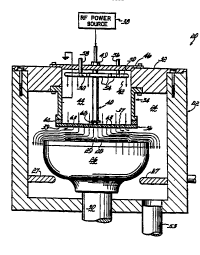
- Reactor 20 includes a
deposition chamber housing 22 which defines a reaction or deposition
space 24. Reactor 20, and specifically reaction space 24 within
housing 22, may be selectively eYacuated to Yarious different internal
GG ~ 3~ ~I~Z
pressures, for example, froml(O.S to 10 Torr,) The susceptor 26 is
coupled to a variable speed motor (not shown~ by shaft 30 such that
the susceptor 26 and substrate 28 may be rotated at various speeds
such as between 0 and 2,000 rpm. Suscepto~ 26 is also heated by
a heating element (not shownl coupled to the susceptor 26 in order
that susceptor 26 may heat substrate 28, such as between 200 and
~OOC.
Extending downwardly from a top wall 32 of housing 22 is a
cylinder assembly 34 which is attached to a gas-dispersing
showerhead 36. Showerhead 36 is suspended above substrate 28
by assembly 34. The cylinder assembly 34, in combination with an
opening 42 formed in the top housing wall 32, forms a generally
vertical flow passage 44 which extends between a housing cover 46
and showerhead 36. Showerhead 36 is coupled to an RF power
2I~ ~5~
-, o-
source 38 by an appropriate RF feedline assembly 40 which extends
through cover 46. A sealing structure 49 seais the opening around
feedline assembly 40. Feedline 40 can include a heat pipe (not
shown) to dissipate unwanted heat.
Plasma and reactant gases are introduced into flow
passage 44 by c,~nc~"L~ ic gas rings 50, 52. The concentric rings 50,
52 include a number of holes 54 which evenly dispense the gases
around the flow passage 44. Ring 50 is connected to a ~as supply
through line 56, while ring 52 is connected to a supply by line 58.
An insulator ring 62 separates cylinder 34 and
showerhead 36 for reasons flic&~c~d hereinbelow. If cylinder 34 is
quartz, insulator ring 62 is not needed. In one ernbodiment of the
reactor 20, cylinder 34 is 1r,~ ic&11y grounded by ground line 61.
The insulator ring 62 preferably has an outer diameter
approximately the same as the outer diameter of showerhead 36.
Insulator ring 62 ensures complete separation of cylinder 34 and
showerhead 36. The insulator ring is preferably made of quartz
material app,u~i"~a~ (O.75 inches)thick.
Showerhead 36 is generally circular and inciudes
6~
di~pe, ~io" holes,6~generally throughout its entire area. The diameter
of the showerhead 36 will depend upon the size of the wafers with
which it is used. The showerhead 36 contains generally from 200 to
G3,200 holes~and preferably from 300 to 600 holes for dispersing
~3 -
the sases. Preferably, the showerhead dispersion holes,6~are sized
2191458
, 1
~ 3to prevent creation of a plasma in holesJ~. Holes approximately 0.1-
1 mm are suitable for this purpose. A suitable showerhead is one
which is 0.64 cm thick with 600 0.8 mm holes with a diameter of
17.3 cm
Showerhead 36 is bolted or screwed to the quartz ring 62.
The showerhead 36 includes a stem 68. Stem 68 is formed integrally
with the showerhead 36 and form part of the RF line assembly 40
which connects to showerhead 36. The sl,o~r_.l,ead, 36, inc~ùding
stem 68, is formed of an electrically conductive materiai preferably
Nickel-200. As may be appreciated other conductiYe materials may
also be appropriate. As shown, the showerhead 36 is totally
insulated from cylinder 34.
CVD reactant gases are introduced into the top of flow passage
44 by concentric gas rings 50, 52. The gases fiow downwardly
through f~ow passage 44 and a velocity profile develops along the
length of the flow passage. That is, the gas flow will develop
different velocities as measured across the width of flow passage 44.
Generally, the velocity of the gas flow at the top of the flow passage
near rings 50, 52 is generally equal ho.i~u,,~ 'y across flow passage
44. However, when the gas flow reaches the top surface 37 of
~I~u~lJ~ e~d 36, the velocity of the gas flow is greater in the center
of the flow passage 44 p~u~d~al~ stem 68 than it is at the sides of
the flow passage 44 near the walls of cylinder 60. At the bottom of
flow passage 44 generally above showerhead 36, the veloci~y~ptofile
2191~8
WO 9!j/33865 ~ 1127
--1 2-
of the ~as flow has reached a steady state. When the reactsnt ~ases
pass through the openings 63 of the showerhead 36, the velocity
profile across the bottom surface 39 of the showerhead has f~attened
out such that the flow velocity ~lo~dllldl~ the center of ~hu.:~ .l,aad
36 is generally equal to the flow velocity at the pe~ iuh~cl edge of the
~i)û rn . I ,ead .
The reduced spacing between showerhead 36 and
rotatins substrate 28 produced by the present invention yields
uniform gas flow over the top surface 29 of substrate 28 and a very
thin boundary layer.
The 51 ,û ~_rl ,~ad 36 is biased with RF energy to function
as an RF electrode for PECVD le- l"~ es The close spacing of the
RF electrode and the resulting co~c~"L,alt:d plasma is very useful for
low temperature PECVD, and particularly for low temperature PECVD
of titanium-containing films.
The RF power source, through RF feedline assembly 40 biases
the ~I~u. .I,aad 36 so that the ~I,u~J_.l,~;ad functions as an RF
electrode. The grûunded susceptor 26 forms another parallel
electrode. An RF field is created p, ~r~, di,ly between showerhead 36
and susceptor 26. 11~ . Idr~l in the r, ~ " ~, sl~o~ ad 36 will
be referred to as ~I,u..~ adlelectrode 36 when referring to a biased
sl,o~_.l,ead 36 in acc~l ia.~ce with the principles of the present
invention. The RF field created by the biased s~lo~ ad/electrode
36 excites the plasma gases which are di~,u~ns~d through holes 63
, _ _ _ .. ... .. _
WO 95/33865 2 1 9 1 4 ~ 8 ~ C 1127
-1 3-
so that a plasma is created i~ edialely below showerhead/r;:s~ ~u~r
36. It is ~l~r~ld~ki that the plasma is created below the
al 1O ~ , I ,aad/elecUode 36 and not within the flow space ~4 above the
a~,oJ~ ,aad/electrode. As ~ ned above, the ~ la;ùn holes 63
are p~ t,dbly d;",a"siùned so that the plasma is confined belowthe
sl,o~L.l,aad/electrode 36. F~llll~llll~l~, other steps are taken to
ensure that the plasma is concer,l,d~ed below the
sl ,u . . _. I ,aad/electrode 36. For ex2mple, insulator sleeves are utilized
within the RF feedline assembly 40 to insulate the RF line from the
metal of cylinder 34 and housing 22. Addiliol 'Iy, quârtz insulator
ring 62 separates the ~ ead/~lL~l uue 36 from cylinder 34 and
further ensures ge,)e,d~i~n of the plasma below the bottom throush
surface 39 of the ~ d~ _Llude 36. The rotation of
susceptor 26 ensures a uniform flow of plasma gas to the plasma for
a uniform depl,:,iLiun.
The reactant gases, such as TiC14 are introduced through rin~s
50 and 52. The gas flow from rings 50 and 52 deYelops within the
length of the flow space 44 as the gas travels to the
,I,u..L.l,eacl/electrode 36. The gas particles of the reactant gas sre
excited by the RF field g~r,~:,dl~d by sl~u~.l,aad/electrode 36 snd
susceptor 26. Therefore, a gas mixture of excited reactant gas
particles and radicals and ions of the plasma gases are co~ce"lld~
above substrate 28 and close to the substrate. In acuuldaln~e with
the principies of the present invention, the cylinder 2ssembly 34 is
... _ ....... .... _ ... ... _ ... _ _ .. .... ..... _ _ _ _ _ _
WO9S/33865 2t9~t~
-~4
el~siol~e~ such that the spacin9 between al lo~ laad~ udr~ 36
and substrate 28 is ularGIably under 25 mm, and more ~IGra~
approximate~y2olll;;;;~llaLala~ As",G"Li~l~edabove,thepressuredrop
across the ~I,o~.~.l,Gad/electrode 36 flattens out the velocity profile
of the plasma and reactant gases as they pass through the Ji;walaiu~
holes 63. This produces a generally equal velocity profile across the
gas mixture above substrate 28 and promotes a uniform de~,u .ilion
of a film on substrate surface 29.
The frequency range of the al 10 ./ U. 1 ~Ga.l/electrode 36 csn
be between. for example, 450 KHz and 13.56 MHz. However, the
invention does not seem to be particularly frequency sensitive. The
unique use of the sl-o~.~ I,Gad/electrode 36 in close proximity to
substrate 28 produces a COrll~G.lll-lLGd plasma with a large density of
useful Qas radicals and ions plU~ G thG substrate surface 29. With
the RF showerhead/electrode configuration of the present invention,
it has been discovered that there does not seem to be a nolil,~a~lu
âllllall~,GlllellL gained in rotating the susceptor 26 faster tha~
app~u~illlcL~ly 100 rpm, although rotation rates of up to 2,000 rpm
or faster are possible. It was also found, however, that a rotation
rate of 0 rpm, although not drastically affecting the dep~ailiun rste,
lowers the uniformity of the reactant and plasma gas flow and the
subsequent d~yG ,;liun.
Since the sho.~. I~Gadlelectrode 36 of the present invention
generates a plasma cul .;. ,9 radicals and ions for a plasma-
_ _ _
21~I~58
-15-
enhanced CVD, the showerhead spacing and deposition pdldlllt:L~
must be chosen to achieve a useful mixture of radicals and ions at the
substrate surface 29. While some ion bo",bd"i-lle"~ of the substrate
28 is beneficial because it supplies additional energy to the growing
film layer on the surface 29, too much ion bombardment of substrate
28 may damage the integrated circuit devicss on the substrate.
Furthermore, a high density of ions leads to poor film conform2~ity as
ions have a tendency to stick to contact and via surfaces.
~ 4
Finally, waste gases are removed from reaction space,l4
through port 53. Baffling 27 may be provided to even the gas flow
around the susceptor 29.
This reaction 20 is useful in plasma-enhanced chemical
vapor deposition of titanium, tungsten, titanium nitride, titanium
silicide, and is useful for the annealing of a previousiy-deposited
titanium film to form titanium nitride. The underlying invention, in
turn, relies on the ~.u",l,i,~d~ion of these processes.
The underlying substrate can be any typica~ IC subs~rate
including silicon, TEOS (tetra ethyl ortho silicate~, or quartz, as well
as such substrates coated or partially coated with metal conductors,
contacts, insulating layers and the like.
To deposit a titanium film according to the present
invention, titanium tetrahalide such as titanium L~Lld-,llloride is added
with hydrogen and is injected through injector rings 50 and 52. In
this reaction, the flow rate of titanium tetrachloride should'~'e about
2191~
-1 6-
2 to about 100 sccm (generally about 5 sccm) with a significant
molar excess of hydrogen gas. Generaily, the hydrogen gas flow rate
will be 10 to about 300 times that of the flow rate of titanium
tetrachloride. Argon can also be used and the hydrogen gas partially
released accordingly. The gas inlet temperature for these combined
gases is established at about 400 C to about 800 C with the
substrate heated to a temperature of about 375 C to about 850 C.
The pressure of the reaction chamber can vary from 0.1 to about 20
1 3 33 ~ ~
torr, generally~(0.5 to 10 torr,~ At higher pressures a plasma will not
form.
The RF electrode is operated at between about 100
watts up to, as a maximum power, the power at which the devices
are damaged, which would be about 5 kilowatts. However, for
practical purposes, about 250 watts is sufficient. The frequency of
the RF electrode is set at from about 33 MHz down to about 55 KHz,
with about 13.56 MHz being acceptable. This frequency is a
frequency established by the Federal Communication Commission and
therefore most equipment is set up for this frequency. However, it
is certainly not determined for the 0p~ aLiun of the present
reaction.
Thus, the combined gases are iniected into cylinder 34,
pass through RF electrode/showerhead 36. A plasma is created and
the titanium is formed and deposits onto the substrate 28. The
hydrogen reacts with the halide, i.e., chlûride~ to form hydrogen
--1 7--
chloride which is exhausted. The reaction is continued and the
titanium film is deposited until a desired thickness of film is applied.
Depending upon the particular ~ on, this can vary from about
lO~ oao v~
~00 angstroms)to abou2(20,000 angstroms~ solely dependant upon
the desired application.
If tungsten is desired, the reactant gases are a tungsten
halide such as tungsten hexaf~uoride and hydrogen gas. The tungsten
hexafluoride is added through lines 50 and 52 at a flow rate of 2 to
about 100 sccm (preferably about 5 sccm1 with, again a substantial
molar excess of hydrogen gas. Argon is also added, as necessary to
maintain pressure. The susceptor temperature will range from about
375 C to about 850 C.
Again, the RF electrode should be established at about
the same frequency and wattage as that set forth for the deposition
of titanium. A plasma is thus created forward of showerhead/
electrode 36 and tungsten is formed and deposited on rotating
substrate 28. The tungsten film can be deposited to any desired
thickness and the waste gas will be a combination of unreacted
hydrogen and hydrogen fluoride.
For the formation of titanium silicide, a titanium halide
gas, preferably titanium L~LId~ ide, is reacted with silane to form
titanium silicide and hydrogen ch~oride. The reactant gases are
injected through rings 50 and 52 into cylinder 34 and through
showerhead/electrode 36. The electrode at 13.56 MHz will form a
~gl4~
- 1 8-
plasma from the reactant gases. The plasma wiil contact the
substrate 28, thus forming titanium silicide on the surface 29 of
substrate 28. The preferred reaction conditions for this reaction are:
TiCI4 Flow Rate: 2 to 100 sccm
Silane Flow Rate: 2 to 100 sccm
Inert Gas As needed to maintain pressure
Temperature: 375 C to 850 C
Rotation Rate: 100
Pressure: (0.5 to 20 torr)
~ G~ 6C~ ~Z
An inert gas such as argon or helium is introduced, as necessary to
maintain pressure.
Finally, titanium nitride can be deposited by reacting
titanium tetrachloride or other titanium halide with a source of
nitrogen such as ammonia gas or a co~ ldLiol1 of nitrogen and
hydrogen to produce titanium nitride and hydrogen chloride as a
byproduct. The flow rate of titanium halide should preferably be from
about 0.5 to about 20 sccm. The flow rate of nitrogen source ~qas
should be from 1 to 200 sccm, with 1 to 5,000 sccm of hydrogen,
argon or helium. In all of these reactions, the electrode power, as
well as the frequency, can operate within the same pdldlllt:Lrl~ for
deposition of Ti and the rotation rate remains about the same.
One final reaction which can be conducted in the
apparatus of the resent invention and used ben~ri-,ially in the present
invention is the ,1il1ir~i~dLion of a previously-deposited titanium film.
In this reaction, where the susceptor is previously coated with a
titanium film, the titanium fiim may require nitridization. This can be
conducted by reacting the surface with an ammonia plasma. The
2191~8
flow rate of the ni~ idi~dLiun gas can be from about 10 sccm to about
5,000 sccm. Preferably, the frequency will be about 480 KHz. The
temperature of the reactlon can vary from about 650a C down to
about 300 C with a preferred temperature being less than 500 C,
referably 400-450 C. The pressure must be suL,dL,,,rj:.uheric in all
t~6~
of these reactions and generally can vary froml,~;OO millitorr)up to
~ 16C,', NlmZ 1333 Nl~?
abouq(20 tûrr) with aboutl~ torr)being preferred. In the ni~ dLion
reaction, the reaction time can vary from 1 minute to about 10
minutes, with about 5 minutes being preferred. These reactions will
be further appreciated in light of the following detailed examples.
Example 1
Utilizing the deposition configuration, a layer of titanium
nitride was deposited upon a substrate wafer at app,u~ ldL~ly a
temperature of 400 C. Specifically, a layer of titanium nitride was
deposited using ammonia gas (NH31 and nitrogen gas (N2) with the
pdldlll~ listed below and the results shown in Table 1.
Deposition F~-ldlllt:Lt:la for Table No. 1:
TiCI4 (sccm) 10
NH3 (sccm) 500
N2 (sccm) 500
RF Power (watts~ 250 @ 450 KHz
Reaction ChamberPressure (Torr) 1 = 133 ~1
Susceptor Rotation Rate (rpm) 100
Substrate Temp. (C) 400
2191458
-20-
5 TABLE NO. 1
I ~ , O~
RESULTS AND ADDITIONAL DEPOSITION PARAMETERS
Wafer TiN laver Depcsition Layer Resistivity Dep~siticn Susceptar
Nc.thickness IA~ Rate (A/min~ ~ -cm~ Time ~sec~ Temp (CI
800400 1 5 1 9 1 20 41 4
2 698 348 1 1 94 1 20 471
3 608 304 970 1 20 457
4 545 272 940 1 20 461
5 723 241 1021 180 462
6 910 303 1284 180 475
Wafers 1-3 were si~icon, while wafers 4-6 were thermal
oxlde wafers having a thin layer of silicon dioxide on the surface.
This was done to ensure that the procss of the present invention
may be utilized in a broad ranse of CVD r, F' Lions for both silicon
wafers and oxide wafers. Each of the substrate wafers of Table 1
were also given an RF plasma ammonia ~NH3) anneal in the reactor 40
at 250 Watts for applu~ dlely 120 seconds with a gas flow rate of
CGG 6 I~I¦~Z
5,000 sccm of NH3 at a pressure fll5 Torr~ The rotation rate of the
susceptor during the anneal was a,up~ùxillldlt:ly 100 rpm. The NH3
RF plasma improves the film quality of the deposited TiN film as
discussed further hereinbelow.
The RF plasma electrode/showerhead configuration, in
acco,dal~ with the principles of the present invention, may be
utilized to deposit a titanium nl,tnde (TiN) layer on a substrate utilizins
both nitrogen gas ~N2~ and hydrorden gas (H2) instead of ammorlia gas
(NH3). The various film results and deposition parameters for the H2
... _ _ _ _ . _ _ . .. _ _ _ . . . . _ _ _ _ _ .. ..
21914~8
-21 -
and N2 low temperature deposition of TiN are giYen below in Table
Nos. 2, 3, 4 and 5, at increasing deposition temperatures for
increasing table numbers.
DeDosition Pdlc~ for Ta~le No. 2
TiCI4 ~sccm) 10
H2 (sccml 500
N2 (sccm) 500
RF Power (wattsl 250 @ 450 KHz
Reaction Chamber Pressure (Torr~ 1 - 133 I~l l m~
Susceptor Rotation Rate (rpm) 100
Substrate Temp. (C~ 400
Deposition Time 180 (seconds)
TABLE NO. 2
RESULTS AND ADDITIONAL DEPOSITION PARAMETERS
Wafer TiN layer Depcsition Layer Resistivity Susceptor
Na.thickness (A) Rate (AJmin~ ~-cm~ Temp (CC)
825275 1,530 470
21,023 341 26,864 480
31 ,221 407 4,1 1 8 488
41,262 421 3,108 470
51,227 409 855 470
61,2~4 408 4,478 460
71, 1 41 380 3,982 460
81,348 449 4,658 460
91,400 487 3,449 460
101,106 389 4,501 460
Wafers 1 and 2 of Table No. 2 were silicon, whi~e
the remaining wafers 3-10 were thermal oxide. Wafers 6-10 received
a 250 Watt RF plasma anneal for 120 seconds at an NH3 gas rate of
2191~8
4~ ~
5,000 sccm, at internal pressure fl(3 torr~(wafer 6 was done at 5
torr), and a susceptor rotation rate of 100 rpm.
Table No. 3 illustrates the results of deposition runs
utilizing a substrate temperature of 450C, but ",a;.,~d;,~ g the same
gas and deposition pa~d~ , as were used in the deposition runs of
Table No. 2. Wafer 1 and 2 were silicon while wafers 3-8 were
thermal oxide. The results are as follows with wafers 6-8 of Table
No. 3 receiving a 120 second RF plasma ammonia annea~ at 5000
6cc G I~II~Z
sccm,L~5 Torr)and a 100 rpm rotation rate with a power level of 2S0
Watts.
TABLE NO. 3
~ _ a . I h r~
RESULTS AND AODITIONAL DEPOSITION PARAMETERS
Wa~er TiN laysr Deposition Laycr Resistivity Suscsptor
No.thickness (A~ Rate (A/min~ cml Temp (~CI
9g6332 640 5 1 8
21,069 336 607 519
31,064 355 666 521
41,488 496 815 524
51,562 521 821 521
61 ,444 481 7,1 21 522
71,381 454 5,812 524
81,306 435 6,363 523
The low temperature TiN deposition was repeated with
the substrate temperature at 500C and the results are tabulated
according to Table No. 4 beiow. Wafer 1 was silicon and wafers 2-7
were thermal oxide.
21gl45~
-23-
TABLE NO. 4
I A - o l ~
RESULTS AND ADDITIONAL DEPOS~TION PARAMETERS
Wafer TiN layer Deposition Layer Retistivity Susceptor
No.thickness (~1 Rate (A/min) (~Q-cm) Temp ~C~
990330 578 579
21,086 362 687 590
3.1,034 345 700 597
41,092 364 786 595
51,004 335 1,892 5g1
61,001 334 1,840 593
71,004 335 1,886 594
Wafers 1-4 in Table No. 4 we~e not annealed, while
wafers 5-7 were annealed using a similar RF plasma NH3 anneal
process and the ~.c,c,,,,~r:, used for the deposition runs r~:r~.~nced
in Table No. 3.
Similarly with a substrate temperature of 600C, the
CVD process of the present invention was used to deposit TiN with
the results shown in Table No. 5 below, with wafers 1 and 2 being
silicon and wafers 3-8 beins thermal oxide.
21gl~58
-2~
TABLE NO. 5
As 0, v~w.
RESULTS AND ADDITIONAL DEPOSITION PARAMETERS
Wafer TiN layer l~eposition Layer Resistivity Susceptor
No.thickness (,41 Rate (Almin~ Q-cm) Ternp (C~
657 21g 3g1 650
2822 274 254 650
3740 247 432 650
4768 263 543 650
5767 256 471 650
6765 255 g4g 650
7773 258 g73 650
8g10 303 2 710 650
Again an RF plasma NH3 anneal was pe,tu""ed on
substrate wafers 6-8 of Table No. 5 similar to the anneal step of
133 r~ l~z 6G6~r ~l~z
tables 3 and 4 except at a pressure Ufl~l Tor~instead fl(5 Torr~
Therefore the deposition of TiN using the low temperature CVD
process of the present invention may be accomplished at various
temperatures lower than the temperatures necessary for L~ddiLiona
thermal CVD.
While titanium nitride may be deposited with the present
invention/ it may also be desirable to deposit simply a layer of pure
titanium. For example, a titanium layer might be deposited upon a
silicon wafer which then reacts with the titanium to form a film of
titanium silicide (TiSi2). To this end the present invention may also
be used to deposit a layer of titanium.
21914~8
-25 -
Table No. 6 below sets forth the results and pdldlllt~
of a deposition run which resulted in a deposited film of
approximately 84% titanium on a thermal oxide wafer at 650C.
This was an excellent result for such low temperature chemical vapor
deposition. The deposition run of Table 6 was pe, ru""ed according
to the following deposition parameters, with the RF
showerhead/electrode configuration of Fig. 2.
DeDosition Pa, dl I Id~ for Table No. 6
TiCI4 (sccm) 10
H2 (sccm) 500
RF Power ~watts) 250 @ 450 KHz
Reaction Chamber Pressure ~Torr) 1 = 1~ ~ ~l ~Z
Susceptor Rotation Rate (rpm) 100
Deposition time (sec) 2700
- Substrate Temperature (C) 650
TABLE NO. 6
l A _ o . ~
RESULTS AND ADDITIONAL DEPOSITION PARAMETERS
Wafer Ti layer Deposition Layer Resistivity Susceptor
No. thickness ~A~ Rate (~/min) ~Q-cml Temp (~CI
1,983 44 g29 651
The substrate wafer of Table No. 6 was not annealed.
Additional Ti-layer deposition runs were made according
to the Table No . 7 p~l dl I l~ldr:~ below with the following results shown
in Table No. 7:
~ g~58
~;
-26-
DeDosition Fald~ la fQr Table No. 7
TiCI4 (sccm~ 10
H2 (sccm) 500
RF Power (watts) 250 @ 450 i<H2
Reaction Chamber Pressure (Torr~ 0.85 - 1~3 ~ l~
Susceptor Rotation Rate (rpmi 100
Deposition time (sec) 120 (wafer 7 for 180 sec)
Substrate Temperature (C) 565
Susceptor Temperature (~C) 650
TABLE NO. 7
I ~ . o~
RESULTS AND ADDITIONAL DEPOSITION PARAMETERS
Wafer Tj lave~thickness (~ Oeposi~on Layer Resistivity
No. Rate ~A~min~ ~Q-cm~
134.8 67.4 2 116.1
2 466.2 233.1 1 767.8
3 209.2 104.6 761.8
4 100.8 50.4
1 94 04 97.0
6 1 54.98 77.5 ---
7 115.92 38.6 1 001.4
8 114.7 57.3 371.6
9 152.5 76.2 321.6
39.06 19.5 ---
11 41.6 20.6 ---
1 Z 50.4 25.2
Since a benefit of chemical vapor deposition of titanium-
containing films is improved step coverage and film co ru ~.. .ly over
the physical deposition techniques several of the film layers
deposited according to the present invention were tested to measure
conformality and step coverage. The layers tested for col1ru lll .l;ly
2~91458
-27-
and step coverage were deposited according to the pd~d~ L~r:. of
Table No. 8 with the results shown in Table No. 8 below. The film
conformality and step coYerage of the film layers deposited according
to the pa~d"~e~ below were very good.
DeDositisn Parameters for Conformalitv and Steo Coveraqe
C)erosition Runs of Table 8
TiCI (sccm) 10
Hz ~sccm) 500
N2 (sccm) 500
RF Power (watts~ 250 @ 450 KHz
Reactor Chamber Pressure ~Torr) 1 , 1 3 3 N I ~ Z
Susceptor Rotation rate (rpm) 100
Substrate Temperature (aC~ 450
Susceptor Temperature (C1 520
TABLE NO. 8
I A . o ~
RESULTS AND ADDlTtONAL DEPOSITION PARAMETEPS
Wafer TiN layer Decositicn Layer Resisti~lity Susceptor
No. thiclcness ~,4) Rate (~/min~ ~-cm) Temp ~C~
586 362 -~ 520
2 2.423 304 ---- 520
None of the wafers used in Table 8 and tested for step
coverage were annealed with an RF plasma of NH3.
As illustrated above a layer of titanium nitride (TiN) may
be deposited in accu, da,1ce with the principles of the ptesent
invention without utiiizing ammonia gas (NH3). Instead, a mixture of
H2 and N2 gases is used. Low temperature dd~siLioll of titanium
nitride usin~ TiCI4, N2 and H2 is desirable because it reduces
- 21~1~5g
-28-
~,o.,Ld~"i"a"~ within the reaction chamber that are formed by the
chemical reactions of TiCI4 and NH3. More spe~,iricd'ly, TiCI4 reacts
with NH3 at temperatures below 1 20C to form a yellow powdery
adduct, and to prevent the adduct from forming it was necessary in
the past to heat the reaction chamber walls to at least 1 50C. Since
it is now possible to deposit a layer of titanium nitride at low
temperatures using TiCI4, N2, and H2 chemistry instead of NH3, it is
no longer necessary to remove a deposited adduct or to heat the
reaction chamber walls, thus greatly reducing the cost of CVD
systems.
According to the deposition pdldllld~dl~ of Table No. 9,
a layer of titanium nitride was depositPd upon several therma~ oxide
substrates using a reaction chamber with unheated walls and a gas
mixture of H2/N2. After the deposition of the films, the reaction
chamber was inspected and there was no evidence of a yellow
adduct found. None of the wafers of Table No. g were annealed with
an RF NH3 anneal.
Paldl11dl~1~ for Adduct Test of Table No. 9
TiCI4 (sccm) 10
N2 (sccm1 500
H2 Isccm) 500
RF Power (watts~ 250 @ 450 KHz
Reaction Chamber Pressure (Torr) 1 ~ 1 33 ~ ~ v~
Susceptor Rotation rate (rpm~ 100
Substrate Temp. (C~ 450
Deposition time (sec) 95
Susceptor Temperature (~C) approximately 520
~gl~5~
-z9-
TABLE NO. 9
I /~ ~ O I h w~
RESULTS AND ADDITIONAL DEPOS~TION PARAMETERS
Wafer TiN layet Deposiion Layer Resistivity S~lsceptor
No.thickness ~A) Rate (A/min~ cm~ Temp (CC~
9458 2,1 64 525
2 132 83 2,118 523
31 27 80 1 ,377 520
4 143 90 660 520
51 43 90 764 520
6 160 101 905 523
71 62 1 02 738 521
81 62 1 02 830 520
9 195 123 689 519
1 0204 1 29 702 523
Further deposition runs were made wherein the plasma
and reactant gas flows were adjusted, as well as the internal
deposition pressure. For example, the depo:,ilion runs shown in
Table 10 utilized a higher flow rate of H and an increased deposition
133 ~ ~-.C- G ~ 2
pressure from~1 Torr to 5 Torr). Further, Atgon was mixed with the
H2 fr some of the deposition runs.
Pal dl I ~ e~ ~ for Table 10
TiCI4 (sccm) 10
H2 (sccm~ 2,000 (wafers 1-4);
1,500 (wafers 5-9
Argon (slm) 0.5 (wafers 5-9)
RF Power (watts) 250 @ 450 KHz
Reaction Chamber Pressure (Torr) 5 , 6C6. 6 r`J
Susceptor Rotation rate (rpm) 100
Substrate Temp. (C) 565
Deposition time (sec) 300 (600 for wafer 9)
Susceptor Temperature ~C) app,u~-i",dl~ly 650
2191458
-30-
TABLE NO. 10
I A = 0~
RESULTS AND ADDITIONAL DEPOSITION PARAMETERS
Wafer Ti layerlhickness Oeposi~ion Rate Laver Resistivi~
No. 1~) (A/min) (~JQ-cm
94 58 2, 1 64
21 32 83 2,21 8
3127 80 1,377
41 43 90 660
51 43 90 764
6160 101 905
71 62 1 02 738
81 62 1 02 830
91 95 1 23 689
In Table 10, the flow of H2 was increased to 2,000
sccm for wafers 1-4 and 1,500 sccm for wafers 5-9. The deposition
GC~:- 6
pressure was increased to~ Torr~ F~r wafers 5-9, a flow of 0.5
standard liters per minute (slm~ of Argon was utilized with the H2 as
a diluent. In Table 10, wafers 1-2 and 5-6 were silicon, while wafers
3-4 and 7-9 were thermal oxide
Table 11 shows additional runs made with the increased
H2 flow and increased deposition pressure.
21914~8
-31 -
DeDosition Parameters for Taole No.11
TiCI4 (sccm) 10
H2 (sccm) 1 ,500
Argon (slm) 0.5
RF Power (watts) 250 @ 450 KH~
Reaction Chamber Pressure (Torr~ 5 ~ CCC~ -G
Susceptor Rotation Rate (rpm) 100
Deposition time (sec~ 300
(wafers 9-12 600 sec~
Substrate Temperature (C) 565
Susceptor Temperature ~C) 650
TABLE NO. 11
I A . o ~
RESULTS AND ADDITIONAL DEPOSITION PARAMETERS
af6r Ti layer thickness Deposition Rate , Layer ResistlvitY
No. (~ /min) ; (~-cm~
67.4 2,116.1
2 233 . 1 1 ,767.8
3209.2 104.6 761.8
4 50.4
51 94.04 97.0 ---
6 77.5 ---
71 5.92 38.6 1,001 .4
8 57.3 371.6
9 76.2 321.6
1039.06 19.5
1 1 41.6 20.6 ---
1 2 50.4 25.2
133 ~o G~6 C~`J lw.
The change in deposition pressure froml(1 Torr to 5 Torr)
produced a more stable and symmetric plasma. Additionally, the
.
increased hydrogen flow with the addition of a small flow of Argon
. . . _ , . , _ _
21~1458
-32-
increased the stability of the plasma flow as well as the plasma
intensity. An ar~on flow of 0-10 slm is p, ~:rl~dbld~ Wafers 1-2 were
silicon, while wafers 3-10 were thermal oxide. Wafers 11 and 12
were borophospho-silicate glass, available from Thin Films, Inc. of
Freemont, California. None of the wafers of either Table 10 or 1l
were annealed with a NH3 plasma anneal.
Table 12 shows additional deposition runs at a susceptor
temperature of 450CC.
DeDosition Pdldllld~ for Table No. 12
TiCI4 tsccm~ 5
H~ (sccm~ 1,500
Aroon (slm) 0.3
RF Power (watts) 250 @ 450 KHz
Reaction Chamber Pressure (Totr) 5 666 . 6 I\ll_.Z
Susceptor Rotation Rate (rpm) 100
Substrate Temperature lCC~ 450
Susceptor Temperature ( cc) 450
TABLE NO. 12
I A, ~
RESULTS AND ADDITIONAL DEPOSITION PARAMETERS
Wafer TN layer Oeposition Rate Laver ResistiYitv
No. thickncss (Al ~A/min~ -cm1
9g0 330 578
21,086 362 687
31,034 345 700
41,092 364 786
51,004 335 1,892
61,001 334 1,840
71,004 335 1,886
~g~
-33-
Wafers 1-4 were silicon, wafer 5 was thermal oxide
while wafers 6 and 7 were an aluminum alloy containing aluminum
silicon and copper. Runs 6 and 7 of Table 12 illustrate the viabiljty
of depositing a titanium-containin~ film on aluminum usin~ the
present invention. The deposition runs of Table 12 utilized a lower
fiow of reactant ~as than the runs of Table 11, i.e., 5 sccm of TiCI4.
The deposition runs of Table 13 were made at further
reduced TiCI4 flow rates. All of the wafers of Table 13 were thermal
oxide. None of the wafers of Table 12 or 13 were annealed with an
NH3 RF anneal.
DeDosition Parameters for Table No. 13
TiCI (sccm) wafers 1-2, 4 sccm;
4 3 4, 3 sccm;
5-6, 2 sccm; and
wafer 7 at I sccm
H2 (sccml 1,500
RF Power (watts~ 250 @ 450 KHz
Reaction Chamber Pressure (Torr) 5 CGc . 61
Susceptor Rotation Rate (rpm) 100
Deposition time (sec) 300
(wafers 1 and 2 at 180 and 240, respectively)
Substrate Temperature (C~ 450
Susceptor Temperature (C~ 450
21914~i~
-34-
TABi_E NO. 13
J 1~ z o ~
RESULTS AND ADDITIONAL DEPOSITION PARAMi--TERS
Wafer n layer Deposition Layer Resistivity Susceptor
No.thickness (,4) ~ate ~A/minl (u~-cmi Temp lC)
990 330 578 579
21,086 362 678 590
31.034 345 700 597
41,092 364 786 595
51,004 335 1,892 591
61,001 334 1,840 593
71,004 335 1,886 594
According to the present invention, multiple layers are
deposited onto the substrate. The procedures previously described
for deposition of individual layers of tungsten, titanium, titanium
nitride, or titanium silicide are empioyed to deposit a first layer onto
the substrate followed by a different second layer. The second layer
would also be deposited according to the procedures previously set
forth. Optimally, additional layers can be deposited. When
advantageous, an ammonia anneal would be used.
An integrated contact l~1dldli~d~ion process can be used
by first depositing titanium onto a silicon surface by PECVD. This wili
form a layer of titanium silicide. After the titanium deposition an
ammonia plasma anneal is pd~u~ ed to provide an upper layer of
nitrided siiicide titanium. Finally, a titanium nitride layer can be
deposited by PECVD, again in the same reaction chamber. Finally,
following the deposition of the titanium nitride, aluminum or tungsten
2191~
WO 9S/33865 r~ '.'C 1127
-35-
metal can be spuKer deposited. This fina~ de~,o,;~i~n, however,
would require a separste chamber using spuKer d~pos;~io"
tecnnology. AnyspuKer~epo~i~ionclldllll~l ~ypicallyemployedcould
be used for the present invention. The method of sputter d,~ siliu,)
is well known to those skilled in the art and, per se, forms no part of
this invention.
The present invention can also be used to form
protective layers for aluminum contacts. When titanium nitride is
deposited onto aluminum 1l ' n, aluminum nitride is formed at
the interface. This is an insuiator and therefore impedes the flow of
current from one Illc:Lclli~,Liul) layer to another. The titanium nitride
layer is needed as an adhesion layer for forming tungsten via plu~s.
To overcome this problem, a titanium layer is deposited onto the
preYiously-deposited aluminum layer using the PECVD process
preYiously described. The titanium layer is then subjected to a p~asma
enhanced ammonia anneal, also as previously rlicc~cc~d Finally, a
thicker layer of titanium nitride can be deposited using the PECVD
process of the present invention. Thus, the d~rqCitpd titanium laver
will protect the aluminum layer, preventing formation of aluminum
nitride due to reaction with titanium nitride. Again, this can all be
done in one reactor where previously two spuKering chambers would
have been required. This thus provides for a single chamber CVD
multi-level " ,~ process .
21914~8
-36-
Furthe-, the present invention can be used to apply a
titanium nitride film over a titanium film. The titanium film can be
deposited over any substrate according to the PECVD method
previously described. The titanium is next subjected to a plasma
ammonia anneal, as previously discussed, to form an adhesion layer
of titanium nitride. Titanium nitride is then deposited by the PECVD
method of the present invention. When depositing a titanium nitride
fiim over a nitrided titanium film, it may be preferable to do this in
two steps. In an initial step, the titanium can be deposited in titanium
tetrachloride depletion, i.e., titanium ~ dcl1loride flow rate of 20
sccm with a flow rate of ammonia of about 500 sccm with 5 liters
10 i~ 6 0 h ~
per minute of nitro~en as a diluent. After a thin layer -- about(100 to
500 angstrom~--of titanium nitride has been dr positPd~ the flow rate
of the titanium tetrachloride can be turned up into the saturation
regime, i.e., about 80 sccm, with the ammonia and nitrogen rates
remainin~q constant. This can be deposited to a desired thickness and
the conformality should be about 100%.
Whlle the present invention has been illustrated by the
description of embodlments thereof, and while the embodlments have
been descrlbed in co~,~idd,cblr detail, the scope of the present
Invention should not be limited to such detail. Additional advantages
and modifications will readily appear to those skilled In the art. For
example, the low temperature CVD technique of the present invention
may be utillzed to deposit other films besides the titanium-uollic;~1;ng
2191~58
-37-
films ~ ed in extensive detail herein. ~urthermore, activated
radicals of gases other than H2 and N2 might also be utilized to lower
the deposition temperature.