Note: Descriptions are shown in the official language in which they were submitted.
- . 2 1 9 1 55 1
DIGITAL CIRCUIT FOR DIFFERENTIAL RECEIVER FOR
DIRECT SEQUENCE SPREAD SPECTRUM SIGNALS
DESCRIPTION
TECHNICAL FIELD
The present invention relates to a digital circuit for a differential
receiver for direct sequence spread spectrum signals.
PRIOR ART
Direct sequence spread spectrum modulation has been used for many years,
particularly in radio communications with satellites and in the military
sector.
In a digital data transmitter using conventional modulation, the data to be
transitted modulate a radio carrier. The modulation used can be phase,
frequency or amplitude modulation or a mixed modulation. For simplification
purposes, reference will only be made to phase modulations, which are at
present the most widely used.
The digital data to be transmitted are bits, which have a period Tb, i.e.
every Tb it is necessary to transmit a new bit. With these bits, it is
possible to form groups of bits, also known as symbols, whose period is
designated T and is a multiple of Tb. These symbols modulate the radio
carrier, e.g. in phase.
This procedure can be illustrated by two examples of phase modulation:
a) modulation known as BPSK (Binary Phase Shift Keying) consisting of
allocating a phase state, e.g. O, to the O bits and a phase state 1r to the 1
bits, in which case, the symbol is the actual bit and T =Tb, the radio
carrier phase state being imposed on every bit;
b) modulation known as QPSK (Quaternary Phase Shift Keying), which consists
of using symbols formed by two successive bits, which can therefore assume
four states (00, 01, 10, 11) and a carrier phase state is allocated to each
of these states and in this case T =2Tb and the phase state of the radio
B 12321.3 RS
21 91 551
~`
-- 2 --
carrier is imposed every two bits.
On the reception side it is necessary to demodulate the signal received.
there are two major demodulation families, namely coherent demodulation and
non-coherent demodulation. The coherent demodulation procedure consists of
forming in the receiver a subassembly having the function of estimating the
mean phase of the carrier, so as to reconstitute a phase reference. This
phase reference is then mixed with the signal received to demodulate the data.
The non-coherent demodulation procedure is based on the observation that it
is sufficient for the phase reference of the symbol taking place to be
compared with the phase of the preceding symbol. In this case, instead of
estimating the phase of the symbols, the receiver estimates the phase diff-
erence between two successive symbols. Thus, there is a differential phase
shift modulation or keying DPSK or differential quadrature phase shift modu-
lation or keying DQPSK.
Figs. 1 to 3 diagrammatically show the structure and operation of a spectrum
spread receiver and transmitter operating in DPSK. This prior art corres-
ponds to FR-A-2 712 129.
Fig. 1 shows the block diagram of a transmitter having an input Ee, which
receives the data bk to be transmitted and incorporating a differential coder
10 constituted by a logic circuit 12 and a delay circuit 14. The transmitter
also incorporates a pseudorandom sequence generator 30, a multiplexer 32, a
local oscillator 16 and a modulator 18 connected to an output Se, which
supplies the DPSK signal.
The logic circuit 12 receives the binary data bk and supplies the binary
data dk. The logic circuit 12 also receives the data delayed by one order,
namely dk 1- The logic operation performed in the circuit 12 is the
exclusive-OR operation on the data bk and the delayed dk compliment (i.e. on
dk_1:
d = b ~a d
The pseudorandom sequence used on transmission for modulating the data must
B 12321.3 RS
~ 21 91 551
- 3 -
have an autocorrelation function with a marked peak of value N for a zero
delay and the lowest possible secondary lobes. This can be obtained by using
~ Yi length sequences (also known as m-sequences) or e.g. so-called GOLD
or KASAMI sequences. This pseudorandom sequence ~C13 has a binary rate N
times higher than that of the binary data to be transmitted. The duration
Tc of a bit of this pseudorandom sequence, said bit also being known as a
chip, is consequently equal to Tb/N.
The chip rate of the pseudorandom sequence can be several million or several
tens of millions per second.
Fig. 2 shows the block diagram of a corresponding receiver of the differ-
ential demodulator type. This receiver has an input Er and a matched filter
20, whose pulse response is the time reverse of the pseudorandom sequence
used in the transmitter, a delay circuit 22 with respect to a duration Tb,
a multiplier 24, an integrator 26 on a period Tb and a logic decision circuit
28. The receiver has an output Sr restoring the data.
On designating x(t) the signal applied to the input Er, the multiplier 24 -
receives the filtered signal xF(t) and the filtered-delayed signal xF(t-Tb).
The product is integrated on a period equal to or lower than Tb in the
integrator 26, which delivers a signal whose polarity makes it possible to
determine the value of the transmitted bit.
The input filter 20 used in the receiver has a baseband equivalent pulse
response H(t) and this response must be the time reverse conjugate complex of
the pseudorandom sequence c(t) used on transmission:
H(t) = c*(Tb-t).
Thus, the signal delivered by such a filter is:
xF(t) = x(t) * HF(t)
where the sign * designates the convolution operation, i.e.
XF(t~ = J bx(s).c*(s - t)ds
0
Thus, the matched filter 20 performs the correlation between the signal
B 12321.3 RS
~ 21 91 551
-- 4
applied to its input and the pseudorandom spread sequence.
In an additive Gaussian noise channel, the signal xF(t) will be in the form of
- a pulse signal, the pulse repeat frequency being l/Tb. The envelope of this
signal is the autocorrelation function of the signal c(t). The information
is carried by the phase difference between two successive correlation peaks.
Thus, the multiplier output will be formed by a succession of positive or
negative peaks, as a function of the value of the transmitted bit.
In the case of a radio transmission in the presence of multiple paths, the
output of the matched filter will be formed by a succession of correlation
peaks, each peak corresponding to a propagation path.
The different signals of the reception chain are shown in fig. 3. Line (a)
represents the filtered signal xF(t), line (b) the correlation signal
xF(t)*xF(t-Tb) and line (c) the signal at the integrator output.
The direct sequence spread spectrum modulation procedure is widely described
in the specialized literature and reference can e.g. be made to the following
works:
- "CDMA Principles of Spread Spectrum Communication" by Andrew J.
VITERBI, Addison-Wesley Wireless Communications Series;
- "Spread Spectrum Communications", by Marvin K. SIMON et al., vol. I, 1983,
Computer Science Press;
- "Spread Spectrum Systems", by R.C. DIXON, John WILEY and Sons.
This procedure is also described in certain articles:
- "Direct sequence Spread Spectrum with DPSK Modulation and Diversity for
Indoor Wireless Communications", published by Mohsen KAVEH~AD and Bhaskar
RAMAMURTHI in the journal "IEEE Transactions on Communications", vol. COM.
35, No. 2, February 1987;
- Practical Surface Acoustic Wave Devices", by Melvin G. HOLLAND, in the
journal Proceedings of the IEEE, vol. 62, No. 5, May 1974, pp 582-611.
The direct sequence spread spectrum procedure has the following advantages:
B 12321.3 RS
21 91 551
- 5 -
Discretion: This discretion is linked with the spread of the information
transmitted on a broad frequency band, leading to a low spectral density of
the transmitted power.
Multiple access: Several direct sequence spread spectrum links can share the
same frequency band using orthogonal spread pseudorandom sequences (sequences
having an intercorrelation function with a very low residual noise for all
the shifts). This procedure, known as code multiple access or CDMA is
difficult to implement, because it imposes a difficult setting of the trans-
mitted power (a receiver of one link must not be blinded by an adjacenttransmitter of another link).
A good cohabitation with conventional narrow band communications: i.e. the
same frequency band can be shared by systems using a narrow band modulation
and those using a broad band modulation. There is only a slight ambient
radio noise increase in the narrow band communications and the longer the
sequence the less the noise. Spread spectrum modulation communications have
a rejection of narrow band modulations due to the correlation operation
performed on reception.
Interception difficulty: A direct sequence spread spectrum transmission is
difficult to intercept due to the low spectral density and the fact that the
receiver must know the spread sequence in order to be able to modulate the
data.
An excellent behaviour in a multipath environment: In such an environment the
propagation of the radio wave takes place along multiple paths involving
reflection, diffraction and diffusion phenomena. It also not infrequently
occurs that there is no longer a time-stable direct path between the trans-
mitter and the receiver. This multipath propagation induces interferenceeffects, which tend to bring about a transmission quality deterioration.
Although this spectrum spread procedure has numerous advantages, it still
comes up against difficulties, particularly in the implementation of the
receiver and more especially in the performance of the delay and matched
filtering functions.
B 12321.3 RS
- ` 21 91 551
-- 6
The prior art has proposed numerous solutions. According to a first solu-
tion, the matched filtering function is obtained by a method using acoustic
sound waves, this being described e.g. in the two following articles:
- "Design and experimental results for a direct-sequence spread spectrum
radio using differential phase shift keying modulation for wireless communi-
cations" by M. KAVEHRAD et al., published in IEEE Journal on SAC, vol. SAC 5,
June 1987, pp 815-823;
- "Practical Surface Acoustic Wave Devices", by Melvin G. HOLLAND, published
in Proceedings of the IEEE, vol. 62, No. 5, May 1974, pp 582-611.
According to another solution a single component fulfils the delay and
matched filtering functions and for this purpose:
- there is a first correlator ensuring the matched filtering function
(correlation between a signal applied to its input and the pseudorandom
sequence),
- there is also a second correlator, whose output signal is delayed by a
time equal to the duration of a symbol and in this case the delay is pro-
duced by the acoustic wave propagation time along the substrate.
This method is described in FR-A-2 696 298.
However, these solutions still suffer from disadvantages. As the pseudo-
random sequence is fixed by the acoustic surface wave component, across the
electrodes, it is not possible to change the same, i.e. the component is not
programmable. The insertion losses due to this component are very high
(approximately 40 dB) and lead to an increased complexity of the amplifier
stage. The production costs are high and the manufacturing period is long.
The length of the pseudorandom sequence is limited, due to the limited size
of the acoustics surface wave component, the limit being at approximately
512 chips.
Recently digital components have appeared permitting the implementation of
the delay and matched filtering functions. These circuits are marketed in
the form of the STEL 200A circuit of the US company STANDFORD TELECOM or in
the form of the S 20043 circuit of the US company AMI.
B 12321.3 RS
2~ 91 551
- 7
This digital method is interesting, because it makes it possible to program
the matched filter and therefore choose a pseudorandom sequence. Moreover,
the insertion losses are very low or even non-existent, which reduces the
complexity of the amplifier stage. Finally, the production costs are much
lower than with acoustic surface wave components.
However, digital components also suffer from disadvantages, particularly as
they have a length limitation with respect to the pseudorandom sequence and
due to their operating frequency. As a result of these two limitations
the processing gain is limited and the separating power (i.e. the diversity
order) of the two paths is relatively low. Thus, these circuits operate at
a i chip modulation speed of 20 megachips per second. This speed makes
it possible to calculate the time difference necessary to permit a distinc-
tion between the two paths. This difference is 50 ns corresponding to a
distance of 15 m. Knowing that the width of the pulse response within
b~ ings is about 100 ns, it would be possible with such a component to at
the most distinguish two paths and thus have a diversity order of only 2.
The object of the present invention is to obviate these disadvantages.
DESCRIPTION OF THE INVENTION
The present invention therefore proposes a circuit making it possible to
modify the characteristics associated with the pseudorandom sequence, i.e.
essentially its length and definition. The circuit according to the inven-
tion is also designed so as to be cascade-connectable. All the circuits of
the cascade to a certain extent then behave like a single circuit defining
an overall pseudorandom sequence, which is formed by the various sequences
placed end to end.
More specifically, the invention relates to a digital circuit for a differ-
ential receiver of a direct sequence spread spectrum signal, said signal
corresponding to a transmission of a carrier which has been modulated by
binary symbols carrying an information, said symbols having been multiplied
by a pseudorandom sequence, said circuit being characterized in that it
comprises:
B 12321.3 RS
- ` 21 91 551
- 8 -
a) a first digital processing channel receiving a first part of the signal
received, said first part being the part which is in phase with the carrier,
said first channel incorporating:
i) first digital means able to fulfil a first filtering function corres-
ponding to a pseudorandom sequence used on transmission,ii) first digital means able to fulfil a first delay function,
b) a second digital processing channel receiving a second part of the signal
received, said second part being the part which is in phase quadrature with
the carrier, said second channel incorporating:
i) second digital means able to fulfil a second filtering function corres-
ponding to said pseudorandom sequence,
ii) second digital means able to fulfil a delay function,
c) a multiplication circuit having:
- two first inputs, one connected to the output of the first digital filter-
ing means and receiving a first filtered signal and the other connected tothe output of the first means able to fulfil the delay function and receiving
a first filtered-delayed signal,
- two second inputs, one connected to the output of the second digital
filtering means and receiving a second filtered signal and the other
connected to the output of the second means able to fulfil the delay function
and receiving a second filtered-delayed signal,
- means for calculating the two direct products between filtered signals and
filtered-delayed signals of the first and second channels and the two crossed
products between the filtered signal of one channel and the filtered-delayed
signal of the other channel,
- means for calculating the sum of the direct products and the difference of
the crossed products,
d) an integration and clock regeneration circuit receiving said sum of the
direct products and said difference of the crossed products,
e) a digital programming means containing informations able to program in
particular the first and second filtering means.
The present invention also relates to a circuit comprising a plurality of
circuits like that defined hereinbefore, said circuits being connected in
cascade. The first circuit (C1) of the cascade receives, on a general input,
the first and second parts (I, Q) of the signal received. Each circuit of
B 12321.3 RS
21 91 551
_ 9 _
the cascade which is not at one end of the cascade has its filtering and
delay outputs connected to the filtering and delay inputs of the following
circuit, each of the filtering means adding to its result by a summating or
adding circuit, the result of the filtering means of the preceding circuit
and transmitting the sum to the input of the filtering means of the following
circuit.
The overall pseudorandom sequence used in such a circuit-cascade receiver is
then constituted by all the pseudorandom sequences used in each of the cir-
cuits, the last circuit of the cascade being the only one to have its multi-
plication circuit and its integration and clock regeneration circuit activ-
ated, the latter integration circuit then restoring the information on its
output.
BRIEF DESCRIPTION OF THE DRAWINGS
Fig. 1, already described, is a block diagram of a known spread spectrum
transmitter.
0 Fig. 2, already described, is a block diagram of a known spread spectrum
receiver.
Fig. 3, already described, illustrates the general operation of a receiver.
Fig. 4 shows the general structure of a circuit according to the invention.
Fig. 5 shows the general structure of the integration and regeneration block
of a clock signal.
Fig. 6 illustrates the operation of the preceding block.
Fig. 7 illustrates a differential receiver incorporating a cascade of
circuits, like that of fig. 4.
DETAILED DESCRIPTION OF EMBODIMENTS
Before describing the structure of the circuit according to the invention,
B 12321.3 RS
- ` 21 91 551
-
-- 10 --
certain details will be given on the nature of the processed signals and on
the principles of their processing.
Consideration is given to a pulsation carriage w, phase-modulated by a func-
tion of the time P(t). The modulated signal can be written:
s(t) = A(t) cos[wt + P(t)]
in which A(t) is the amplitude of the signal. This expression can be
developed to:
s(t) = A(t)cos wt cos P(t) - A(t) sin wt sin P(t)
By using I(t) to designate part A(lt)cosP(t), which is in phase with the
carrier and Q(t) the part A(t)sinP(t), which is in quadrature with the
carrier, the latter signal can also be written:
s(t) = I(t) cos wt - Q(t) sin wt
It is then appropriate to consider the complex signal S(t):
S(t) = U(t)exp(jwt)
with U(t)=I(t)+jQ(t). The true signal s(t) then corresponds to the real part
of the complex signal S(t).
Thus, the processing of the signal s(t) can take place by the double proces-
sing of the parts I(t) and Q(t), more simply designated hereinafter I and Q.
The processors which process such signals in general receive on two separate
inputs the signals I and Q. These signals are obtained by multiplying the
reception signal by a wave either in phase with the carrier or in quadrature
therewith. The processors then perform various processing operations in
accordance with the modulations used. Thus, in the case of differential
phase modulation, there are processing operations consisting of forming the
sum or the difference of the products of delayed samples, such as e.g.:
IkIk-1 + QkQk 1 and
QkIk_l --IkQk_l
in which k designates the order of a sample.
The first expression is called Dot and the second Cross, so that it is easily
possible to show that the product of a sample of order k of the signal s(t),
8 12321.3 RS
21 ~1 551
11 --
i.e. s(k) by the conjugate prior sample, i.e. s*(k-1), which is calculated
in the receiver for demodulating the signal (cf. multiplier 24 in fig. 2),
to within a fixed phase rotation, is of form:
Dot(k)+jCross(k).
The product Dot permits the determination of the phase shift between two
successive symbols, whereas the products Dot and Cross taken together permit
the determination of the complete number of times lr/2 of the phase shift
between successive symbols. Thus, these products Dot and Cross permit the
correct, unambiguous demodulation when a differential phase modulation is
used on transmission.
Thus, a spread spectrum signal receiver firstly forms the in phase and in
quadrature parts I and Q, followed by a matched filtering and a correlation
on each of these signals. From the samples obtained, the receiver calculates
the Dot and Cross signals, and from the latter, restores the information
carried by the signal received.
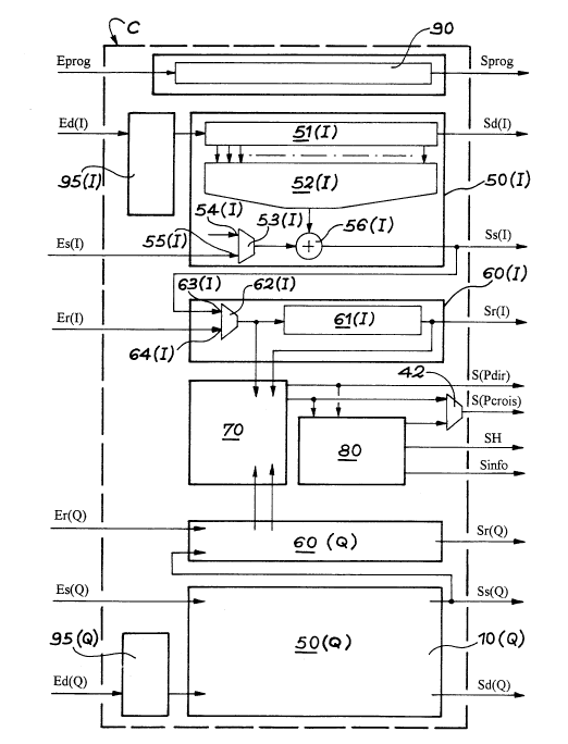
The general structure of the circuit according to the invention is shown in
fig. 4. This circuit comprises two similar channels, one processing the
in phase part I and the other the in quadrature part Q. The references of
the means constituting these two channels are followed by I or Q, as a
function of whether they belong to the first or second channel. This circuit
also has seven inputs, namely three inputs for the channel I (respectively
Ed(I), which is a data input and two inputs Es(I) and Er(I), which are
respectively filtered and filtered-delayed signal inputs), three inputs for
the channel Q (respectively Ed(Q), Es(Q) and Er(Q)) and finally a seventh
input Eprog making it possible to enter programming data.
The circuit also has eleven outputs, namely three outputs for the channel I
- (respective~y Sd(I) for the data, Ss(I) for the filtered signal and Sr(I) for
the filtered-delayed signal), three outputs for the channel Q (namely Sd(Q),
Ss(Q) and Sr(Q)), a direct product or Dot signal output S(Pdir), a Crossed
product or Cross signal output S(Pcrois), a clock output SH, an information
output Sinfo, and finally a programming output Spro.
B 12321.3 RS
21 91 551
-
- 12 -
When the circuit of fig. 4 is the only circuit of the receiver, certain
inputs are inoperative, such as inputs Es(I), Er(I), Es(Q) and Er(Q), as well
as certain outputs such as Spro, Sd(I), Ss(I), Sr(I), Sd(Q), Ss(Q), Sr(Q).
When the circuit is connected in cascade to other similar circuits, the out-
puts of one are connected to the corresponding inputs of the following cir-
cuit, as explained hereinafter relative to fig. 7.
Apart from the inputs and outputs, the general structure of the circuit is
as follows. This circuit firstly comprises a first channel for the digital
processing of the part I in phase with the carrier, i.e. data applied to the
input Ed(I). This first channel comprises:
i) first digital means 50(I) able to fulfil a first filtering function
corresponding to a pseudorandom sequence used on transmission,
ii) first digital means 60(I) able to fulfil a first delay function.
The circuit also comprises a second digital processing channel receiving the
second part Q of the signal received, said second part being in phase quad-
rature with the carrier. In practice, this second channel receives the data
applied to the input Ed(Q) and comprises, like the first:
i) second digital means able to fulfil a second filtering function corres-
ponding to said pseudorandom sequence,
ii) second digital means able to fulfil a delay function.
The circuit in question also has a multiplication circuit 70 incorporating:
- two first inputs, one connected to the output of the first digital filter-
ing means 50(I) and receiving a first filtered signal Ik and the other being
connected to the output of the first means able to fulfil the delay function
61(I) and receiving a first filtered-delayed signal Ik 1'
- two second inputs, one connected to the output of the second digital filter
ing means 50(Q) and receiving a second filtered signal Qk and the other
connected to the output of the second means able to fulfil the delay function
61(Q) and receiving a second filtered-delayed signal Qk 1'
- means for calculating the two direct products between the filtered and
filtered-delayed signals of the first and second channels, namely IkIk 1 and
QkQk 1 and the two crossed products between the filtered signal of one
B 12321.3 RS
- 21 91 551
- 13 -
channel and the filtered-delayed signal of the other channel, namely QkIk 1
kQk- 1 '
- means for calculating the sum of the direct products, i.e. IkIk l+QkQk 1
and the difference of the crossed products, i.e. QkIk 1-IkQk 1-
The circuit of fig. 4 also comprises an integration and clock regenerationcircuit 80 receiving the sum of the direct products and the difference of the
crossed products. The circuit of fig. 4 also comprises a digital programming
circuit 90 containing informations able in particular to program the first
and second filtering means 50(I), 50(Q).
In the illustrated variant, the first and second digital means 50(I) and
50(Q) able to fulfil the first and second filtering functions, incorporate
(only the means of the first channel are shown) a shift register 51(I), an
adder-subtractor 52(I), a gate 53(I) having a control input 54(I) and a
signal input 55(I) receiving a filtered signal from the input Es(I) and a
summating or adding circuit 56(I) having a first input connected to the
output of the adder-subtractor 52(I) and a second input connected to the
output of the gate 53(I).
In the illustrated variant, the first and second digital means 60(I), 60(Q)
able to fulfil the first and second delay functions incorporate (only the
means of the first channel being shown) a multiplexer 62(I) with an input
connected to the output of the summating or adding circuit 56(I) and another
input connected to the delayed signal input Er(I) and a random access memory
61(I) with an input connected to the output of the multiplexer 62(I) and an
output Sr(I) supplying a delayed signal.
Preferably, the two channels also have a first and second shaping and summat-
ing circuits 90(I), 90(Q) placed respectively in front of the first and
second filtering means 50(I), 50(Q).
The digital programming means 90 comprises a shift register having an input
Epro and outputs connected to the first and second shift registers of the
two channels, also connected to the first and second adder-subtractors 52(I)
of the first and second filtering means 50(I), 50(Q), also connected to the
8 12321.3 RS
- 21 91 551
- 14 -
first inputs 54(I) of the first and second gates 53(I) of the first and
second delay means 60(I), 60(Q) and finally connected to the multiplication
means 70 and to the integration means 80.
The circuit of fig. 4 functions as follows. In very general terms, the
informations to be processed are presented to the baseband circuit by the
inputs Ed(I) and Ed(Q). The processings are identical on both channels.
The blocks 70 and 80 combine the baseband data and construct correlation
peaks. They deduct therefrom the binary information corresponding to the
message received. The information is available on the output Sinfo. The
block 90 intervenes in the configuration of the circuit and makes it possible
to fix the different parameters. It has no direct function in data process-
ing.
In a more detailed manner, the block 95 (in other words the block 95(I) for
channel I and block 95(Q) for channel Q) is a summator or adder placed at the
head of each channel. It permits the taking into account of 1 to 5 samples
per chip period. The data taken into account are 4 bit-digitized baseband
raw data at a sampling frequency.
The block 50 (respectively 50(I), 50(Q)) makes it possible to perform the
matched filtering of the data supplied by the head summator. It incorporates
registers for creating an environment able to extend to 128 data items and
adder-subtractors for performing the convolution function. Each data item
is multiplied by a coefficient of the pseudorandom sequence and all the 128
products obtained are summated. The filtering block, to take account of the
cascadable nature of the component, has a supplementary summator 56 (respec-
tively 56(I), 56(Q)) making it possible to recombine the partial result of
the preceding neighbouring circuit (by inputs Es(I) and Es(Q)) with its own
calculation and transmits the result to the following circuit by outputs
Ss(I) and Ss(Q). The informations transiting in these circuits are coded on
8 bits.
The block 60 (respectively 60(I) and 60(Q)) has the function of delaying the
matched filtering result. In the case of a single circuit, the informations
taken into account are those which come from the adder-substractor. The
B 12321.3 RS
21 ~1 551
`~
- 15 -
delay is implemented by means of a random access memory having two inputs,
the first input being used in writing (information to be delayed) and the
other in reading (information delayed), the difference between the two
addresses corresponding to the desired delay. The informations are then
transmitted to the multiplication block 70.
Said multiplication 70 performs a complex multiplication between the result
of the filtering and the same delayed information. The calculations
performed make it possible to obtain a sum of direct products SPD and a diff-
erence of crossed products DPC:SPD = IkIk-1 + QkQk-1
DPC = QkIk_1 ~ IkQk-1
The main operators used for these calculations are four 8 bit multipliers and
two adders. The results are reduced to a 10 bit dynamics.
The block 80 permanently scans the data transmitted by the block 70 on the
output S(Pdir). It detects and follows the correlation peaks in order to
record a clock Hinfo timed to the symbol frequency Ts. It integrates the
sum signal of the direct products in a time range centred around the strong-
est amplitude peak in order to produce the binary data item representing the
information, which appears on the output Sinfo.
The configuration of the general circuit is assumed by the block 90. The
different parameters, such as the sequence length, the binary coefficient
values of the pseudorandom sequence, the cascading of the calculating units,
the control of the complete data paths and the integration time are configur-
able. A shift register of e.g. 253 bits contains the appropriate informa-
tions. This register is loaded prior to the use of the circuit. The con-
figuration bits are presented in series by the input Eprog.
Fig. 5 shows an embodiment of the integration and clock regeneration circuit80 incorporating a detection means 100, a clock regeneration means 102 and an
integration means 104. The circuit 80 has two first inputs ESpD and EDpC
receiving from the circuit 70 respectively the sum of the direct products or
Dot and the difference of the crossed products or Cross. The circuit 80 also
B 12321.3 RS
21 91 551
- 16 -
has two reference inputs, respectively Ecl and Ec2, which receive from the
circuit 90 informations concerning the start of integration and the inte-
gration length. The circuit 80 has two outputs, namely SH supplying a clock
signal and Sinfo supplying the restored information.
The means 102 essentially comprises a counter 103 incrementing on each chip
period (Tc). The ni u~ counter value is set either to 0, or to 1, or to 2.
The capacity of the counter corresponds to the total number of chips in a
sequence, in other words to the length of the sequence, i.e. lseq. The dura-
tion of this sequence is Ts.
When the ni . counter value is fixed at 1, the counter period is preciselyTs, the period of one symbol. The setting of the ini value different
from 1, namely at 0 or 2, makes it possible to increase or decrease the
counter period by a chip period, i.e. Tc. When the counter content passes
through all the values from 0 to lseq, the counter period is equal to Ts+Tc.
When the counter content passes from 2 to lseq, the period is equal to Ts-Tc.
When the counter content passes to the maximum value lseq, a signal H passes
from 1 to 0 (falling front). When the counter content passes to half the
~xi content, i.e. lseq/2, the signal H passes from 0 to 1 (rising front).
Fig. 6 illustrates this operation with, at the top, (a) the variation of the
counter content as a function of the number of chips received and, at the
bottom (b) the clock signal H.
The means 100 make it possible to follow the correlation peak and essentially
comprise a comparator 110 and a register 112. The comparator 110 makes it
possible to detect a high amplitude peak in a range corresponding to the
symbol half-period (Ts/2).
The position of the peak relative to the rising front of the clock signal H
will make it possible to set the counter 103 by adding or subtracting 1 with
respect to the smallest value of the counter.
As the sliding of the rising front of H with respect to the detected peaks
takes place at a rate of one chip period (Tc) per symbol period (Ts), the
B 12321.3 RS
- ` 21 91 55 1
- 17 -
~ x; I synchronization time necessary is defined by the product of Ts by the
number of chips per half-symbol.
The restoration of the data item takes place by the means 104, which essen-
tially comprises an accumulator 114. Accumulation takes place from the
moment where the value of the counter 103 producing the clock H is equal to
the signal marking the start of integration (input Ec1). Accumulation is
activated when the value of the counter generating the clock H is below the
sum of the signals indicating the start of integration and the length of
integration (input Ec2). Once accumulation is ended, the sign of the accumu-
lated data item determines the value of the information which will be trans-
mitted on the next rising front of H. If the accumulation result is negative,
the information will be equal to 0, otherwise the information supplied will
be equal to 1.
A sync signal can indicate that there is synchronization between the high
amplitude peaks and the integration range, i.e. that the binary information
from the accumulation is significant.
Fig. 7 illustrates the case where three identical circuits are connected in
cascade, i.e. C1, C2, C3. The inputs of the first circuit C1 receives the
data I and Q of the signal by their inputs Ed(I) and Ed(Q). The outputs of
this first circuit C1 are directly connected to the corresponding inputs of
the second circuit, i.e. C2. In the same way, the outputs of C2 are conn-
ected to the corresponding inputs of C3. Only circuit C3 has activated multi-
plication circuits 70 and integration circuits 80, the other circuits C1 and
C2 having their corresponding means inactivated. In the same way, in the
circuits C1 and C2, the gate 53 is open, so that chaining takes place between
the adder 56 and the output of the filtering means of the preceding circuit.
The last circuit C3 is the only one to have the final result concerning
filtering. This result appears on the outputs Ss(I) and Ss(Q) and these
results are reinjected into the first circuit by the inputs Es(I) and Es(Q).
The delay blocks 60 are also chained and form a delay corresponding to all
the sequences placed end to end.
With regards to the summating means 95, only the means of the first circuit
B 12321.3 RS
21 91 551
- 18 -
Cl are used, the other means of the other circuits C2, C3 being transparent.
For three circuits, each operating on 128 chips, the entity operates on a
sequence of 384 chips (3 x 128).
NaturaLly, the invention is not limited to the cascade connection of three
circuits, but can instead cover any random number of circuits. It is also
not limited to 128 chip sequences, but can instead use sequences of a random
length.
B 12321.3 RS