Note: Descriptions are shown in the official language in which they were submitted.
-1-
SYSTEM FOR DISPLAYING CALLIGRAPHIC
VIDEO ON RASTER DISPLAYS
BACKGROUND OF THE INVENTION
1. Field of the Invention. The present invention relates to video
graphics and more particularly to a system and method for processing analog
calligraphic video signals to convert them into digital data suitable for
presenting stroke images on a raster display device such as a flat panel LCD
display.
2. Problem to be Solved. Calligraphic video signals consist of a
series of analog voltage signals indicative of X, Y, and Z components which
may be used to produce an illuminated track or stroke on a display surface,
such as the phosphor screen of a cathode ray tube (CRT). In a CRT, an
electron beam illuminates the phosphors and in an XYZ CRT monitor the
calligraphic signals are usually encoded for direct use in controlling the
beam.
Each X component is indicative of an X-deflection of the beam, i.e., a
horizontal position on the screen, while each Y component indicates a Y-
deflection or a vertical position on the screen. Each Z component is
indicative
of the brightness to be produced by the beam at the position defined by its
coordinated X and Y components. A stroke image is thus produced by
appropriately controlling the successive X, Y, and Z component combinations
to produce an illuminated track on the screen.
While a CRT monitor can use the analog calligraphic signals directly,
video displays typically use a raster scan system and XYZ calligraphic analog
voltage signals cannot be used by a raster system without conversion. In a
raster display, to form an image the beam is regularly swept from side to side
across the surface of the screen in a raster action beginning at the upper
left
hand corner and proceeding in a series of successive lines to the bottom of
the
screen. The beam is then returned to the upper left hand corner to begin the
next sweep. During the sweep, the Z component signals produce illuminations
-2-
at successive positions in each line. Each illumination is indicative of the
brightness to be produced by the beam at the respective positions defined by
the Z component's coordinated X and Y components. Each image is thus
formed by the series of illuminations along the prescribed raster lines in
keeping with the successive X, Y, and Z component combinations. For such
an operation it is convenient to use a frame buffer memory for storing the Z
component signals digitally at addresses indicated by their respective X and Y
coordinates. The contents of the buffer memory can then be used to
appropriately control the illumination of the phosphors of the pixels of the
display to create the succession of images defined by the video input signals.
In a typical video raster display, the beam after each sweep is returned
at zero intensity to begin the sweep for the next image. In some applications,
for example, in avionics displays, the intensity and the position of the beam
have been controlled during the return to produce a form of overlay on the
raster video image displayed. This overlay is what is referred to as a
"stroke"
or "stroke image" and is determined and controlled by analog voltage inputs of
calligraphic video signals. Currently, in avionics applications flat panel LCD
displays are replacing the conventional phosphor screen display with the
attendant desirability of digital processing of the video signals since such
displays conveniently use previously-mentioned frame buffers in the form of
digital memories with each memory location in a buffer representing a
location corresponding to a pixel on the display screen surface. The digital
frame buffer contents are periodically transferred to produce a successive set
of images on the display surface in accordance with successive sets of digital
data supplied to the buffer. It is therefore necessary to convert the
successive
sets of calligraphic analog voltage signals to successive sets of digital data
in
the frame buffer, which data is transferred as pixel exciting signals to
produce
the distinctive illuminated strokes on the display for the overlay formation
on
the video images.
Although analog to digital conversion is normally straightforward and
can be readily applied to video raster scan conversion, effective stroke scan
~~916~7
-3-
conversion requires a different approach. Stroke symbology by its nature has
a much higher resolution than conventional video and also must be presented
with high quality anti-aliasing. Therefore, simple digitizing and storing of
stroke symbology in a frame buffer would not only require a very large frame
buffer to maintain the resolution, but additionally the scan conversion rate
required to scale the stroke to an appropriate size to match the display size
would be very high. Currently, memory components are not commercially
available that can handle the requisite high speed. Further, other conversion
artifacts must be considered, such as noise quantization, wherein small noise
levels in the X and Y deflection signals can be magnified to full pixel
position
variation, and clock fitter quantization, wherein the apparent end points of
the
lines can vary by a pixel in a rhythmic manner due to beat frequencies
between the display generator digital-to-analog (D/A) clock and the local
analog-to-digital (A/D) clock.
3. Objects of the Invention. it is accordingly an object of the
invention to convert XYZ calligraphic video signals to be presented as a
stroke image on a raster display to digital data stored in a conventional
frame
buffer for the display.
It is a further object of the invention to provide a system and method
for converting calligraphic video analog voltage signals to corresponding
digital data capable of storage in a frame buffer from which it is used to
produce high resolution graphic images on a raster display.
It is another object of the present invention to provide a system and
method for digitally processing calligraphic video signals for suitable
storage
in a frame buffer and high resolution presentation on a raster display.
It is also an object of the invention to provide a system and method for
converting calligraphic video analog voltage signals to corresponding digital
data capable of producing high resolution, anti-aliased, stroke images an a
flat
panel LCD raster display.
CA 02191617 2002-03-25
-4-
SUMMARY OF THE INVENTION
The present invention involves a system and method for processing
analog voltage signals, that are representative of calligraphic video images
to
be presented on a raster cli~~play screen, by converting such signals to
digital
data in a stroke frame buffer, which data is appropriately processed for
periodic transfer to the display screen to produce graphic video images
thereon. The stroke frame buffer, i.n the form of a digital memory, stores the
digital data in a manner suitable for displaying it as a corresponding stroke
image in a raster display by storing the data at addresses in rows and columns
corresponding to pixel locations on the surface of the display screen. The
analog signals consist of sets of X, Y, and Z components of a calligraphic
image, i.e., the horizontal and vertical locations of each point on the
display
screen making up the image track c>r stroke, and the respective color
brightness of each of the points. In terms of the raster, each X component is
indicative of an X-deflection of the beam, i.e., the horizontal position of a
stroke point on the screen c:.orresponding to the point of intersection of the
beam and a pixel on the surface of the screen. More than one point may fall
within one pixel. Each Y component is indicative of a vertical deflection of
the beam or, in other words, the raster line which is to contain the stroke
point
defined by the X component in its set. Each Z component indicates the
intensity of the stroke point at the screen location defined by the X and Y
components of its set and contributes to producing a corresponding color
brightness of the pixel at that location on the screen.
In accordance with the invention, the problems posed by the high scan
conversion rates and large frame buffer sizes that would be required when
using conventional conversion techniques are overcome by digitizing the
stroke intensity data to a fractional, e.g., 1/4, pixel resolution through
storing
fractional bits from the X and Y digital deflection data in the stroke frame
buffer along with the color intensity data. further, the noise and clock
conversion artifacts are minimized by saving the data for the first and last
point of each stroke line or vector and by using the X and Y fractional bits
for
~~ 9 ~ 6~7
-5-
beam shaping utilizing anti-aliasing discs. The discs are a set of prestored
circular intensity profiles, e.g., 16, each covering several pixels and
corresponding respectively to 16 sets of X and Y fractional bits, so that any
variation in intensity is limited to a 1/4 pixel, which is not detectable by
the
human eye. The data output from the stroke frame buffer is shaped by the
disc data in presenting the stroke image on the raster display.
Accordingly, analog signals indicative of coordinated sets of X, Y, and
Z components are input through appropriate preamplifying and filtering
circuitry to respective analog-to-digital (A/D) converters and the digital
output
signals are stored, after processing, in a stroke frame buffer memory and in a
raster frame buffer memory. The digital output signal corresponding to the X
component in a set defines a column address in the buffer, while the Y
component signal of the set defines a row address in the buffer. The
corresponding Z signal determines the digital value of the brightness that is
stored at the row and column address defined by the respective X and Y
signals. The video Z signal has four components (R, G1, G2, B), which are
stored in the raster frame buffer memory, and the stroke Z signal has three
components (R, G, B), which are stored in the stroke frame buffer memory.
Fractional bits from the X and Y signals, i.e., the two least significant
(LSB)
X and Y bits, are also stored with the brightness digital value in the stroke
frame buffer memory. Successive sets of analog signals are converted by the
A/D converters to digital data in the frame buffers in this manner until the
buffer memories are appropriately filled. The data in the two buffers is
periodically transferred under the control of a suitable sequencer, with the
stroke frame buffer data being shaped by the profile technique, for display on
the raster display device during the raster sweep. The resulting image is a
graphic video image overlaid on the video image produced during the raster
sweep. Ping-gong memories are used in the buffers to facilitate rapid transfer
and the system is provided with appropriate anti-aliasing circuitry,
filtering,
and clock signal generating and coordinating means to achieve optimum
images and operation.
CA 02191617 2002-03-25
_(_
BRIEF DESCRIPTION OF THE DRAWINGS
FIG. 1 is a block diagram of a system for processing XYZ analog
signals to convert them to digital data for storage in a frame buffer memory
and use in presenting a stroke graphic image on a raster display device in
accordance with the present invention.
FIG. 2 is a block diagram in greater detail of the input processing
components and A/D converters of the system of FIG. 1.
FIG. 3 is a block diagram for the timing and control circuits of the
raster scan converter and stroke scan converter for controlling the raster and
stroke scan signals in implementing the control circuitry of the system shown
in FIG. 1.
FIG. 4 is a schematic of raster frame buffer and stroke frame buffer
memories with the associated control circuitry for producing video and stroke
images on a LCD display.
FIG. 5 illustrates a matrix of 16 disc profiles with 2 exemplary
shadings that may be used in line anti-abasing.
FIGS. 6A, 6B and tiC illustrate a series of steps in which the profiles of
FIG. 5 are used for anti-aliasing.
DETAILED DESCRIPTION OF THE PREFERRED EMBODIMENT
The preferred embodiment of the present invention will be described in
terms of the use of A/D flush converters and a flat panel LCD raster display
with a quad pixel arrangement, but it will be understood that many of the
described components in the system and features in the method set forth may
be substituted for and other alterations may be made by those of skill in the
art within the scope of the invention.
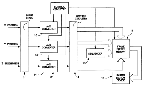
A block diagram of a system for processing sets of calligraphic analog
XYZ signal voltage inputs in accordance with the invention is shown in FIG.
1. The system is incorporated into the circuitry of a raster video device,
such
as an avionics video display, and generally comprises an input stage I, for
receiving X position, Y position, and brightness (Z) indicative analog voltage
CA 02191617 2002-03-25
signals in coordinated sets, and a converter stage 2 with respective A/D
converters 10, 12 and 14. The calligraphic analog signals, as well as signals
indicative of a video image to be displayed, are converted by the respective
A/D converters into digital data that are processed in mapping circuitry 3 to
produce signals indicative of a column address, a row address, and a
brightness value in a frame buffer memory component 1 1 to which the signals
are supplied. Alternatively, the brightness signals may be converted by an
ON/OFF comparator, rather than an A/D converter, if the strokes to be
produced on the display area of a monochrome on/off type. The contents of
the frame buffer memory component 11 are periodically output under the
control of a suitable sequencer 13 to a raster display device 15 for
displaying
a corresponding video image and overlaid stroke or graphic image on its
screen. In the preferred embodiment the display screen is a flat panel, color,
active matrix LCD display (AMLCD) with a quad pixel arrangement.
The input stage and A/D converters are shown in greater detail in FIGS.
2A and 2B. As seen in FIG. 2A, the X and Y deflection signals of a
set, which are input from a switching ramp circuit card assembly in the video
device (not shown), are processed through differential buffers 21x and 21y and
low-pass filters 22x and 22y of the deflection/dimmer 20, also on a circuit
card assembly (CCA), to respective current drivers 23x and 23y. The current
drivers 23x and 23y feed the processed analog signals to X and Y A/D
converters l0a and 12a, preferably 12-bit A/D flash converters, provided with
feedback error amplifiers 24x and 24y. The outputs of the flash converters are
12 bit digital signals indicative of the X and Y positions in a frame buffer
memory for storage of the illumination value indicated by the Z signal of the
set. A deflection clock 2..5 :is provided in the deflection/dimmer circuitry
20
for producing a clock pulse to coordinate the timing of the outputs of the
converters l0a and 12a.
As shown in FIG. 28,, the Z stroke (for a
monochrome stroke) signal is processed along the green video data in raster
scan converter circuitry 4() on a CCA containing switching circuitry 26,
CA 02191617 2002-03-25
_g_
elliptical filters 27a, 27b and 27c, and current drivers 28a, 28b and 28c.
Since
the output images for description purposes are to be displayed on an AMLCD
display with a quad pixel arrangement, it will be noted that the Z signals
representing three color (RGB) strokes are input via the red, green and blue
stroke signals to the switching circuitry 26. 'The input signals include red
and
blue and green stroke and green video signals from a switching ramp CCA,
and red and blue video signals from an encoder CCA. The processed analog
outputs in green, red, and blue sets are fed from the current drivers (28a,
28b,
28c) to A/D converters l4ar, l4ag, 14b, and 14c, preferably 7-bit A/D flash
converters, each having a mapping programmable read-only-memory (PROM)
29ar, 29ag, 29b, and 29c, at its output. For AMLCD display purposes, it
will be noted that an additional A/I~ converter l4ar is provided in one
circuit
leg, and that this converter along with its mate l4ag, have respective RG2 and
BG1 clock inputs, while converters 14b and 14c respectively have the same
clock inputs. The four digital output signals G2, G1, R, and B, to be used to
drive the LCD display, are fed in the form of a 24 bit signal (6 bits per
color)
to a brightness bus 31 for input to raster scan converter circuitry 40,
and in the form of a 12 bit I~GB signal, along with the 12 bit X and Y
position signals, to stroke scan converter circuitry 30 (see FIGS. 4A and 4B).
The 12 bit position signals X and Y are fed to a start pixel detection
circuit 32 and the 12 bit brightness signals Z to a stroke brightup generator
33
(See FIG. 3A), both of which devices are controlled by a green video
clock/deflection clock signal from a phased clock generator 34, with a
programmable clock delay, in the deflection/dimmer circuitry 20. Phased
clock generator 34 also outputs red and blue video clock signals. The start
pixel detection circuit 32 outputs a start point protect signal that functions
to
specifically preserve the starting point of each stroke line, by saving the
point
in storage, to minimize jitaer for anti-abasing purposes. The stroke brightup
generator 33 generates a stroke bright-up signal for disabling stroke writing
to
memory during blank stroke, stroke beam repositioning, and raster graphics.
A start point protect signal and a stroke brightup signal from the respective
CA 02191617 2002-03-25
_g_
devices, 32 and 33, are fed to a stroke update controller 35 (see also FIG.
3B),
which also receives a green video clock/deflection clock input from the phased
clock generator 34 as well ~~s raster,~stroke and stroke sync signals, the
latter from
a cathode reset detector 18 in the video device. The output of the stroke
update
controller 35 is provided to a stroke frame buffer control multiplexer 36,
along
with a ping/pong swap coni:rol signal from the deflection/dimmer circuitry 20
and an LCD/stroke Read/VVrite PAM control signal from an LCD controller 37
in the raster scan converter CCA 40. The stroke frame buffer control
multiplexer
36 outputs stroke ping control signals sp 1 and stroke pang control signals
sp2 to
a stroke frame buffer 43 which contains a ping~pong memory (43a and 43b)
as shown in FIG. 4A.
The ping/pong frame buffer configuration allows one half of the buffer
memory to be dedicated to updating stroke graphics while the other half is
being read to generate data to refresh the display. Typically the ping/pong
memories are swapped at a 30 Hz rate under control of the raster scan
converter circuitry 40 anc:l the LCD display is updated at a 60 Hz rate. With
an AMLCD display, however, the display is driven with the same data for two
consecutive fields (field :L/field 2) t:o allow the display drivers to reverse
the
drive polarity between fiE:lds in order to eliminate DC plating effects on the
AMLCD glass. In such 4~ case, every other stroke field is discarded and the
display update rate is 30 H:z.
A video update controller 38, shown in FIG. 3B, is also part of the raster
scan converter circuitry 40 and receives the raster/stroke and stroke sync
signals as well as field 1/field 2, horizontal and vertical blanking signals
and a
green video clock/deflection clock signal from the phased clock generator 34.
The output of the video update controller 38 consists of a 9 bit video address
X signal and a 10 bit video address Y signal, which are fed through a +1
adder circuit and address multiplexer 42 to the ping-pong memories 41a and
41b of raster frame buffer 41 (see FIG. 4B), and of a video write RAM control
signal, which is input to r~ raster frame buffer control multiplexer 39. There
is
also an output from controller 38 to a microcontroller data bus 50. The raster
CA 02191617 2004-04-27
-10-
frame buffer memories control multiplexes 39 which outputs a video ping
control
signals VP 1 and video pong control signals VP2 to raster frame buffer 41 a
and
41b. The LCD controller 37, which receives a ping-gong swap control signal
from a controller 17 and an LCD pixel clock signal from an LCD pixel clock
generator 51 (see FIG. 3A), as well as an input from the microcontroller data
bus 50, outputs a 9 bit LCD scan address X signal and a 9 bit LCD scan address
Y signal to an address multiplexes 44 (see FIG. 4) which provides 9 bit X and
Y
addressing inputs to the stroke frame buffer ping-gong memories 43a and 43b.
As seen in FIG. 4A and in accordance with the invention, respective 11
bit signals on the X position bus and the Y position bus have their 9 most
significant bits (MSB) input to the address multiplexes 44 and their 2 least
significant bits (LSB) input to the data multiplexes 43c. The 9 MSB bits are
representative of the X and Y position of the pixel to be illuminated and the
fractional 2 LSB bits are indicative of the location within the pixel. The
multiplexes 44 uses the 9 X and Y digitized deflection MSB bits to address a
memory location in each of the ping-gong memories, 43a and 43b, in stroke
frame buffer 43.
The 24 bit signals on the brightness bus 31 (see FIG. 4A) have 12
bits input, along with the previously-mentioned sets of 2 LSB bits from the X-
position and Y-position busses, to data multiplexes 43c, which in turn
provides
16 bit inputs for storage in the locations in stroke frame buffer memories 43a
and 43b. The 12 MSB bits of the 16 bit input include 4 bits to respectively
indicate each of the three color (RGB) brightnesses for a given pixel, while
the 4 LSB bits are used to determine where within the illuminated pixel the
indicated brightness is to occur in a manner providing 1/4 pixel resolution as
will be described below.
Each buffer memory, 43a and 43b, may have a 512 x 512 memory
array with 16 planes. As the RGB stroke intensity data comprises 4 bits for
each color being written to a memory location along with the two lowest
(LSB) X and Y position bits for that location, the 512 x 512 memory with the
fractional position bits results in an effective 2048 x 2048 stroke
resolution.
~19i6~7
-11-
Thus improved stroke resolution is obtained using a conventional sized buffer
memory, and each location in memory corresponds to a pixel color group on
the LCD display.
The improved resolution is combined with improved anti-aliasing
through the use of a shading profile disc generator in a manner as will now be
described.
A display pixel may be considered to be divided into 16 locations or
points. Preferably the stroke data will be digitized at least four points per
pixel on the display. As each storage location within the frame buffer
memory corresponds to one pixel on the display, one of the four digitized
points will be selected for storage and the others discarded. In accordance
with the invention, the first point of a stroke line is selected and its data
is
saved, and any other points within the pixel in which the first point is
located
are discarded. In subsequent pixels, the data of the last point within the
pixel
is stored and previous stroke line points in the pixel are discarded. Of
course,
if the stroke line to be formed has only one point within a given pixel, then
the data of that point will be stored to identify the brightness value for
that
pixel. Thus, each pixel will have a digital color brightness value stored in
its
buffer memory location indicative of the brightness at one of the 16 points
making up the pixel. As the timing of the successive display of the pixel
points can cause movement and distortions in the stroke line actually
displayed
(abasing), to achieve anti-abasing a set of shading profiles is used that
consist
of 16 prestored profiles containing various pixel grids that preferably will
provide a Gaussian profile for the displayed line.
More particularly, to allow for the fact that a line can be drawn at any
angle across the display, the shading profiles are stored in circular or disc
form and each extends over or covers a number of square pixels. The discs
should have profile centers that correspond as accurately as possible to
points
on the ideal (mathematical) center of the stroke line, so that a number of
circles may be predetermined using, for example, centers offset in the X and
Y direction by fractions of a pixel spacing, that is, the center offsets may
be 0,
CA 02191617 2002-03-25
-12-
1/4, ~/z, and 3/4 of a pixel in both the X and Y directions. In any event, 16
circular intensity maps in the form of 4x4 pixel grids, such as shown in FIG.
5, may be prepared containing intensity codes that result in a circular
profile,
for example, Gaussian, linear, or any desired template. The center offsets are
indicated in the figure by an x in each grid and the numbers in the pixels
correspond to relative shadings. The two profiles at the top of the figure
illustrate exemplary disc shadings. 'These profiles, respectively
corresponding
to the 16 point locations within a pixel, are stored for use in a disc
generator
during the processing of the data in the stroke frame buffer 43. That
processing is as follows.
The LCD controller 37 (FIG. 3B), which implements the function of
sequencer 13 in FIG. l, pravides a read address signal to a disc generator
that
includes, for example, a CJaussian disc PROM 4~ (FIG. 4B), in
combination with circuitry 48 (FIG. 4A), consisting of two application
specific
integrated circuits (ASICs) 48a and 48b with associated FIFO memories 48c
and 48d, that takes part in processing the stroke pixel signals using data
directly input from the stroke frame buffer 43. The disc PROM 45 stores the
predetermined circular or disc profiles that will be appropriately selected
and
assembled to create the stroke line image on the display. The read address
signal causes the 16 profiles to be downloaded from PROM 45 to the ASICS
48a and 48b. The fractional X and Y bits and the RGB color intensity data
indicative of the points of a stroke line are fed from the stroke frame buffer
memories 43a and 43b in sequence left to right and top to bottom to the
ASICs 48a and 48b.
The predetermined circular intensity profile or disc with its center
related to or nearest each digitized point retrieved from the frame buffer is
then copied into an nxn memory within the ASICs. This corresponds to an
nxn grid area around each pixel. Then, as shown in FIG.6B, processing of the
digital point intensity data is continued and, at each pixel, the last point
indicated by the digital data signals is selected and the previous point data
for
that pixel discarded.
CA 02191617 2002-03-25
-13-
When, during processing, a subsequent disc is selected which has a
pixel in its profile that overlaps a pixel from a profile previously copied
into
memory, the two pixel intensities are compared and the one with the larger
value is retained in memory and the smaller value is discarded (this is called
a
MAX function).
The disc profiles are thus successively loaded in overlapping
relationship into memories 48c and 48d as square pixel arrays and the profiles
repeatedly generated (Fig. fiB), using a maximizing algorithm (MAX function)
which ensures that the brighter points are retained along the ideal center of
the
stroke line until the end of the line is reached. An example of the resulting
line shading is illustrated in FICA. 6C.
As mentioned above, the first or starting point of the line is selected
and saved to be indicative of the brightness of the pixel in which it is
located,
which is the pixel with its center closest to the starting point. As shown in
FIG. 6A, the line ends can be positioned on a .sub-pixel grid.
The application of this mode of operation in the system of the invention
makes it possible to form a high resolution, anti-aliased line on a flat panel
LCD display that is nearly :identical to a stroke line on a CRT. Consequently,
the disc generator (PROM 45 and circuitry 48) functions in the manner of a
filter which shapes a beam, micropositions the beam to within 1l4 pixel and
covers several pixels so that any positional variation in intensity is limited
to a
1J4 pixel. This technique also ensures that crossing lines blend smoothly and
lines can be anti-aliased to any color or video background.
Returning to the system shown in FIGS. 4A and 4B, it will be seen that all 24
bits
on the brightness bus 31, representing the R, G1, B, and G2 signals (FIG. 1)
are input to a data multiplexer 41c, which provides inputs to raster frame
buffer memories 41 a and 41 b. The data multiplexers 41 c control which side,
the ping memory (41 a) or the pong memory (41 b), accepts the brightness data.
The raster frame buffer 4 I. may have 512 x 1 ()24 positions in each memory
with 4 six bit planes for the R, G 1, G2, B colors.
CA 02191617 2002-03-25
-14-
The outputs of the raster frame buffer 41 are coupled through a data
multiplexer 41 d to a bilinear or interpolation circuit 46 that is part of an
ASIC
and which feeds raster pixel or video signals to a stroke/raster mixer 47 that
is
part of a gate array. The outputs of the stroke scan frame buffer 43 are
processed through ASICs 48a and 48b and memories 48c and 48d, as
explained above, which in turn provide stroke pixel signals to the
stroke/raster
mixer 47. The output of the mixer 47 is fed to an LCD data flow controller
49 which provides the appropriate LCD pixel signals to an LCD raster display
device 15 (FIG. 1 ) based on the raster and stroke pixel signals input to
mixer
47. A video image having a stroke image overlay results on the display.
Additional system components to facilitate the rasterization of the two
images are also shown in F1G. 4B. Respective 11 bit signals on the X position
bus and the Y position bus are input to a raster system controller unit 53
which contains a number of raster system components, such as ramp startlstop
registers that produce an output to a raster sealer and translator sync
processor,
a mieroeontroller, and a c~andom access memory and EPROM. Controller unit
53 additionally receives an input from microcontroller bus 50 which is also
input to a transceiver 54 that is part of the stroke scan converter circuitry
30
and receives an input from the disc generator.
The raster system cc.~ntroller unit 53 also receives raster/stroke, V drive,
H drive, raster blanking, and backup video clock inputs and outputs a 2X
video clock signal to phase clock generator 34, field '/2, hblank, and vblank
signals to video update controller 38, and microcontroller control signals, in
running the raster system to produce the video image.
It will therefore be seen that a system and method are disclosed for
converting analog XYZ calligraphic video signals to digital data that can be
suitably stored in a conventional sized buffer memory and used to produce a
high resolution, anti-abased stroke image which image may be overlaid on a
conventional video image, .and displayed on a flat panel LCD raster display.