Note: Descriptions are shown in the official language in which they were submitted.
-- 2 1 ~ 1 9 1 6
THERMAL IMAGING DEVICE WITH
SCANNED LIGHT EMl~ G DIODE DISPLAY
BACKGROUND OF THE INVENTION
Field of the Invention
The present invention is in the field of imaging
devices. More particularly, the present invention relates
to devices for receiving invisible infrared light from a
scene, and for providing a visible-light image replicating
the scene.
Related TechnoloqY
Night vision devices have been available for many
years. One category of these conventional night vision
devices uses image intensifier technology. This
technology is effected using a device generally known as
an image intensifier tube. The image intensifier tube is
essentially a frequency-shifting and amplifying device
receiving ambient light, which light may include visible
light too dim to provide natural vision (i.e., so-called
"Star Light" scopes), or invisible near-infrared light, in
a first frequency band and responsively providing a
greatly intensified visible image in a phosphorescent
monochrome yellow-green light.
~191~16
Such an image intensifier night vision device
converts available low-intensity ambient light to a
visible image which a human user of the device may use for
surveillance or weapon aiming, for example, under lighting
conditions of too dim to allow a scene to be viewed with
the natural vision. These image intensifier night vision
devices require some residual light, such as moon or star
light, in which to operate. This light is generally rich
in near-infrared radiation, which is invisible to the
human eye. The present generation of night vision scopes
use a photoelectrically responsive "window", referred to
as a photocathode, which is responsive to the dim or
invisible ambient light focused on this "window" from an
invisible scene to provide a pattern of photo-electrons
flowing as a space charge moving under the influence of an
applied electrostatic field, and replicating the scene
being viewed. This pattern of photo-electrons is provided
to a microchannel plate, which ampllfies the electron
pattern to a much higher level. To accomplish this
amplification at the microchannel plate, the pattern of
photo-electrons is introduced into a multitude of small
channels (or microchannels) which open onto the opposite
surfaces of the plate. By the secondary emission of
electrons from the interior surfaces of these channels a
shower of electrons in a pattern corresponding to the
low-level image is produced. The shower of electrons, at
an intensity much above that produced by the photocathode,
is then directed onto a phosphorescent screen, again by
the application of an electrostatic field. The phosphors
of the screen produce an image in visible light which
replicates the low-level image.
Image intensifier tubes have evolved from the
so-called "Generation I" tubes through the more recent
"Generation III" tubes, which provide greater
amplification of available light and greater sensitivity
to infrared light somewhat deeper into the infrared
21 911ql6
portion of the spectrum. However, these image intensifier
devices are limited with respect to the depth into the
infrared portion of the spectrum to which they can
operate.
Another category of conventional night vision device
is represented by the cryogenically cooled focal plane
array thermal imaging devices. These devices use a
photoelectrically responsive detector which is cooled to
a temperature in the cryogenic range to reduce unwanted
thermal noise. The detector includes a plurality of
detector elements, or "pixels", each of which provides an
electrical signal indicative of the flux of infrared light
falling on the detector element. Some such devices use a
staring focal plane array; while others have a linear
focal plane array of detector elements, and require the
use of a scanner to sequentially move portions of the
viewed scene across the detector. In either case, because
the detector is cooled to cryogenic temperatures, it can
proved an electrical response to invisible infrared light
much deeper into the infrared part of the spectrum than is
possible with the image intensifier devices. The
electrical signal provided by such a detector must be
processed and converted to a visible image. For this
purpose, many such devices of this category have used
cathode ray tubes, liquid crystal displays, and other such
display technologies to provide a visible image to the
user of the device.
A significant disadvantage of this category of night
vision device is the requirement for cryogenic cooling of
the detector. Early devices of this category used a Dewar
vessel into which a supply of a cryogenic fluid (such a
liquid nitrogen) had to be provided by the user of the
device. The utility of such devices was severely limited
by their requirement for occasional replenishment of the
cryogenic coolant. Later devices of this type have used
cryogenic cooling developed by reverse Sterling-cycle
` 21 919i6
- coolers. However, such coolers require a considerable
amount of power, are not without their own maintenance and
reliability problems, and are generally noisy.
A device of this category is known in accord with
United States Patent No. 4,873,442, issued 10 October 1989
to Robert W. Klatt (hereinafter, the '442 patent). The
device of the '442 patent uses a sensor with a linear
array of elemental detectors each spaced apart from the
next-adjacent detector element by a distance about equal
to the size of the detector elements themselves along the
length of the linear array. Accordingly, the sensor could
capture about half of the image information from a scene
or object space with each field, or scan of the sensor
across the object space. However, in order to detect and
compensate for non-uniformity in responsivity of the
detector elements, the '442 patent teaches to overlap the
scan lines of all of the detector elements in successive
scan fields so that each field is missing image
information from at least one detector element. That is,
no field of the '442 patent uses all of the detector
elements to respond to signal (image information) from the
scene. At least one detector element at one end of the
linear array scans a space outside of the object space and
provides no useful image information. According to the
example set forth in the '442 patent, each field is
missing a fractional part of its maximum possible image
information which fraction is equal to l/n, where n is the
number of detector elements. The remaining n-l detector
elements are used to capture half of the image information
from the object space for each field. Each field thus
presents 90 percent of the image information that it could
contain were all detector elements used. Accordingly,
each frame of two fields of the '442 patent presents a
complete object space image, but represents only 90
percent of the image information which it could provide
were all of the detector elements used in each frame.
2 1 9 1 9 ~ 6
~ Additionally, the possible number of lines of resolution
which the sensor can provide is not fully used by the '442
patent.
The l442 patent does not disclose the device or
method used to display an visible image for the user of
the device. However, conventional devices in the thermal
imaging art have used such display expedients as cathode
ray tubes, which are relatively large, fragile, heavy, and
power-hungry devices. In an attempt to reduce these
negative aspects of the display portion of the device,
some conventional thermal imaging devices have used a
linear array of square or rectangular light emitting
diodes, the light from which is scanned to the viewer by
a mirror system similar to what the '332 patent teaches
for scanning the image space to the infrared detector.
These conventional display devices, which have used
rectangular or square LED's, might be considered as
scanned-LED type of devices.
A disadvantage of these conventional scanned-LED
display devices is that the imagery provided to the user
is replete with one or more of flickering, horizontal or
vertical scanning lines (i.e., visible raster lines in the
display imagery), or other visible artifacts of the
operation of the display device itself. These display
device problems generally include visually distinguishable
features which are not part of the scene being viewed
(i.e., persistent or spurious vertical or horizontal lines
not present in the scene; a persistent horizontal line of
which could easily be mistaken for the horizon, for
example), and which can decrease the performance of the
imaging device and are distracting to the user of the
device. Because the performance of a thermal imaging
device is affected strongly by the quality of the display
device presenting the imagery to the user, many
conventional devices have been compromised in their
performance because of the limitations of the conventional
2t91916
~ 6
- scanned-LED displays. That is, the range performance of
the device may be decreased. Also, a standard test of
thermal imaging devices is set forth in the U.S. Army's
FLIR-90 standard for thermal imaging devices.
The FLIR-90 s~n~rd uses as a thermal resolution
test for a thermal imaging device a group of four parallel
bars, each with a four-to-one length to width ratio, and
each spaced by its own width away from the next bar of the
group. This group of bars is heated to a temperature
above ambient background, and may be oriented with their
length horizontal, vertical or on a diagonal. The minimum
temperature difference of the bars above ambient
background temperature which allows the bars to be
distinguished from the background is referred to as the
minimum resolvable temperature (MRT) for a thermal imaging
device. A low MRT is a desirable indicator of performance
for a thermal imaging device. Understandably, a poor
display device will undesirably increase the MRT of a
thermal imaging device.
Another conventional display expedient has been to
use mechanical reticles or reticle injectors to provide a
reticle or other display symbology to the user of such a
device. This approach is mechanically complex, expensive
and heavy. Also this expedient limits the number of
possible symbology displays which can be presented to the
suer of such a device. At the most, two such symbology
displays are available for a user of a conventional
device.
3 0 SUMMARY OF THE INVENTION
Another indication of the performance of a
scanned-LED display is its flatness of visual field. This
means that the raster pattern of the display blends
together so that it is not discernable to the eye.
Additionally, the spurious response of the display must
not be too high, or else an aliased signal produced by the
21~1ql6
raster sampling process will become visible. Thus, the
modulation transfer function of the display must not be
too high. Further, the display must maximize the range
performance of the thermal imaging device, which means
that the modulation transfer function of the display must
not be so low that it degrades the overall performance of
the imaging device. Moreover, it is clear that the MRT of
the imaging device is affected by the MTF of the display
device, and that the MTF must be as high as is practicable
without causing false visual artifacts in the visual
field. One method of analyzing the modulation transfer
function (MTF) of a scanned LED display is to taking the
Fourier transform of the spatial distribution of the
LED's. The profiles of the LED's in Cartesian coordinates
are considered , and compared for various geometries of
the LED's.
In view of the deficiencies of the conventional
technology, a primary object for this invention is to
overcome one or more of these deficiencies.
Another object for the present invention is to
provide a thermal imaging device having a scanned LED
display which provides a flat visual field, and a
desirably high modulation transfer function enhancing the
overall performance of the thermal imaging device, without
causing spurious visual artifacts in the visual field of
the display device.
According to one aspect, the present invention
provides a light emitting diode (LED) display apparatus
including a linear array of plural spaced apart like scene
light emitting diodes (LED's) defining like spaces between
adjacent scene-LED's, and a scanner scanning light emitted
from the scene-LED's to a viewer with rapid interlacing of
light from successive scans so as to fill in the spaces
between adjacent scene-LED's of the array and to provide
an image, the scene-LED's having a geometric configuration
2 ~ 9 1 9 1 6
- varying in width along a length dimension of the linear
array.
Another aspect of the present invention provides a
thermal imaging device responsive to invisible thermal
infrared radiation from a viewed scene to responsively
provide a visible image replicating the scene, the thermal
imaging device including a detector array responsive to
the thermal infrared radiation and including a
linearly-arrayed plurality of spaced-apart detector
elements defining cooperatively a length dimension for the
detector array, a sc~nn; ng device scAnning the viewed
scene across the plurality of detector elements in a
direction generally perpendicular to the length dimension,
the scanning device on successive scans interlacing
portions of the viewed scene as scanned across the
plurality of detector elements according to the spacing
therebetween to capture image information from all of the
scene, each of the plurality of detector elements
providing a corresponding individual electrical signal
indicative of the thermal infrared radiation incident
thereon, and a display apparatus responsively providing a
visible-light image replicating the viewed scene, the
thermal imaging device including the display apparatus
having a linear array of plural spaced apart like scene
light emitting diodes (LED's) defining like spaces between
adjacent scene-LED's, and a scanner scanning light emitted
from the scene-LED's to a viewer with rapid interlacing of
light from successive scans so as to fill in the spaces
between adjacent scene-LED's of the array and to provide
an image, the scene-LED's having a geometric configuration
varying in width along a length dimension of the linear
array.
These and additional objects and advantages of the
present invention will be appreciated from a reading of
the following detailed description of at least one
preferred exemplary embodiment of the invention, taken in
21~1916
-
- conjunction with the appended drawing Figures, in which
the same reference numeral indicates the same feature, or
features which are analogous in structure or function to
one another.
DESCRIPTION OF THE DRAWING FIGURES
Figure 1 provides a diagrammatic representation of
the functionally cooperating physical components of a
thermal imaging device embodying the invention;
Figure 2 is a schematic block diagram of a thermal
imaging device according to the present invention;
Figures 3a and 3b respectively provide an external
view and an exploded perspective view of a thermal imaging
device embodying the invention;
Figure 4 presents a schematic view of a linear array
sensor utilized in an embodiment of the invention
described herein;
Figures 5a and 5b respectively present a schematic
diagram of the facets of a scanning mirror of a thermal
imaging device embodying the invention, and a chart of
scanning mirror facet angle families, along with
identification of three members of this facet angle family
which have either a facet reference angle or one of a pair
of a transposing facet angles;
Figure 6 is an image space sequential scan chart for
three sequential frames, each having four sequential
fields;
Figures 7 and 8 present related block diagrams
depicting the signal processing circuitry and methodology
used to achieve economical non-uniformity detection and
compensation, as well as global scene brightness level
control in a viewing apparatus according to the present
invention;
Figure 9 provides a schematic diagram of an LED
display structure;
2 ! 9 1 '' I 6
.
Figure 10 is a greatly enlarged view of an encircled
portion of Figure 9;
Figure 11 provides a graphical representation of the
vertical uniformity of the visual field presented by a
conventional display and by a display embodying the
present invention; and
Figure 12 is a greatly enlarged fragmentary view
similar to Figure 10, but showing an alternative
embodiment of the present invention.
DETAILED DESCRIPTION OF AN EXEMPLARY
PREFERRED EMBODIMENT OF THE INVENTION
An overview
Viewing Figure 1, a thermal imaging device 10 is
diagrammatically depicted with its functionally
cooperative physical components suspended in space without
the depiction of a supporting housing (which housing is,
of course, included by a physical embodiment of the
device), so that these components and a ray-tracing
diagram for light rays in the device can also be
presented. Viewing Figure 1 in detail, the thermal
imaging device includes an objective optics group,
generally indicated with the numeral 12. This objective
optics group includes several lenses (indicated with
reference numerals 12', 12", 12"', etc.), which lenses are
transparent to light in the spectral band of interest (but
not necessarily transparent to visible light). The
objective optics group 12 is pointed toward a scene to be
viewed, so that infrared light from this scene (indicated
with the arrowed numeral 14) can be received and focused
by this optics group. It will be understood that the
objective optics group 12 seen in Figure 1 is
representative only, and that this optics group may be
removed and replaced with objective optics of differing
configurations, as will be further described. The
objective optics group 12 concentrates and columnates
2 1 9 1 ~ ~
11
- received light through a window 16, which window is a
permanent part of a basic sensor portion 18 of the device
10. In conjunction with the housing (to be described
below) of this basic sensor portion 18, this window 16
bounds a sealed chamber 20 in which are received almost
all of the remaining components of the device 10 as
illustrated in Figure 1.
Within the housing chamber 20 is received a scanner,
generally referenced with the numeral 22. This scanner 22
includes a scanner frame 24, which is generally of
triangular or tripod configuration in plan view. The
scanner frame 24 includes a generally triangular upper
wall portion 26, and three depending leg portions 28, only
two of which are visible in Figure 1. Carried by the wall
portion 26 is a scanner motor, generally indicated with
the numeral 30. This scanner motor 30 includes a
generally vertically extending rotational drive shaft (not
visible in the drawing Figures) drivingly carrying a
disk-like circular multi-faceted scanning mirror 32. The
scanning mirror 32 includes plural outwardly and
circumferentially disposed adjacent facets or faces 32a,
32b, etc. only a few facets of which are seen in any one
of the drawing Figures. This scanning mirror 32 rotates
in a generally horizontal plane to reflect light 14
received via the window 16 and objective optics group 12
to an image optics group, generally indicated with the
numeral 34. It will be noted that because of rotation of
the scanning mirror 32, the facets 32a, 32b, etc.,
continually change their angulation in the horizontal
plane with respect to the scene viewed via the objective
optics group 12.
Considering the image optics group 34 in greater
detail, it is seen that light (arrow 14) reflected from a
facet of the scanning mirror 32 passes through a lens 36
and to a pair of vertically spaced angulated mirrors 38,
and 40. The mirror 40 reflects this light through an
2 1 9 1 q 1 6
12
- additional pair of lenses 42, and 44 toward a window 46
carried by a Dewar vessel 48. The Dewar vessel 48
includes a thermally insulative housing, generally
indicated with the dashed line and the reference numeral
48'. This Dewar vessel 48 houses a linear focal plane
infrared detector 50 having a linearly-arrayed multitude
of small infrared detector elements, indicated
collectively on Figure 1 with the vertical line 50' on
detector 50. Each of the detector elements 50' of the
detector 50 provides a corresponding one of a like
multitude of electrical signals each of which is
indicative of the flux level of infrared light falling on
the particular detector element. These electrical signals
are provided o~twardly of the Dewar vessel 48 by an
electrical interface (to be further described), and
indicated on Figure 1 with the dashed line 52.
In order to cool the detector 50 to a sufficiently
low temperature that thermally excited electrons (as
opposed to electrons excited by photons of infrared light
falling on the detector 50) do not cause an undesirably
high level of electrical noise which would hide the
desired photoelectric image signal, the Dewar vessel 48
includes a multi-stage reversed Peltier-effect (i.e.,
thermoelectric) cooler 54. The thermoelectric cooler 54
has a chilling face to which the detector 50 is mounted to
be cooled, and a heating face in heat transfer
relationship with a heat sink schematically indicated with
the numeral 56. In the physical embodiment of the imaging
device 10, the heat sink 56 is defined by a metallic
portion of the housing for the device 10 as will be seen.
It will be understood that because of the continuous
change in angulation of each facet 32a, 32b, etc., of the
scanning mirror 32 as this mirror rotates in a horizontal
plane, the scene reflected from each particular facet
sweeps horizontally across the linear array of detector
elements 50' (i.e., perpendicularly to the vertical linear
2 ! 9 1 ~ 1 g
13
array of these detector elements). The detector elements
50' responsively provide electrical signals (via interface
52) which are indicative of the flux levels of infrared
light falling on corresponding ones of the plural detector
elements 50' from a particular part of the scene during
any one sweep of a scene portion across the detector 50.
In order to provide a visible image to be viewed by
a user of the imaging device 10, a light emitting diode
(LED) projection array module 58 is carried by an
apertured flange portion 60 of the scanner frame 26. This
LED projection array module 58 includes a linear LED array
62, which array includes a multitude of individual LED's
(not visible in Figure 1, but indicated with the arrowed
numeral 62'), each individually emitting visible light
when energized. The LED's 62' of the array 62 are arrayed
linearly along a vertical line similarly to the linear
arrangement of the detector elements 50' of the detector
50. The LED's 62' provide respective portions of a
visible image, as will become apparent. Light from the
LED's 62' is columnated and projected by a projection lens
group, generally indicated with the numeral 64, onto a
facet of the mirror 32, and as indicated by the arrowed
reference numerals 14'. The numerals 14 and 14' are used
intentionally with respect to the invisible infrared light
carrying image information from a scene, and the visible
light replicating the scene for viewing by a user of the
device 10.
From the mirror 32 (i.e., from a particular facet 32'
of this mirror) the visible light from the LED's 62' is
reflected to an ocular lens group, generally indicated
with the numeral 66. The ocular lens group 66 includes
several individual lenses, indicated with the respective
reference numerals 66', 66", etc. Along with these lenses
66', 66", etc., a status display unit 68 is interposed in
the ocular lens group 66. This status display unit 68
defines an aperture through which the visible image is
2~ 919l6
14
perceived, and includes several individual LED's which
when illuminating are peripherally visible to the user of
the device 10. These individual LED's are indicated with
the numerals 68', 68", etc. Finally, the imaging device
includes a pair of eyepiece shutters 70. These
shutters 70 are biased closed to prevent light emanations
from the device 10 when a user's face is not pressed
against a movable eyepiece member (to be described below).
When the user presses against the movable eyepiece member,
the shutters 70 open to allow the user to view the visible
light image provided by the LED projection display module
and the spinning mirror 32.
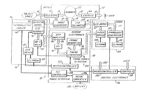
Viewing now Figure 2, a schematic functional block
diagram of the thermal imaging device 10 is presented.
This thermal image device 10 is divided into functionally
modular portions, as is indicated by the dashed-line boxes
encircling the various components of the device, with some
of the modules including several sub-modules or
components. The module 72 manages both invisible and
visible light, and includes the objective optics group 12
receiving the invisible infrared light 14 from a scene to
be viewed, the scanner 22, and image optics group 34
directing this invisible light to the detector 50. This
light management module 72 also receives visible light
from the LED array 62, and includes the projection lens
group 64 projecting this light to the scanner 22, and
ocular lens group 66 providing the image to a user of the
device.
Detection module 74 is enclosed within the Dewar
vessel 48, and receives the focused invisible infrared
light 14 from the scene to be viewed. This module 74
includes the detector 50, along with a readout circuit 76
providing multiple channels of electrical image signal 78
(one channel for each detector element of the linear
detector array 50, recalling the description above) to a
multiplexer circuit (MUX) 80. The MUX 80 provides the
2191ql6
_ 15
- electrical interface output 52 in the form of a serial
analog image signal. Detector module 74 also includes a
driver circuit 82 providing control commands to the
readout circuit 76. An electrically erasable programmable
read-only memory (EEPROM) 84 is included in the detection
module 74 to locally store and provide data on the
operation of the readout circuit 76, providing
compensation factors locally for a number of gain-control
and non-uniformity compensations in connection with the
infrared detector 50. As can be seen from Figure 2, the
various circuits of the module 74 have electrical
interface with other modules of the device 10.
The serial analog image signals 52 provided by module
74 are received by an analog signal processor (ASP) 86
which is located in a process-and-control (P&C) module 88.
A processed serial analog image signal 90 is provided by
the ASP 86 to a analog-to-digital converter (ADC) 92. A
resulting processed serial digital image signal 94 is
provided to a timing generator 96. This timing generator
96 has an interface with the multiplexer circuit 80 to
control the timing of operation of this circuit. A frame
memory 98 is interfaced with the timing generator so that
image information which is global to the scene being
viewed may be stored and retrieved for use in providing
gain adjustment, contrast, and other compensation factors
for use in processing the image signals obtained from the
detection module 74. Timing generator 96 also provides a
system-wide timing control signal, indicated with the
reference numeral 100. This timing control signal is used
to operate several other features of the imaging device
10, including control of the rotational speed and position
of the mirror 32 so as to achieve time-correlation of the
operation of the detector 50, mirror 32, and LED array 62.
A serial digital image signal 102, compensated and
time-correlated, is provided by the timing generator 96 to
a display module 104. This display module 104 includes
2191SlS
...
16
- the LED projection array module 58, along with a driver
circuit 106 for receiving the signal 102 and driving the
individual LED's 62' in response to this signal. An
electrically erasable programmable read-only memory
(EEPROM) 108 has an interface with the driver circuit 106
for receiving and storing for future use values to be used
in the operation of the device 10. For example, EPROM 108
may be used to store stadia line spacing information,
which would allow the device 10 to be used to estimate
ranges to personnel or vehicles of known sizes. In order
to provide a user of the imaging device 10 with additional
useful image information, such as spaced apart
comparative-size lines for humans and various types of
vehicles so that ranges can be estimated, or with a
reticle of various kinds and sizes in accord with the
range to an object being viewed and the use being made of
the device 10 at a particular time, the display module 102
also includes another electrically erasable programmable
read-only memory (EEPROM) 110 for storing such image
information. This image information, as selected by the
user of the device 10, is provided to a symbology
generator circuit 112, which in turn provides a symbology
signal 114 to the LED array 62. The array 62 includes
separate light emitting diodes (LED's) for receiving the
signal 114.
In order to complete this description of the imaging
device 10 as illustrated in Figure 2, it should be noted
that the device 10 includes an input-output (I/O) module
116. This I/O module 116 allows a user of the device 10
to input commands via a set of externally-accessible
controls 118, such as a set of momentary contact push
button switches which may be operated from outside the
housing of the device 10. The controls 118 have an
interface with a microprocessor 120, which is part of a
distributed control system also including another
microprocessor 122 in the P&C module 88. The
2191916
~ microprocessors 120 and 122 have an interface with the
EEPROM's 84, 108 and 110, along with the circuits served
by the data and commands stored in these EEPROM's. The
microprocessor 120 has an externally-accessible data
interface port 120' so that all of the data and
programming stored in the microprocessors 120, 122, and
the EEPROM's interfaced with these microprocessors, and
the circuits served, may be inserted and changed by access
to the port 120'. Finally, it is seen that the P&C module
88 provides power input to the system from a power source,
such as from a battery pack 124. A DC/DC power converter
126 provides power to various modules and components of
the device 10 at appropriate voltage and current levels.
One of the circuits powered from converter 126 is a
controller 128 for the thermoelectric cooler 54.
Turning now to Figures 3a and 3b, a physical
embodiment of the imaging device 10 is presented in
external view and in exploded perspective view,
respectively. The imaging device 10 includes a two-piece
chambered housing 130. This housing includes two pieces
130a and 130b which sealingly cooperate (via an
intervening sealing member 132) to bound the chamber 20
within this housing. The part 130a of the housing 130 is
fabricated of cast non-magnetic metal (of aluminum, for
example), is somewhat L-shaped in transverse cross
section, and provides a lower wall portion 134, a side
wall portion 136, and an apertured pair of opposite front
(138), and rear (140) wall portions. This housing part
130a provides a heat sink for the thermoelectric cooler
54, and a base (i.e., in effect, an optical bench) to
which the optical and other components of the device 10
are mounted, as will be seen.
The front wall portion 138 of housing part 130a
defines a reentrant portion 142 which forwardly defines a
somewhat conical recess (not visible in the drawing
Figures), and which at its aft end carries the window 16
2 ! 9 1 9 1 6
in the aperture 144 of this wall. The objective optics
group 12 is carried at this front wall 138 by a housing
146 which at its aft end defines a conical portion 148 for
receipt into the front recess of the housing part 13Oa.
The housing 146 is removably engageable with the housing
part 130 to connect the objective optics group 12 in its
proper location, and is also removable so that optics of
different power may be fitted to the sensor portion 18.
At the aperture 150 of the rear wall portion 140, the
ocular lens group 66 is sealingly carried in a housing
portion 152.
Within the chamber 20 of the housing 130, the scanner
24 is secured to the lower wall 134 by a trio of screws
154 which each pass through a respective vertically
extending hole defined centrally of a corresponding one of
the three legs 28 of the scanner frame 24. These screws
threadably engage respective bores defined by the lower
wall 134. Captured between the lower ends of the legs of
the scanner frame 24 and the lower wall 134 of the housing
130 is an electronics assembly 156. This electronics
assembly 156 includes a circuit board and many of the
discreet and integrated circuit devices including
micro-controller 122, which are necessary in order to
effect the functions explained with respect to Figures 1
and 2. Also mounted to the lower housing part 130a, in
addition to the already identified components and modules,
which are indicated on Figure 3b with their
previously-introduced reference numerals, is an electronic
cable assembly 158. This cable carries
externally-accessible data interface port 120', the
connector for which extends sealingly through a hole
provided in the housing portion 13Ob, as is seen in this
drawing Figure.
A Control electronics module 160 with its own cable
assembly also mounts in the housing 130 and provides the
control input momentary-contact switches 118 and
21 91 91 6
~ 19
~ micro-controller 120 identified with respect to Figure 2.
Finally, received in the housing 130 and circumscribing
the reentrant portion 142 of the front wall 138 is a
magnetic reed switch and cable assembly 162. This cable
assembly with its several magnetically-responsive reed
switches is responsive to one or more magnets carried in
respective locations by various ones of the objective
optics groups which can be used with the basic sensor 18.
These magnets are located in particular locations (i.e.,
in a position code) on each objective lens set in order to
provide a user both with differing levels of magnification
of a distant scene, and differing symbology appropriate
for the particular use for which the objective lens set
adapts the sensor 18. When the basic sensor responds to
the installation of a particular lens group, the user is
provided with symbology and other internal adjustments of
the operation of the sensor 18 automatically. The reed
switches are able to sense the particular locations of the
magnets on the lens groups (thus identifying the
particular lens group) through the non-magnetic front wall
portion 138 of the housing 130. Thus, no physical input
is necessary from an operator to identify a particular
lens group to the sensor 18, and the chamber 20 remains
sealed.
Viewing now the housing portion 130b, it is seen that
this housing portion defines a battery compartment recess
164 at an aft portion of the housing 130. This recess
opens both upwardly and rearwardly on the housing part
130b. Battery 124 is received into the recess 164, and is
covered sealingly in this recess by a hinged door member
166 with an intervening sealing member 168. The door 166
is somewhat L-shaped in side view, and is hinged adjacent
to its rear edge to the housing part 130b. A latching
device 170 is carried by the door 166 adjacent to its
forward end, and is removably engageable with a recess
21 91 "1 6
-
feature of this housing part to retain the door 166 in its
closed position, as is seen in Figure 3a.
Detector Element Non-UniformitY Correction
and Global Imaqe-Level Control
Turning now to Figure 4, it is seen that the detector
50 includes a semiconductor substrate 172, upon which the
detector elements 50' are defined. These detector
elements 50' are of finite size (i.e., about 50 microns or
0.002 inches square), and are depicted as being
rectangular with equal edge dimensions (i.e., square),
although other geometric configurations for the detectors
50' can be used with equal success within the scope of the
present invention. Detector elements 50' may be defined
on substrate 172 using chemical vapor deposition, or other
appropriate semiconductor fabrication techniques, using an
infrared responsive photoconductive material, such as
mercury cadmium telluride, for example. These detector
elements 50' become more conductive in response to
incident infrared light flux. Consequently, each detector
element 50' provides a respective electrical signal
indicative of the infrared light flux (photons) incident
upon the detector element during a sampling interval. For
purposes of identification, the detector elements 50' are
designated with a subscript n, where n varies from 1 to 40
from top to bottom of the detector 50. Detector 50
includes 40 detector elements 50', each spaced from the
next-adjacent detector element by a vertical spacing equal
to substantially three times the vertical edge dimension
of the detectors 50'. That is, adjacent edges of the
elements 50' are about 150 microns apart, or enough space
to allow three additional detector elements to be inserted
between adjacent detector elements with adjacent sides
touching.
Figures 5a and 5b present first a schematic
representation of the scanning mirror 32, with a
~~ 21 2191916
~ representation at line 174 of an angulation of a facet
32a, etc., of the mirror 32 relative to the perpendicular
to the rotational plane of this mirror. The angulation of
the line 174 is exaggerated in Figure Sa, so that the
reader may appreciate that the associated facet of mirror
32 is angulated to reflect incident light at a selected
angle to the plane of this mirror 32. Each of the facets
32a, 32b, 32c, etc., of the mirror 32 are angulated
selectively in order to vertically move the reflected
scene as projected onto the detector 50 one forth of the
spacing distance between adjacent detector elements 50'
compared to the position of the scene as reflected by
adjacent facets. Figure 5b shows that the facets 32a,
32b, 32c, etc., are arranged in families, with the members
of the first family being disposed adjacent to one another
sequentially around the mirror 32, and being followed
next-sequentially by the second family of facets, and so
on around the mirror 50. Each facet 32a, 32b, etc., as
the mirror 32 rotates scans the viewed scene image across
the detector 50, which detector captures one-forth of this
image as an image field, and each family of facets creates
one complete frame of image information, as is further
described below.
Further viewing Figure 5b, it is seen that each facet
family (frame) includes a facet 32b, 32f, or 32j, which is
ether a reference facet (32b), or a transposing facet
(32f, or 32j). The reference facet 32b is an ordinary
member of the facet family 32a-d, each facet of which
displaces the reflected image portion onto the detector 50
one-fourth of the separation distance between detectors
50', compared to the adjacent facets in the family.
However, the transposing facets 32f and 32j are
additionally angulated respectively upwardly and
downwardly to reflect the image portion on the detector 50
so that the image portion previously scanned across a
detector element 50In is scanned across a detector 50Intl,
2~91~16
22
- or 50'n1, as is more fully described by reference to Figure
6.
Viewing Figure 6, a chart is presented which from top
to bottom represents the scanning across an image space of
160 horizontal scanning lines (i.e., 160 lines of vertical
resolution) which the present thermal imaging device
achieves with only forty detectors. The vertical spacing
from top to bottom of the chart of Figure 6 is
representative of the vertical distance from top to bottom
of detector 50, recalling Figure 4. The first column (for
facet 32a) of Figure 6 represents with an arrow associated
with each detector element number the horizontal aspect of
these scan lines extending across the viewed scene for
detectors number 1 through 40 (50 ~n ~ 50 ~n+39) . Preferably,
each detector element is sampled 512 times during the
interval that the viewed scene is scanned across the
detector elements 50' by each facet 32' of the scanning
mirror 32. The next column of Figure 6, for reference
facet 32b, indicates that the next subsequent field of
image from the viewed scene is reflected by facet 32b on
the detectors 50' with a vertical displacement one-forth
the distance between adjacent detectors 50'. Similarly,
each horizontal scan line for this field includes 512
sampling intervals or pixels for each detector element
50'. The detector locations in reference field 32b are
circled on Figure 6.
The following two facets 32c and 32d similarly
capture a respective one-forth of the image information
from the viewed scene, and each have 512 horizontal
sampling intervals for each scan line. The horizontal
scan lines for the first field are interlaced so that the
four fields make a complete image frame. Accordingly, it
is seen that the first complete frame of four fields,
captured as the four successive facets 32a-32d scan the
viewed scene over the detector 50, captures the entire
scene with interlacing of the scan lines from the 40
219191S
- detector elements to achieve 160 lines of vertical
resolution and 512 pixels of horizontal resolution.
Now viewing the next frame of Figure 6, which is
captured by facets 32e-32h as these facets reflect
5 respective portions of the viewed scene across the
detector 50, it is seen that this frame includes a
transposed field corresponding to facet 32f, in which the
horizontal scan lines of the viewed scene are reflected on
detectors 5'2-5'40, with the relative position of detector
10 50'1 being shifted upwardly outside of the field of view of
the imaging device 10. That is, the reflected portion of
the viewed scene is reflected by facet 32f on detector
elements 50' which are transposed one detector element
upwardly in comparison to the position of these scene
15 portions in field 32b. Again, the locations of the
detector elements in field 32f are circled on Figure 6.
The second frame includes all image information for the
viewed scene, with the exception of the horizontal scan
line in field 32f which would have been provided by
20 detector element 50'40. Since detector element 50'40 is
used to sense the scene scan line at the location of
detector element 50'39, the scan line where detector 50'40
would have ordinarily been located (line 158) has a zero
value. Comparing the first frame and second frame, it
25 will be seen that the reference field (32b) and transposed
field 32f have the same image information seen by
detectors 5011 - 50139 in the first frame as is viewed by
detectors 5'2 - 50'39 in the second frame.
Similarly, the third frame of Figure 6 includes image
fields 32i - 321, reflected onto the detector 50 by the
correspondingly identified facets of mirror 32. This
frame includes transposed field 32j, (with detector
element locations circled on Figure 6) which is relatively
transposed downwardly by one detector element location,
and has the scene portions viewed by detector elements 5'2
-50'40 in the reference field 32b reflected upon detector
2i91916
24
- elements 50'1 - 50'39. That is, in this case the relative
position of detector element 50'40 is off the field of
view of the imaging device 10, and the horizontal scan
line which would otherwise be captured by detector element
5 50'1 has a zero value. Because these detector elements
have viewed the same portion of the viewed scene, the
signal levels from these detector elements should be the
same.
Also, comparing the second frame and third frame, it
10 will be seen that the field 32f and field 32j have the
same image information seen by detectors 50'3 - 50'40 in the
second frame viewed by detectors 50'1 - 5'38 in the third
frame. Because these detector elements have viewed the
same portion of the viewed scene, the signal levels from
15 these detector elements should be the same. If the
signals for these detector elements are not the same, this
indicates a difference in the responsivity of the detector
elements themselves. Two non-uniformity comparisons are
possible for all detector elements except elements 50'1 and
20 50'40, viewing the circled locations on Figure 6. One
comparison is possible for these latter two detector
elements 50'.
After the third frame, the scanning mirror 32 has
completed one rotation, and the sequence described above
25 repeats itself. Viewing the chart of Figure 6, it is seen
that frame 1 is complete with one-hundred percent of the
image information which the detector elements 50' could
possibly capture. Frames 2 and 3 are almost complete,
with the exception of the absence of one horizontal scan
30 line for each frame (i.e., line 158 in frame 2, and line
2 in frame 3), so that each of these frames include 159
horizontal scan lines. Overall, each sequence of three
frames includes 160 + 159 + 159 scan lines for a total of
478 horizontal scan lines of image information out of a
35 possible total of 480 such scan lines. This image capture
effectiveness is equivalent to 99.6% of the possible image
2 1 9 1 9 1 6
2S
-
- information which could be obtained with the 40 detectors
50'. A resolution of 160 vertical lines by 512 horizontal
pixels per line is provided preferably for each frame, as
was pointed out above.
Viewing now Figures 7 and 8 together, the signal
processing circuitry architecture and methodology used to
obtain detection of and compensation for non-uniformity in
the photo-conductivity and responsiveness to infrared
light flux of the detector elements 50', as well as a
global intensity control (i.e., overall thermal infrared
image brightness level) for the image captured by the
thermal imaging device 10 is depicted. Viewing first
Figure 7, it is seen that each of the detector elements
50' of the detector 50 has a respective analog direct-
current connection to a corresponding channel in
multiplexer 80, recalling the readout circuit connection
76 generally explained with respect to Figure 2. This
connection is not AC coupled, as would be conventional.
Each connection includes a respective amplifier 176
providing a respective amplified signal to a commutator
circuit 178, which effects the switching of the amplified
signals from the detector elements 50' and amplifiers 176
into a serial analog signal stream (recalling the signal
transferred by electrical interface 52 presented in Figure
2). Each amplifier 176 receives a respective offset
signal from a serial interface circuit 180 via a
respective digital-to-analog (DAC) circuit 181. As will
be explained, the offset signals for each detector element
50' are selected to compensate on a dynamic basis for
differences or non-uniformities in the detector elements
50'. These differences or non-uniformities are detected
by comparing the response of these detector elements when
they view the same horizontal scan line of field 32b, 32j,
or 32j, as pointed out above, particularly recalling
Figure 6.
21~1qlS
-
26
~ The resulting serial analog image signal stream is
provided via interface 52 to analog signal processor 86.
In this analog signal processor 86 a global gain
correction for level of the video signal is applied to
each analog signal in turn by a gain correction
digital-to-analog converter 182. As will be seen, these
gain correction signals are selected in view of a
previously applied global level correction so that the
resulting signals as amplified by an amplifier portion 184
of the ASP 86 are delivered to the A/D converter 92
corresponding on average to the mid-point or mid-scale
level for an input signal to this converter 92, again
recalling Figure 2.
In order to achieve this signal processing, the
timing generator 96 receives the digital scene video
signals from A/D converter 92. For non-uniformity
detection and correction, the timing generator uses a pair
of 40-line registers 186, and 188. These registers are
used to sequentially accumulate and hold line-sum values
for the scanning lines of the reference field 32b, and for
transposed fields 32f and 32j, as these fields
sequentially are received by the detector 50. As each
sequential field is received, the previous field values
are shifted from register 186 to register 188 on a
write-over basis for comparison purposes. That is, the
signal levels for all 512 pixels of each scan line of
these fields are added together in the registers 186, 188,
and are averaged by microprocessor 122. Figure 8 depicts
graphically the signal processing methodology carried out
as described above, and as is further described below.
The microprocessor 122 has a parallel interface with the
timing generator 96, which interface is indicated with
circuit block 190, and arrowed numeral 190'. The
microprocessor 122 performs the necessary scan line
average computation for each field, and the necessary
comparison among the scan line average values for fields
2191916
27
32b, 32f, and 32j on a sequential frame-by-frame basis to
calculate the necessary offset signals for each detector
in a dynamic attempt to drive the sequential differences
between detectors looking at the same portion of the
viewed scene to zero. A time integration of correction
values to the offset signals is effected (see block 192 in
Figure 8) so that the offset signal values for the
detector elements change at a rate allowing panning of the
thermal imaging device over a scene without the scene
variations so caused resulting in artifacts or spurious
transients in the viewed image. The resulting offset
signal levels are provided by microprocessor 122 via
interface 190 to serial-parallel interface, and to
serial-parallel interface 180 by the connection indicated
with arrow 196.
Additionally, the same A/D converters 181 which are
used to provide the offset values to the amplifiers 176
are also used to receive and apply a global level control
signal by superposition with the non-uniformity correction
offset signal. That is, Figure 8 shows that the effect of
the detector-to-detector non-uniformity correction offset
signals and of a global level correction or control signal
are applied to the amplifiers 176 by summation of these
signals. The global level offset signal is applied in
common to all 40 of the DAC's 181, and is provided by
microprocessor 122. This global correction signal or
offset signal is equivalent to the thermal "plateau" upon
which the image information from the scene exists. The
height of this thermal plateau is variable dependent upon
the average background temperature of the scene viewed
with the device 10. This average thermal background
signal level is subtracted out of the signals from the
detectors 50' so that the thermal image information in
these signals is more easily accessed. Moreover,
microprocessor 122 computes the average of all 40 line
averages calculated above, and provides the global level
219191~
~ offset signal to the DAC~s via interface l9o for
superposition with the individual non-uniformity
correction offset signals so that the average of all line
averages satisfies a selected criteria.
As pointed out above, the selected criteria is that
the signal provided by amplifier 184 to A/D converter 92
is on average to be at the mid-scale level for an input
signal to this converter 92. This signal is indicated
with the arrowed numeral 196' in Figure 8. It will be
noted that this global level calculation and offset signal
provision has the effect of using the viewed scene as a
thermal reference source for the thermal imaging device
10. No thermal reference source other than the viewed
scene itself is required, which considerably saves on
power consumption, complexity, size, and weight for the
device 10. Also, the device 10 automatically adjusts for
the various temperatures of viewed scenes so that the
signal level to the converter 92 is maintained in a
selected range. As a result, no adjustment of the device
10 is necessary when a user of the device changes from
looking at a relative cool scene, for example a scene
viewed on the ocean, to a warmer scene, such as a forest
after sundown on a warm day. The device 10 internally
adjusts the global level offset signal so that the user
sees an image neither too bright or too dim, but one
having a uniform brightness.
The Scanned LED Dis~lay Module
Viewing Figure 9, the LED array 62, which is located
in LED projection array module 58 as was explained above,
is schematically depicted at a greatly increased size.
This array 62 includes a vertically arrayed plurality of
LED's 62', which are used to present to the user of the
device 10 the imagery from the viewed scene. As was
pointed out above, the array 62 includes separate
symbology LED's 198, which are employed to present
2191916
_ 29
separate imagery superimposed on the scene imagery as
presented to the user of the device. The symbology LED's
198 are also arrayed along a vertically extending line.
The scene LED's 62' are forty in number, just like the
detector elements 50', and are-numbered sequentially from
top to bottom of the array 62 for identification purposes
on Figure 10.. The symbology LED's 198 are eighty in
number. It must be kept in mind that the visual imagery
provided to a user of the device 10 by projection of light
from the LED's 62' and 198 is reflected off of the same
facets in the same order of relative angulation and with
a similar interlacing effect, as was explained in detail
above with respect to the detector 50, detector elements
~0', and Figure 6. The horizontal spacing between LED's
62' and 198 requires only a small timing variation in the
illumination of the LED's to effect superimposition of the
imagery provided by one set of LED's on the imagery
provided by the other set of LED's. For reasons which
will be further explained, the symbology LED's 198 are
arrayed in staggered pairs along two spaced vertical
lines, with each pair of symbology LED's aligning
horizontally edge-aligned and immediately on either side
of the horizontal center line of one of the scene LED's
62'
In overview, the array 62 includes a substrate 200 of
semiconductor material upon which the LED's 62' and 198
are formed using conventional fabrication precesses.
Figure 10 provides a greatly enlarged view of the array
62. In the view of Figure 10 it is seen that the scene
LED's 62' are of elongated diamond shape along the
vertical dimension of the linear array 62 (i.e.,
perpendicular to the scan direction of these LED's
effected by scanning mirror 32). The entire
diamond-shaped area of the LED's 62' illuminates
substantially uniformly when the LED's are energized to
produce light. Because LED's are binary in operation and
2! 9191 6
are either "fully on" or "fully off" (that is, either
fully illuminated or not illuminated at all, with no
gradation or dimming in between these two light output
levels), pulse width modulation (PWM) is used to control
5 brightness (i.e., grey scale level) of the imagery
presented by the LED's 62'. Pulse width modulation is
conventional in many technologies, including conventional
scanned LED displays.
However, in contrast to the rectangular detector
10 elements 50', and the cooperation of these rectangular
detector elements discussed above with respect of Figure
6 in scanning adjacent image scan lines which do not
overlap (except for the fully overlapping scan lines
created by transposition facets of the scanning mirror
15 32), the diamond-shaped LED's 62' are elongated and spaced
apart such that the light from these LED's does partially
overlap when scanned by the mirror 32. To the right of
the fragmentary part of array 62 seen in Figure 10 is a
partial graphical depiction presented in phantom lines of
20 how successive scans of the LED's 62' overlap one another
in the visual field presented to a user of the device 10.
This aspect of Figure 10 will be familiar in concept from
the presentation above of Figure 6. Viewing Figure 10, it
is seen that successive scans of the LED 62'20 partially
25 overlap in the vertical direction (perpendicular to the
scan direction) so that the upper and lower tips of the
LED in alternate scans line are aligned horizontally with
one another and so that in successive scans the midpoint
of the LED is aligned with the tip of the LED in another
30 scan line (i.e., half-overlapped with one another). The
successive scan lines for LED 62'2, have the same
relationship, and the lowest scan line for LED 62'20 has
this same half-overlapped relationship with the upper scan
line for LED 62'~0. Effectively, 160 lines of vertical
35 resolution are provided to the user of the device 10.
21 91 91 6
31
-
-Considering the area of the LED's 62' as scanned by
the mirror 32,it is easily seen from Figure 10 that the
total area of LED's 62 in the visual field is constant
from top to bottom of the field, with the exception of the
top half of the top scan line and the bottom half of the
bottom scan line where no overlapping occurs. That is,
proceeding vertically of the visual field (partially
represented to the right side of Figure lO), is seen that
as the area of one LED increase or decreases, a
corresponding decrease or increase of area for an
overlapping LED occurs. Similarly, proceeding
horizontally of the visual field, this same constancy of
LED area occurs because of the diamond shape of the LED's
62'.
15As a result, the scene imagery presented to a user of
the device 10 has a flat visual field, a visual field
which is uniform throughout with respect to the image
presented. A conventional test of flatness for such a
display field is that the MTF at the raster frequency be
less that 2.5%. For the display 58, the nominal raster
frequency is 0.5cy/mr. However, because of angular
tolerances for the facets of scanner mirror 32, LED
tolerances, and distortions due to the geometry of other
components in the device 10, the actual raster frequency
will vary. This raster frequency can be expected to vary
in the range from 0.47 to 0.53 cy/mr. Figure 11 presents
a graphical presentation of the vertical MTF as a function
of spatial frequency for a display having conventional
rectangular LED's and for the display 62 with
diamond-shaped LED's. As can be seen from Figure 11, the
display with rectangular LED's fails the flat field
criteria. on the other hand, the inventive display with
diamond-shaped LED's meets the criteria for a flat visual
field within the raster frequency for the device 10.
35Considering Figures g and 10 again it will easily be
seen that the pairs of LED's 198 are not overlapped as
2191916
-
32
scanned in the visual field, but are edge-aligned. That
is, the LED's 198 are arranged in pairs on the substrate
200, with each pair of LED's 198 being aligned with the
horizontal center line of the affiliated one of the
diamond-shaped LED's 62'. Further, the lower edge of the
upper LED 198 and the upper edge of the lower LED 198 in
each pair are aligned on the horizontal center of the
associated LED 62'. The LED's 198 are only about
one-fourth as high in the vertical direction as the
diamond-shaped LED's 62'. Recalling the half-overlap
relationship of the LED's 62' as scanned, it is easily
understood that the LED's 198 as scanned present adjacent
edge-aligned scan lines. The vertical resolution of these
symbology LED's 198 is 320 lines. This provides an
opportunity to utilize the LED's 198 to present symbology
to the user of the device 10 which is of higher
resolution.
Figure 12 presents a fragmentary view similar to
Figure 10 of an alternative embodiment of the present
invention. In order to obtain reference numerals for use
in describing this alternative embodiment of the
invention, features of Figure 12 which are the same or
which are analogous in structure or function to those
depicted and described previously are referenced with the
same number used above and having a prime (') added
thereto. Viewing Figure 12, it is seen that the LED's 62"
are configured in a vertically elongated hexagonal shape.
To the right side of Figure 12 is also set out in phantom
lines the visual field presented by the LED's 62" as
scanned to a user of the device 10. As can be seen from
an examination of Figure 12, the visual field has a good
uniformity of area for the LED's 62" because, proceeding
vertically of the display, as the area of one LED
decreases or increases, the area of another partially
overlapped LED 62 correspondingly increases or decreases.
It will be seen that the LED's 62" are not half-overlapped
2i9191~
-
33
-
as was the case with the LED's 62'. Instead, the LED's
62" are partially overlapped. That is, the central
rectangular portions of the LED's 62" (which is of
vertically-invariant area) are not overlapped, while the
upper and lower triangular portions of the LEDIs 621' as
presented in each adjacent scan line of the visual field
are partially overlapped. Consequently, the area of LED
presented in the visual field is substantially invariant
in the vertical direction of the display 62' of Figure 12,
as was that case for the display 62 of Figure 10.
While the present invention has been depicted,
described, and is defined by reference to a particularly
preferred embodiment of the invention, such reference does
not imply a limitation on the invention, and no such
limitation is to be inferred. The invention is capable of
considerable modification, alteration, and equivalents in
form and function, as will occur to those ordinarily
skilled in the pertinent arts. The depicted and described
preferred embodiment of the invention is exemplary only,
and is not exhaustive of the scope of the invention.
Consequently, the invention is intended to be limited only
by the spirit and scope of the appended claims, giving
full cognizance to equivalents in all respects.