Note: Descriptions are shown in the official language in which they were submitted.
21 9203~
`_ 1
MT~ D13VICE WITH IMAGE ~ A~gulsNCY R13J13CTION
The present invention relates to a mixer device for
processing a radio signal. Such a device can in particular
be used in the first receiving stage of a radio
comml]n;cation receiver. The radio signal processed can be a
phase shift keying (PSK) or frequency shift keying (FSK)
signal (FSK modulations may be regarded as particular cases
of PSK modulations).
The mixer device serves to extract at an
intermediate frequency fI a modulated phase exhibited by the
radio signal received at a communication frequency fc. To do
this, use is made of a transposition frequency f0 delivered
by a local oscillator, equal to the sum or the difference
between the communication frequency fC and the intermediate
frequency fI. However, the radio signal picked up generally
has a wide spectrum, and possesses a priori components at
the frequency f0+fI and at the frequency f0-fI. One of these
two frequencies is the desired commlln;cation frequency fc~
whilst the other is an image frequency 2fo-fC which the
device must reject in order for its phase not to disturb the
modulated phase at the frequency fC which it is sought to
extract.
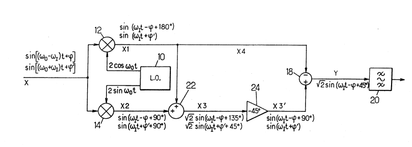
Figure 1 shows a conventional arrangement of an
image frequency rejection device. A local oscillator 10
delivers two quadrature waves at the transposition frequency
fo=~o/2~, which are each mixed with the input signal X by
2 1 92039
respective mixers 12, 14. With regard to the intermediate
frequency fI=~I/2~, the radio signal X possesses two
components to be considered, one written sin[(~0-~I)t+~] and
the other written sin[(~0+~I)t+~']. It is assumed here that
the desired comml~n;cation frequency fC is (~o-~I)/2~ and
that the frequency (~0+~I)/2~ is the undesirable image
frequency. The modulated phase which it is sought to extract
is then the phase ~. The output signal Xl from the mixer 12,
resulting from the mixing of the radio signal X with the
wave 2cos~0t possesses two components at the intermediate
frequency fI: one having the phase -~+180 and the other
having the phase ~'. The output signal X2 from the mixer 14,
resulting from the mixing of the radio signal X with the
wave 2sin~0t which has a phase lag of 90 with respect to
the wave 2cos~0t, likewise possesses two components at the
intermediate frequency: one having the phase -~+90 and the
other having the phase ~'+90. A phase-shifter filter 16
applies a 90 phase lag at the intermediate frequency to the
signal X2 so as to produce a signal X2' having, at the
intermediate frequency, a component of phase -~ and a
component of phase ~'. A subtractor 18 deducts the signal Xl
from this phase-shifted signal X2'. The undesirable phase ~
is thus eliminated from the output signal Y from the
subtractor 18. Only the desired phase ~ remains (bearing a
minus sign in this particular case). The output signal Y is
applied to a band-pass filter 20 which lets through the
components with frequency close to the intermediate
~ ~ 2 1 92039
frequency fI so as to extract the desired phase.
The major drawback of the device represented in
Figure 1 is the need for a 90 phase-shifter requiring two
poles and generally having to be embodied in the form of
discrete components. Furthermore, the paths followed by the
two signals combined by the subtractor 18 are not identical,
this affecting the effectiveness of the rejection.
In order to reduce the impact of these problems, it
has been proposed to replace the 90 phase-shifter with two
+45 phase-shifters. Figure 2 shows such an arrangement. The
phase-shifter 15 applies a 45 phase lead to the signal Xl
so as to produce a signal Xl" having, at the intermediate
frequency, a component of phase -~+225 and a component of
phase ~'+45. The phase-shifter 17 applies a 45 phase lag
to the signal X2 to produce a signal X2" having, at the
intermediate frequency, a component of phase -~+45 and a
component of phase ~'+45. The output signal Y=X2n-Xl" from
the subtractor 18 then possesses at the intermediate
frequency a single component of phase -~+45, that is to say
containing the useful information. It is noted that the
amplitude of this signal Y is smaller than that obtained
with the layout of Figure 1, given the ~ attenuation
afforded by the +45 phase-shifters 15, 17.
The device of Figure 2 improves on that of Figure 1,
especially in that it can be embodied in the form of an
integrated circuit. However, it is not free of drawbacks. In
particular, the construction of the two RC networks making
``- 21 92039
up the phase-shifter filters 15, 17 is tricky. The matching
of these two networks is tricky and requires compensations.
In general, one of the capacitances is not floating and it
is therefore necessary to take account of its stray
capacitance, for example by placing follower stages with low
output impedance upstream of the phase-shifter filters. To
obtain sufficiently effective rejection, the phase-shifter
networks usually have to be tuned by means of digital/analog
converters. Furthermore, the device has constantly to adapt
to changes in the environment (temperature, supply voltage,
etc.) so as to optimize image rejection.
An object of the present invention is to propose a
simplified structure for a mixer device with image frequency
rejection which can be embodied entirely in the form of an
integrated circuit.
The invention thus proposes a mixer device with
image frequency rejection, comprising mixing means for form-
ing a first signal by mixing an input radio signal with a
first wave of frequency fO delivered by a local oscillator
and a second signal by mixing the input radio signal with a
second wave of frequency fO delivered by the local oscilla-
tor and having a phase lag of 90 with respect to said first
wave, and means of algebraic summation of third and fourth
mutually phase-shifted signals obtained from said first and
second signals, in order to produce an output signal
possessing, at the intermediate frequency fI, a phase repre-
sentative of the phase possessed by the input radio signal
21 92039
~_ 5
at a commlln;cation frequency fc of the form fO-fI or fO+fI,
with rejection of the phase which the input radio signal may
possess at the image frequency 2fo-fC. According to the
invention, the device further comprises phase-shifter means
producing said third signal by filtering an algebraic sum of
the first and second signals with a transfer function A(f),
and means for producing said fourth signal by applying to
one of said first and second signals a transfer function
B(f) such that, at the intermediate frequency fI, the ratio
A(fI)/B(fI) has modulus 1/~ and argument +45 or +135.
The "algebraic sum" of two signals is understood
here to mean the sum or the difference of the two signals in
question.
The invention will be better understood on reading
the following description of preferred but non-limiting em-
bodiments, with reference to the appended drawings in which:
-Figures 1 and 2 are schematic layouts of mixer
devices with image frequency rejection of the prior art;
-Figures 3 to 10 are schematic layouts of eight
mixer devices according to the invention;
-Figure 11 is a basic layout of a device of the type
shown in Figure 3;
-Figure 12 is a phase diagram illustrating the
operation of the device of Figure 11;
-Figure 13 is a detailed layout of a device
according to Figure 7; and
-Figure 14 is a layout of a slaving circuit which
21 92039
can be used with a device according to Figure 13.
In Figures 3 to 10 the same numerical references as
in Figures 1 and 2 have been used to denote identical ele-
ments, especially the local oscillator 10 and the mixers 12,
14. To facilitate comparison with Figures 1 and 2, the case
is considered, in respect of Figures 3 to 10, in which the
transfer function referred to above as B(f) is equal to 1.
In the device represented in Figure 3, an adder 22
produces the sum X3 of the first signal Xl delivered by the
mixer 12 and of the second signal X2 delivered by the mixer
14. The signal X3 has a gain of ~ at the intermediate
frequency, given that it corresponds to a sum of two
quadrature vectors. At the intermediate frequency fI, the
signal X3 possesses a phase of -~+135 and a phase of
~'+45. A phase-shifter filter 24 applies a phase-shift to
the signal X3 to produce a signal X3'. This phase-shift
corresponds to a 45 phase lag at the intermediate frequency
fI, so that the signal X3' possesses, at the intermediate
frequency fI, a phase of -~+90 and a phase of ~'. The
attenuation introduced by the phase-shifter filter 24 at the
intermediate frequency compensates for the gain of ~ of the
signal X3. The subtractor 18 effects the difference between
the signal X3' and a signal X4=B(f).Xl=Xl. In this
difference Y, the undesirable phase ~' has been eliminated.
There remains, at the intermediate frequency fI, only the
phase -~+45, with a gain of ~, given that the subtractor
18 effects a sum of two quadrature signals sin(~It-~) and
21 92039
_
sin(~It-~+90). The output signal Y from the mixer device
can next be applied to the band-pass filter 20 for
subsequent processing operations.
In the device represented in Figure 4, the adder 22
is replaced by a subtractor 22a producing the difference
X3=X2-X1, the phase-shifter filter 24a introduces a +45
phase lead at the intermediate frequency so as to produce
the signal X3' from the difference signal X3, and the
subtractor 18 is replaced by an adder 18a producing
10Y=X3'+X4=X3'+X1. In this case, the signal X3 possesses, at
the intermediate frequency, phases -~+45 and ~'+135, so
that the phase-shifted signal X3' possesses, at the interme-
diate frequency, the phases -~+90 and ~'+180. As a conse-
quence, the undesirable phase ~' is eliminated from the out-
15put signal Y, which, at the intermediate frequency, has only
the phase -~+135 representative of the phase ~ possessed by
the input signal X at the communication frequency fc=fo-fI-
In the device schematized in Figure 5, the adder 22b
produces the signal X3=Xl+X2 possessing, at the intermediate
20frequency, the phases -~+135 and ~'+45. The phase-shifter
filter 24b applies a +45 phase-shift to the signal X3 to
produce a signal X3' having, at the intermediate frequency,
the phases -~+180 and ~'+90. The subtractor 18b produces
an output signal Y=X3'-X4=X3'-X2 possessing only the phase
25-~-135 at the intermediate frequency.
In the device represented in Figure 6, the
subtractor 22c produces the signal X3=X2-X1 possessing, at
` `i 21 9203q
the intermediate frequency, the phases -~+45 and ~'+135.
The phase-shifter 24c applies a -45 phase-shift to the
signal X3 at the intermediate frequency to produce a signal
X3' having, at the intermediate frequency, the phases -~ and
~'+90. The subtractor 18c produces an output signal
Y=X3'-X4=X3'-X2 possessing only the phase -~-45 at the
intermediate frequency.
In the explanations given above with reference to
Figures 3 to 6, the "first signal" X1 was obtained by mixing
with the input radio signal X a wave 2cos~0t having a phase
lead of 90 with respect to the wave 2sin~0t mixed with the
input radio signal to form the "second signal" X2. This
makes it possible to extract at the intermediate frequency
a phase representative of the phase ~ possessed by the input
radio signal at a comml~n;cation frequency fC=fO~fI while
rejecting the image frequency 2fo-fC=fo+fI.
In the case in which the commlln;cation frequency fC
is of the form fO+fI, it is the phase ~' which it is sought
to extract at the intermediate frequency, while eliminating
the image frequency 2fo-fC=fo-fI. In this case, it is
appropriate to permute the roles of the signals X1 and X2.
Figures 7 to 10 are thus layouts of devices
respectively similar to those of Figures 3 to 6, in which
the roles of the signals X1 and X2 have been permuted in the
combinations performed in order to deliver the output signal
Y, and therefore appropriate in respect of a com.munication
frequency fC=fO+fI with rejection of the image frequency
21 9203q
~ 9
fO-fI -
In the device of Figure 7, the phase-shifter 24d
retards by 45 the phase of the signal X3=Xl+X2 produced by
the adder 22d. The subtractor 18d subtracts the signal X4=X2
from the output X3' from the phase-shifter 24d so that the
output signal Y has only the phase ~'-45 at the
intermediate frequency.
In the device of Figure 8, the phase-shifter 24e
advances by 45 the phase of the signal X3=Xl-X2 produced by
the subtractor 22e. The adder 18e adds the signal X4=X2 to
the output X3' from the phase-shifter 24e so that the output
signal Y has only the phase ~'+45 at the intermediate
frequency.
In the device of Figure 9, the phase-shifter 24f
advances by 45 the phase of the signal X3=Xl+X2 produced by
the adder 22f. The subtractor 18f subtracts the signal X4=Xl
from the output X3' from the phase-shifter 24f so that the
output signal Y has only the phase ~'+135 at the
intermediate frequency.
In the device of Figure 10, the phase-shifter 24g
retards by 45 the phase of the signal X3=Xl-X2 produced by
the adder 22g. The subtractor 18g subtracts the signal X4=Xl
from the output X3' from the phase-shifter 24g so that the
output signal Y has only the phase ~'-135 at the
intermediate frequency.
In the general case, when the communication
frequency fC is of the form fO-fI, the combination applied
21 9203q
-
to the signals Xl and X2 to produce the output signal Y is
such that Y is the real part of a complex signal
proportional to (Xl+X2)e j~t4/~-Xl (Figure 3), to
(X2-Xl)ej~/4/r~+Xl (Figure 4), to (Xl+X2)ei~/4/~2-X2 (Figure
5), or to (X2-Xl)e i~/4/~-x2 (Figure 6). Figures 3 to 6
correspond to the case in which the constant of
proportionality is equal to 1. In the general case, this
constant of proportionality can be any complex number B(fI).
When the csmmlln;cation frequency fC is of the form
fO+fI, the combination applied to the signals Xl and X2 to
produce the output signal Y is such that Y is the real part
of a complex signal proportional to (Xl+X2)e~i~/4/~-X2
(Figure 7), to (Xl-X2)ei~/4/ ~ +X2 (Figure 8), to
(Xl+X2)ei~/4/~-Xl (Figure 9) or to (Xl-X2)e i~/4/~-Xl
(Figure 10). Figures 7 to 10 correspond to the case in which
the constant of proportionality is equal to 1. In the
general case, this constant of proportionality can be any
complex number B(fI).
As e3i~/4=-e-j~/4 and e~3i~/4=_ei~/4, the aforesaid
phase-shifts, obtained via +45 phase-shifter filters at the
intermediate frequency in the layouts of Figures 3 to 10,
could also be obtained via +135 phase-shifter filters at
the intermediate frequency, through a corresponding
modification of the signs in the algebraic sums.
Figure 11 shows a basic layout of an embodiment of
a mixer device according to Figure 3, in which the first and
second signals Xl, X2 are produced in the form of current
2192039
11
signals. In Figure 11, the mixers 12, 14 are schematized by
current generators yielding currents I01 and I90 of like
amplitude I0 and corresponding respectively to the signals
Xl and X2. There is provision for a duplication of the
generator 12. Thus, the generator 12' yields a current I02
equal to the current I01. The sum Il=IOl+I90 of the currents
produced by the generators 12, 14, which represents the
signal X3, is applied to a first common terminal of a
resistor 30 and a capacitor 32 making up the phase-shifter
filter 24. The resistor 30 and the capacitor 32 are mounted
in parallel between this first terminal and a second
terminal taken to a reference potential, for example a
positive potential or, as represented, the ground potential.
The ohmic value R of the resistor 30 and the capacitance C
of the capacitor 32 are adjusted so as to satisfy the
relation RC~I=l, so that the RC filter 24 introduces a 45
phase lag at the intermediate frequency fI=~I/2~ between the
voltage Vl at the first terminal, which represents the
signal X3', and the current Il injected by the generators
12, 14 at this first terminal. In complex notation, we have
Vl=R.Il/(l+j) at the intermediate frequency, i.e.
X3'=R.X3.e~i~/4/~. The device further includes a resistor
34 with the same ohmic value R as the first resistor 30,
connected between the second terminal at the reference
potential and a third terminal at which the current I02
produced by the generator 12' is injected. The voltage
V2=R.I02 present at this third terminal, which represents
2 1 92039
the signal X4, is therefore in phase with the signal Xl
which the current I02 represents: X4=R.Xl. The subtractor 18
then produces the signal Y=R[ (xl+x2)e-i~/4/r-xl] by
differencing the voltage signals Vl and V2. The transfer
functions A(f) and B(f) are in this case impedances such
that B(f)=R and A(fI)=R.e~i~/4/~.
If, at the intermediate frequency fI, the current
I90 has a phase lead of 90 with respect to the currents I01
and I02, the current Il+=IOl+I90=(l+j)IOl exhibits a +45
phase-shift with respect to the currents I01 and I02 (Figure
12). The voltage Vl+=R. Il+/(l+j)=R.IOl which results from
this then has the same amplitude and the same phase as the
voltage V2, so that these two voltages are cancelled out on
output from the subtractor 18. This situation is that of the
components sin(~It+~') and sin(~It+~'+90) of the signals Xl
and X2 (Figure 3).
If, at the intermediate frequency fI, the current
I90 has a phase lag of 90 with respect to the currents I01
and I02, the sum Il_=IOl+I90=(1-j)IOl exhibits a -45 phase-
shift with respect to the currents I01 and I02. The voltage
Vl_=R.Il_/(l+j)=-j.IOl which results from this then has the
same amplitude as the voltage V2, with a phase-shift of -90
(Figure 12). The output signal Y=Vl_-V2 is then non-zero.
In complex notation, Y=R.(-l-j).IOl. This situation is that
of the components sin(~It-~+180) and sin(~It-~+90) of the
signals Xl and X2 (Figure 3).
The basic layout of Figure 11, depicted in the case
1 . ~ 21 92039
of a mixer device according to Claim 3, is manifestly
transposable to mixer devices according to Figures 4 to 10.
It is therefore seen that a device according to the
invention can be embodied in a particularly simple manner by
using a phase-shifter filter consisting of a simple parallel
RC network without floating capacitance, it being possible
for the algebraic sum schematized by the summators 22, 22a-g
in Figures 3 to 10 to be embodied simply by injection of two
currents at a terminal of this RC network.
Figure 13 shows an embodiment of a mixer device
according to Figure 7, in which the signals are differential
signals, the communication frequency being of the form
fC=fO+fI (for example fo=30.6 MHz, fI=10.7 MHz and
fc=41.3 MHz). The mixers 12,14 consist of Gilbert cells with
npn transistors.
The cell 12 comprises a first stage of two npn
transistors 42, 52 whose emitters are linked by a
linearizing resistor 46 whose value could be zero, the base
of the transistor 42 receiving the input radio signal X and
the base of the transistor 52 receiving the additive inverse
X of this signal X. The drain of an NMOS transistor 47 is
linked to the emitter of the npn transistor 52. This
transistor 47 is arranged so as to yield a constant current,
for example of 60 ~A. To do this, its source is grounded,
and its gate is taken to a fixed voltage VF present on the
common drain-gate connection of another NMOS transistor 50
biased to saturation, with its source grounded. A current
; 2 ~ 92039
14
generator 51 injects a stable current so as to bias the
transistor 50. The cell 12 comprises a second stage of four
npn transistors 62, 72, 82, 92. The emitters of the
transistors 62, 72 are linked to the collector of the
transistor 42, whilst the emitters of the transistors 82, 92
are linked to the collector of the transistor 52. The bases
of the transistors 62 and 92 receive a sinusoidal voltage
signal C at the frequency fO arising from the local
oscillator (wave cos~Ot), whilst the bases of the
transistors 72 and 82 receive a sinusoidal voltage signal C
at the frequency fO arising from the local oscillator 10 and
corresponding to the signal C phase-shifted by 180. The
collectors of the transistors 62 and 82 are linked together,
as are those of the transistors 72 and 92.
With this arrangement, the Gilbert cell 12 yields
the mixed signal Xl in the form of the difference between
the current il arising from the collectors of the
transistors 62, 82 and the current i2 arising from the
collectors of the transistors 72, 92: Xl=il-i2. This
differential signal Xl is proportional to X.cos~Ot.
The cell 14 has a structure similar to that of the
cell 12, with a first stage of two npn transistors 44, 54
whose emitters are linked by a linearizing resistor 48, the
base of the transistor 44 receiving the input radio signal
X and the base of the transistor 54 receiving the signal X.
The drain of an NMOS transistor 49 identical to the
transistor 47 is linked to the emitter of the npn transistor
21 q2039
44. This transistor 49 has its source grounded, and its gate
receives the same constant voltage VF as that of the
transistor 47. In order to balance the cells, the collectors
of the transistors 42, 44 are linked together, as are the
collectors of the transistors 52, 54. The cell 14 comprises
a second stage of four npn transistors 64, 74, 84, 94. The
emitters of the transistors 64, 74 are linked to the
collector of the transistor 54, whilst the emitters of the
transistors 84, 94 are linked to the collector of the
transistor 44. The bases of the transistors 64 and 94
receive a sinusoidal voltage signal S at the frequency fO
arising from the local oscillator 10 and corresponding to
the signal C with a 90 phase lag (wave sin~Ot~, whilst the
bases of the transistors 74 and 84 receive a sinusoidal
voltage signal S at the frequency fO and corresponding to
the signal S phase-shifted by 180. The collectors of the
transistors 64 and 84 are linked together, as are those of
the transistors 74 and 94.
With this arrangement, the Gilbert cell 14 yields
the mixed signal X2 in the form of the difference between
the current i3 arising from the collectors of the
transistors 74, 94 and the current i4 arising from the
collectors of the transistors 64, 84: X2=i3-i4. This
differential signal X2 is proportional to X.sin~Ot, the
constant of proportionality being the same as that of the
differential signal Xl delivered by the cell 12.
For the biasing of the transistors 42, 52, 44, 54,
~ 21 92039
.
16
the voltage signals X and X are superimposed on a DC voltage
BS before being forwarded to the bases of the transistors
42, 44 and 52, 54. This voltage BS is produced by two npn
transistors in series 56, 57 mounted as a diode. The tran-
sistor 56 has its collector and its base linked to a supplyterminal at a positive voltage VA. The transistor 57 has its
collector and its base linked to the emitter of the transis-
tor 56, and its emitter linked to the drain of an NMOS
transistor 58. The source of the transistor 58 is grounded
and its gate is at the voltage VF. The voltage BS, present
on the emitter of the transistor 57, is then BS=VA-2Vbe,
where Vbe is the base-emitter saturation voltage of the
transistors 56, 57. In order to bias the transistors of the
first stages of the Gilbert cells, the emitter of the tran-
sistor 57 is linked to the bases of the transistors 42, 44
and 52, 54 by way of respective biasing resistors 59 and 60.
In order to effect the addition schematized by the
adder 22d in Figure 7, the currents il and i3 are injected
at a common node 66, and the currents i2 and i4 are injected
at a common node 67. Thus, the signal X3 represented in
Figure 7 is the differential current signal corresponding to
the difference between the current i5=il+i3 issuing from the
node 66 and the current i6=i2+i4 issuing from the node 67:
X3=i5-i6.
In order to yield the second version of the signal
X2, which version will be combined with the signal phase-
shifted by 45, the second stage of the Gilbert cell 14 is
' ~
21 92039
17
duplicated. There is thus provided a stage 14' consisting of
four npn transistors 65, 75, 85, 95 connected in the same
way as the transistors 64, 74, 84, 94 of the second stage of
the cell 14. A second version of the currents i3 and i4 is
thus available on the common connection of the collectors of
the transistors 75, 95 and on the common connection of
collectors of the transistors 65, 85.
For reasons of symmetry, a duplication of the second
stage of the Gilbert cell 12 is also provided for. The stage
12' thus consists of four npn transistors 63, 73, 83, 93
connected in the same way as the transistors 62, 72, 82, 92
of the second stage of the cell 12. A second version of the
currents il and i2 is thus available on the common connec-
tion of the collectors of the transistors 63, 83 and on the
common connection of collectors of the transistors 73, 93.
The mixer device of Figure 13 further comprises four
PMOS transistors 68, 69, 70, 71 biased so as to operate in
their ohmic region, and four npn transistors 78, 79, 80, 81
in a cascode configuration. The sources of the PMOS
transistors 68-71 and the bases of the npn transistors 78-81
are each at the positive supply voltage VA. The drains of
the transistors 68, 69, 70, 71 are respectively linked to
the collectors of the transistors 78, 79, 80, 81. The
emitter of the transistor 78 receives the current i5 issuing
from the node 66. The emitter of the transistor 79 receives
the current i3 issuing from the collectors of the
transistors 75, 95 of stage 14'. The emitter of the
~, t, 2 1 92039
18
transistor 80 receives the current i4 issuing from the
collectors of the transistors 65, 85 of stage 14'. The
emitter of the transistor 81 receives the current i6 issuing
from the node 67. The emitters of the transistors 78, 79,
80, 81 are moreover linked to the terminal at which the
supply voltage VA is present, by way of respective filtering
capacitors 88, 89, 90, 91.
The resistors of the channels of the transistors 68,
71 play a role similar to that of the resistor 30 of Figure
11, whilst the channels of the transistors 69, 70 play a
role similar to that of the resistor 34 in Figure 11. The
resistance values of these channels of the transistors 68-71
are fixed by an adjustment voltage VK forwarded to the gates
of these transistors. The channels of the transistors 68, 71
are connected in parallel with respective capacitors 98, 101
playing the role of the capacitor 32 of Figure 11.
The voltages on the drains of the PMOS transistors
71, 68, 70, 69 are denoted Al, A2, Bl, B2 respectively. The
differential voltage Al-A2 corresponds to the phase-shifted
signal denoted X3' in Figure 7, and the differential voltage
Bl-B2 corresponds to the signal denoted X4 in Figure 7. The
means corresponding to the subtractor 18d of Figure 7 are
arranged so as to yield the output signal Y given by
Y=Al-A2-Bl+B2. In the example represented in Figure 13,
these means comprise two differential amplifiers 102, 103
followed by an adder amplifier 104 delivering the signal Y.
The differential amplifier 102 has a positive input
21 92039
19
receiving the voltage Al and a negative input receiving the
voltage Bl, whilst the differential amplifier 103 has a
positive input receiving the voltage B2 and a negative input
receiving the voltage A2. The outputs of the two
differential amplifiers 102, 103 are linked to the inputs of
the adder amplifier 104.
With the circuit represented in Figure 13, we have
Al(f)=-ZA(f).i6(f), A2(f)=-ZA(f).i5(f), Bl(f)=-ZB(f).i4(f),
and B2(f)=-ZB(f).i3(f), where Al(f), A2(f), Bl(f), B2(f),
and i3(f) to i6(f) denote the Fourier components at the
frequency f of the signals Al, A2, Bl, B2 and i3 to i6, and
ZA(f)~ ZB(f) denote the complex impedances:
Ro
ZA( ) 1+2~jRo (co+cp) f
Rl
Z~(f) 1+2~jRlCpf
Ro denoting the resistance of the channels of the PMOS tran-
sistors 68, 71, Rl denoting the resistance of the channels
of the PMOS transistors 69, 70, C0 denoting the capacitance
of the capacitors 98, 101, and Cp denoting a stray capaci-
tance due essentially to the collector of each of the npn
transistors 78-81 (Cp is a capacitance between a collector
and the reference terminal at the voltage VA). One of the
reasons why the stage of cascoded transistors 78-81 is used
t, 21 q2039
is that it makes it possible to reduce these stray capaci-
tances: each input of the differential amplifiers 102, 103
n sees~ a single stray capacitance Cp corresponding to the
collector of the transistor 78-81 to which it is linked,
instead of several if the inputs of the differential ampli-
fiers were linked directly to the collectors of the transis-
tors of the Gilbert cells. The value of the stray capaci-
tance Cp can be known with reasonable accuracy by means of
simulations of the electronic behaviour of the integrated
circuit (it is typically of the order of 10% of C0).
Since X3l(f)=Al(f)-A2(f)=zA(f).[i5(f)-i6(f)]
=ZA(f).X3(f) and X4(f)=Bl(f)-B2(f)=zB(f).[i3(f)-i4(f)]
=ZB(f).X2(f),the complex impedances ZA(f) and ZB(f) are the
transfer functions A(f) and B(f) between the differential
signals X3 and X3' and between the differential signals X2
and X4.
The values of the resistances Ro and Rl are chosen
as follows:
2 ~ fI ( Co ~ Cp)
Rl = 2 fl C = Ro(l- CP)
so that at the intermediate frequency fI, the transfer
functions A(f) and B(f) are such that A(fI)/B(fI)=(l-j)/2
=e~i~/4/~ with B(fI)=1/[2~fI(Co+jCp)]. Consequently, the
output voltage Y has, at the frequency fI, a component Y(fI)
2 1 9203~
21
proportional to
Al(fI)-A2(fI)-Bl(fI)+B2(fI)
= B(fI).[X3(fI).e j~/4/ ~ - X2(fI)]
With the gates of the transistors 68-71 being fed
with the same signal VK, the different values of the
resistances Ro and R1 indicated above are obtained by
providing, for the PMOS transistors 68, 71, a channel of
equal length but of smaller width than the channel of the
PMOS transistors 69, 70.
The circuit represented in Figure 13 further
includes means for balancing the DC voltages on the inputs
of the differential amplifiers 102, 103. There are thus
provided two NMOS transistors 108, 109 having their sources
connected to ground, their gates connected to the voltage VF
and their drains linked respectively to the emitters of the
npn transistors 79, 80. These transistors inject a constant
current i0 into the emitters of the transistors 79, 80 so as
to compensate for the fact that the resistance R1 of the
channels of the PMOS transistors 69, 70 is smaller than the
resistance of the channels of the PMOS transistors 68, 71.
The capacitors 88-91 have substantially smaller
capacitances than those of the capacitors 98 and 101. These
capacitors 88-91 serve, with the input impedances (emitters)
of the npn transistors 78, 81, to filter out high-frequency
harmonics from the mixed signals so as not to disturb the
inputs of the differential amplifiers 102, 103. The
capacitance of the capacitors 89, 90 is a little larger than
21 92039
~ 22
that of the capacitors 88, 91, so as to take into account
the fact that the input impedance of the transistors 79, 80
is smaller than that of the transistors 78, 81.
The circuit moreover comprises a stage 110 of eight
npn transistors 111-118 whose emitters are collectively
linked to the collector of another npn transistor 120. The
base of the transistor 120 receives the DC bias voltage BS
and its emitter is linked to the drain of an NMOS transistor
121 with identical characteristics to those of the
transistors 47, 49, whose source is grounded and whose gate
receives the voltage VF. The bases of the transistors 111,
114 receive the wave C. The bases of the transistors 112,
113 receive the wave C. The bases of the transistors 115,
118 receive the wave S. The bases of the transistors 116,
117 receive the wave S. The collectors of the transistors
111, 113 are linked to the emitter of the npn transistor 80,
whilst the collectors of the transistors 112, 114 are linked
to the emitter of the npn transistor 79. This compensates
for the fact that the emitters of the transistors 79, 80 are
each linked to only two transistors of the Gilbert cells 12,
12', 14, 14' whereas the emitters of the transistors 78, 81
are linked to four transistors of the Gilbert cells 12, 12',
14, 14'. Two other npn transistors in cascode configuration
76, 77, having their collectors and their bases at the
positive supply voltage VA, have their emitters linked to
the collectors of the transistors 63, 73, 83, 93, 115, 116,
117, 118 so as to balance the circuit.
21 92039
-
23
The high-frequency filtering carried out by the
capacitors 88-91 and the injection of the currents i0 and of
the currents arising from the stage 110 have virtually no
influence near the intermediate frequency fI, so that they
do not affect the complex impedances ZA and ZB at the
frequency fI.
It is noted that if the waves S and C (and S and C)
are permuted in the layout of Figure 13, this being readily
realizable by means of switches placed between the local
oscillator and the mixer device, then the signal X1 is
represented by i3-i4 and the signal X2 by il-i2. With such
a permutation, the device of Figure 13 becomes suitable for
a communication frequency of the form fC=f0~fI (cf. Figure
3).
The fact of using variable resistors such as the
channels of the MOS transistors 68-71 allows slaving of
these resistors so as to compensate for any variations due
to the manufacturing process or to outside parameters such
as the temperature or the supply voltages.
Figure 14 shows a circuit 125 for slaving the
voltage VK for adjusting the values of the resistances Ro
and R1 of the channels of the PMOS transistors 68-71. This
circuit 125 comprises four PMOS transistors 130-133 having
their sources at the supply voltage VA, and their gates at
the voltage VK delivered by a variable voltage generator
135. The transistors 130 and 131, which are each mounted in
parallel with a respective capacitor 136, 137, are identical
21 92039
-
24
to the PMOS transistors 68, 71 of resistance Ro, and the
transistors 132 and 133 are identical to the PMOS
transistors 69, 70 of resistance Rl=Ro(l-Cp/Co). The drains
of the transistors 130-133 are each linked to the output of
a respective transconductance amplifier 140-143. The drains
of the transistors 130 and 132 are furthermore linked to the
inputs of the transconductance amplifiers 141 and 143
respectively. The slaving circuit 125 thus comprises two
cascaded RC filters 138, 139, the first made up of the
transconductance amplifier 140, the transistor 130 and the
capacitor 136, and the second made up of the
transconductance amplifier 141, the transistor 131 and the
capacitor 137, and on the other hand two cascaded all-pass
cells 148, 149, the first made up of the transconductance
amplifier 142 and the transistor 132, and the second made up
of the transconductance amplifier 143 and the transistor
133. The inputs of the transconductance amplifiers 140 and
142 receive a sinusoidal wave W of fixed frequency fl close
to the intermediate frequency fI. The drains of the
transistors 131 and 133 are furthermore linked to the two
inputs of a multiplier 145. The output of the multiplier 145
is linked to the input of a low-pass filter 146 having a
cutoff frequency substantially below fl. The output signal
from the filter 146 is forwarded to the generator 135 in
order to fix the value of the voltage VK. The
transconductance amplifiers 140-143 can consist of Gilbert
cells similar to the cells 12, 14 with a stage of npn
2 1 92039
transistors mounted in cascode in similar manner to the
transistors 78-81 so as to exhibit a stray capacitance Cp of
the same order on the collectors of these npn transistors.
The capacitors 136 and 137 are sized so that their
capacitance is C'o=Co.fI/fl. Thus, the cascaded RC filters
138 and 139 each introduce at the frequency fl a phase-shift
of ~+~/4 when the voltage VK is at the proper value (that
for which 2~fIRo(Co-Cp)=1 and 2~fIRlCo=l), ~ representing
the phase-shift introduced by the cells 148, 149. The wave
W being of the form sin2~flt, the two inputs of the
multiplier 145 are in quadrature when the voltage VK has the
proper value, so that the output from the multiplier is at
the frequency 2fl and control of the variable generator 135
is not modified owing to the low-pass filtering. If, on the
other hand, the voltage VK deviates from the proper value,
the multiplier 145 delivers a DC component which, integrated
by the filter 146, restores the voltage VK to the proper
value.
The frequency fl of operation of the slaving circuit
125 would ideally be equal to the intermediate frequency fI.
However, since a sinusoidal wave is not necessarily
available at the intermediate frequency, a readily available
frequency fl is chosen which is close to fI, by taking into
account the difference in the capacitance C'o=CofI/fl. In
the case of an intermediate frequency of 10.7 MHz, it is for
example possible to use a frequency fl of 11.15 MHz if a
quartz resonating at this frequency is available.
21 q2039
26
In the case of a mixer device according to Figure
11, that is to say when the stray capacitances may be
regarded as negligible, there is no difference between the
ohmic values of the resistors 30 and 34 (Ro=Rl=R), and a
slaving circuit of the same kind as that of Figure 14 can be
used to slave the value of R when the identical resistors
30, 34 are variable resistors. The slaving then ensures that
2~RCfI=l independently of outside fluctuations.