Note: Descriptions are shown in the official language in which they were submitted.
WO 95134119 PCTIUS95106875
s. , .
STRUCTURE AND METHOD FOR PERFORMING ACTIVE
INJECTION MODE FILTERING ON
AN AC POWER SYSTEM
Field of the Invention
The present invention generally relates to an
apparatus and method for injecting non-fundamental
frequency current-components onto an AC power line, and
in particular to a shunt-mode active injection mode
(AIM) filter which provides the non-fundamental
frequency currents drawn by a non-linear load to
prevent those non-fundamental frequency currents from
flowing to the AC power source.
Background of the Invention
In conventional alternating current power systems,
power is transmitted from an AC power source, through a
network of power lines and through transformers to
supply either three-phase or single-phase loads. These
loads typically consist of both linear and non-linear
elements. Power is provided on the power system at a
fundamental frequency, fo, typically 60 Hz. However,
certain non-linear loads also draw undesired currents
having frequencies other than the fundamental line
frequency (e. g., harmonics fz=2fp, f3=3fo, etc.). These
undesired current components are referred to as non-
fundamental frequency currents.
Non-linear loads, such as AC-DC rectifier power
supplies, draw non-fundamental frequency currents.
Typically, these non-fundamental frequency currents are
supplied from the AC power source to the load along
-1-
W0 95134119 PCTIUS95106875
~~ ~ 192189
power lines and through transformers. Excessive non-
fundamental frequency currents can produce serious
voltage distortion on power lines when they interact
with the source impedances of the power system
(including the impedances of the AC power source and
the power lines). Excessive non-fundamental frequency
currents and their associated voltages can also cause
interference, overheating of power lines and
transformers and malfunctioning of other equipment
connected to-the upstream AC power system.
An AIM filter is an electronic power conversion
device that is connected in shunt across a power line
to compensate for non-fundamental frequency currents
drawn by a load. The AIM filter is typically located
near the load which draws the undesirable non-
fundamental frequency currents. In general, an AIM
filter senses the non-fundamental frequency currents
being drawn by the load, attempts to generate currents
which match these non-fundamental frequency currents,
and injects these matching non-fundamental frequency
currents back onto the power line. In this manner, the
AIM filter provides the non-fundamental frequency
current components required by the load so that these
currents do not flow from the AC power source to the
point where the AIM filter connects to the power line.
An AIM device can also be used to test the
response of an AC power source to nonlinear loading or
the imperviousness of a load (e. g., electronic
equipment) to poor quality electrical power. In such
an application, the AIM device does not sense the
current present on the power line, but instead
generates predetermined non-fundamental frequency
current components. These current components are then
injected onto a power line that might not otherwise
experience non-fundamental frequency currents. The
-2-
W095/34119 ., _ . PCT1US95/06875
response of the AC power source or the load is then
observed to determine how it will perform when exposed -
to such conditions.
. Fig. 1 is a single-line diagram of a prior art AIM
filter 17 connected to an AC power system. AC power
source 10 transmits a current of IS at a voltage of VLUrs
to load 12 on power line 11. Load 12 generally
includes a linear element 41 having impedance ZL and a
non-fundamental frequency current generator 42, which
to draw currents I~ and IH, respectively.
Current transducer 15 is coupled to power line il
to sense the current IL drawn by load 12. Current
transducer 15 provides a signal V,a, which is
proportional to current IL, to harmonic current detector
16. Harmonic current detector 16 filters the
fundamental frequency current component of signal V,o to
produce a voltage signal V" proportional to the non-
fundamental frequency current components being drawn by
load 12, i.e. the non-fundamental frequency current
components of both I~ and IH.
Voltage signal V" is transmitted through summing
node 18, amplifier 19 and summing node 20 of
transconductance amplifier 24. In response,
transconductance amplifier 24 generates a current
output I1 which is proportional to input voltage signal
V". The gain of transconductance amplifier 24 is
controlled so that the current I1 produced by
transconductance amplifier 24 is equal to the non-
fundamental frequency current components of the load
current IL.
Transconductance amplifier 24 typically includes a
pulse width modulator circuit 23, a high-speed
switching circuit 26, an output inductor 30 and a
current transducer 28. Transducer 28 provides a
current feedback signal V,2 to summing node 18 to make
the amplifier a transconductance amplifier, i.e. an
-3-
. , ~ . . ,;,~,
M 2853 PCL;9309 ..o3,~az~~, - -. -.... - PCT/US 95.-/06 8 75
~ 219218 9 IPEA/US a s sEp ~sss
amplifier that produces an output current in response
to an input voltage signal. Inductor 30 and passive
S filter-32 remove high frequency switching current
components introduced by pulse width modulator circuit
23 and transistor switching circuit 26. _
Voltage sensor 22 provides a line voltage feed _
forward signal inside the current control feedback loop
that reduces the necessary gain of the current control
faedback loop, increasing the stability of that loop.
The output current I1 of transconductance amplifier
24 produces all of the non-fundamental frequency
current components of load current IL, including IH and
IS the non-fundamental frequency components of IZL. Thus,
the effect of current I" is to isolate the non-
fundamental frequency components of linear element 41
from the AC power line and unload any non-fundamental
frequency voltage components of V;,Ij,g. This unloading
can result in instability of the power system and
increased non-fundamental frequency voltages on the
power system.
For transconductance amplifier 24 to produce the
desired flow of current on power line 11, the
transconductance amplifier 24 must be able to generate
-- an instantaneous voltage V1 equal to
VLIi,g(t) + L*dIl/dt
where VL=,,~(t) is the AC power line voltage, VLF, at
time t at node 13, L is the inductance of inductor 30 -
and dIl/dt is the derivative of output current I1 with
respect to time.
In AIM filter applications such as the one
described above, dIl/dt can be substantial, especially
in three-phase systems. For a typical non-linear
rectifier.type load, the waveform of load current IL
comprises alternating positive and negative rectangular
- 4 -
AMENDED SHEET
W O 95/34119
P~~S95106875
t. -, 9 8 9
, , :;, '; 2 j 21
current pulses with fast
rising and falling edges,
i.e.
a large dIl/dt. The voltage
that must be produced
across inductor 30 (L*dIl/dt)
to produce the fast
rising and falling edges
of the current pulses can
approach the peak value
of the line voltage VIE.
The
peak value of dIl/dt typically
occurs when the line
voltage V~ is between 50%
and 100% of its peak value.
Consequently, the required
voltage V1 which must be
generated at the output
of switching circuit 26
approaches twice the peak
voltage V~ of power line
11.
If the transistor switching
circuit 26 is not capable
of providing the required
voltage V1, transconductance
amplifier 24 will not be
able to produce the desired
output current I1.
Even at the lowest typical
voltages of VIE (e. g.
208 Volts AC line-to-line),
the peak output voltage
V1
of switching circuit 26
must be at least 600 V
to
provide the desired output
currents. The fast
switching devices needed
to generate high frequency
currents at voltages above
approximately 600 V are
eithernot available or expensive.
Furthermore, the
switching losses in the
switching circuit 26 increase
substantially as the output
voltage V1 increases,
thereby resulting in a loss
of efficiency within the
transconductance amplifier
24.
Guidelines presently being
discussed for harmonic
suppression of utility line
connected equipment and
adopted as specifications
for some new installations
place lower limits on the
allowable high frequency
harmonic currents than on
the allowable lower frequency
harmonic currents. (See,
e.g., IEEE Practices and
Requirements for Harmonic
Control in Electric Power
Systems, IEEE Standard 519-1992.)
It would therefore be desirable
to have an AIM
filter having a switching
stage capable of operating
at
a reduced voltage.
-5-
WO 95/34119 ~ i' ~ 2, ~ g 2 l 8 9 PCTIUS95106875
Summary of the Invention
In one embodiment of the present invention, an
active current injection device is used to generate and
inject fundamental and non-fundamental frequency
current components onto an AC power line. A current
pump control circuit receives an input signal which is
representative of the line voltage of the power line.
In response, the current pump control circuit generates
a control signal which is used to generate a current
l0 component at the fundamental frequency which lags the
line voltage by approximately 90 degrees. This
fundamental frequency current component is transmitted
through an impedance to the power line, thereby causing
a voltage drop at the fundamental frequency across the
impedance. This voltage drop is within a selected
range about the line voltage. In one-embodiment, this
selected range is equal to approximately 25 to
approximately 150 percent of the line voltage. In
another embodiment, this voltage drop is approximately
equal to the line voltage. The voltage dropped across
the impedance reduces the required operating voltage of
the active current injection device. In one
embodiment, the impedance is a capacitor and the
current generated in response to the current pump
control circuit advantageously provides current having
a leading power factor as seen by the power line.
In another embodiment of the present invention, a
damping control circuit receives an input signal which
is representative of the line voltage of the power
line. In response, the damping control circuit
generates an output signal having a first component
proportional to the line voltage and a second component
proportional to the rate of change of the line voltage.
This output signal is used to generate an electronic
load current component which is provided to the power
line. The electronic load current component loads the
-6-
W0 95134119 PCT/US95106875
2192189
non-fundamental frequency components of the line
voltage, thereby advantageously preventing both system
instability and possible increases in the non-
fundamental frequency voltages. System instability and
increased non-fundamental frequency voltages were
previously caused by the unloading of the non-
fundamental frequency voltages in prior art AIM
filters. In one embodiment, the electronic load
current component is selected to approximate the linear
element of a downstream load.
In yet another embodiment of the present
invention, a four-conductor adapter circuit is coupled
to an active current injection device to facilitate
operation in a four-conductor, three-phase system. The
four-conductor system includes three power conductors
and a neutral conductor. The four-conductor adapter ,
circuit receives inputs from the three power conductors
which are representative of the currents on these
conductors. In response, the four-conductor adapter
circuit creates a first signal proportional to the
current on one power conductor minus one third of the
current on the neutral conductor and a second signal
which is proportional to the current on another power
conductor minus one third of the current on the neutral
conductor. In one embodiment, the first and second
signals are provided to an AIM filter which generates a
first output current component responsive to the first
signal, a second output current component responsive to
the second signal and a third output current component
equal to the negative sum of the first and second
output current components. The effect of the four-
conductor adapter circuit is that the non-fundamental
frequency currents flowing from the AC power source on
the three power conductors are equal in phase and
amplitude and equal to one third of the non-fundamental
frequency current flowing to the AC power source on the
_7_
W095134119 4 , . ~r~ ~ ~ ~ ~ ~ PCTIUS95106875
neutral Line: -
Further advantages of the present invention will
become apparent in view of the following description
and drawings.
Rriaf TlPecrint;on of the Drawinq~ -... . .. . ...
Fig. 1 is a single-line diagram of a prior art AIM
filter connected to an AC power system;
Fig. 2 is a single-line diagram of an active
current injection device in accordance with one
embodiment of the present invention;
Fig. 3 is a three-phase circuit diagram of active
current injection device in accordance with one
embodiment of the present invention;
Fig. 4 is a circuit diagram of one embodiment of a
pulse width modulation control circuit;
Fig. 5 is a circuit diagram illustrating one
embodiment of a power switching bridge circuit;
Fig. 6 is a circuit diagram of one embodiment of a
line voltage sensing circuit;
Fig. 7 is a circuit diagram illustrating circuitry
within a DC bus control circuit;
Fig. 8 is a circuit diagram of one embodiment of a
band-pass filter;
Fig. 9 is a circuit diagram of one embodiment of a
current pump control circuit;
Fig. 10 is a block diagram of one embodiment of a
current injection control circuit;
Fig. ll is a circuit diagram of one embodiment of
a notch filter;
Fig. 12 is a circuit diagram of one embodiment of
a damping control circuit;
Fig. 13 is a circuit diagram of one embodiment of
a compensation circuit;
Fig. 14 is a block diagram illustrating non-
fundamental-frequency currents existing in the three-
_g_
W O 95/34119 ' - ~ 2 I 9 21 g 9 PCTlUS95/06875
wire, three-phase power system;
Fig. 15 is a block diagram showing connections of
a four-wire adapter circuit in accordance with the
present invention; and
Fig. 16 is a schematic diagram of a four-wire
adapter circuit for an active injection mode filter.
Detailed Description of the Invention
Fig. 2 is a single-line diagram of an active
injection mode filter 117 in accordance with one
embodiment of the present invention. AC power source
110 is connected to AC load 112 via power line 111.
Load 112 typically includes linear element 151 having
impedance ZL and non-fundamental frequency current
generator 152, which draw currents I~ and Ia,
respectively. Impedance 131 is connected between node
113 of power line 111 and transconductance amplifier
118. Impedance 131 is typically a capacitor, but can
also be a capacitor and an inductor connected in
parallel. Active current injection device 117 is
controlled such that the voltage drop at the
fundamental frequency across impedance 131 is a voltage
within a selected range about the line voltage. In one
embodiment, this selected range is equal to
approximately 25 to approximately 150 percent of the
voltage at node 113 of power line 111, thereby reducing
the operating voltage of transconductance amplifier
118. In another embodiment, the voltage drop across
impedance 131 is approximately equal to the voltage at
node 113.
The voltage drop across impedance 131 is produced
by creating a flow of fundamental frequency current
through impedance 131. Transconductance amplifier 118
generates this fundamental frequency current in
response to a control signal from current pump control -
circuit 132. Voltage sensing circuit 122 senses the
_g_
W095134119 ~, , ,., PCTIUS95106875
line voltage at node 113 of power line 111 and provides
this line voltage to current pump control circuit 132.
In response, current pump control circuit 132 produces
a voltage signal proportional to the fundamental -
frequency component of the line voltage, but lagging in
phase by 90 degrees.
The output voltage signal generated by current
pump control circuit 132 is selected such that the
output current component generated by transconductance
amplifier 118 in response to the output voltage signal
of current pump control circuit 132 is approximately
equal to the fundamental frequency component of the
line voltage divided by the known impedance ZP of
impedance 131 at the fundamental frequency. By
generating such an output current component at the
fundamental frequency, a fundamental frequency voltage
component is generated across impedance 131. This
fundamental frequency voltage component is within a
selected range about the line voltage. In one
embodiment, this selected range is equal to
approximately 25 to approximately 150 percent of the
line voltage. In another embodiment, this fundamental
frequency voltage component is approximately equal to
the line voltage. In this manner, impedance 131
effectively acts as an AC voltage generator at the
fundamental frequency and significantly reduces the
required operating voltage of transconductance
amplifier 118.
The fundamental frequency current generated by
transconductance amplifier 118 in response to current
pump control circuit 132 lags the line voltage by 90
degrees. This current is defined as flowing from
transconductance amplifier 118 to power line 111. In
equivalent terms, a fundamental frequency current flows
from power line 111 to transconductance amplifier 118
which is leading the line voltage by 90 degrees.
-10-
WO 95/34119 . . , ~ 19 21 g 9 PCT/US95106875
'., t
Consequently, active current=injection device 117 looks
like a capacitive load to the power line 111 at the
fundamental frequency. This is generally a desirable
characteristic which compensates for the typically
inductive nature of power line 111 and load 112.
Line voltage sensing circuit 122 is also connected
to damping control circuit 176. Damping control
circuit 176 generates an output voltage signal which is
transmitted to transconductance amplifier 118 through
notch filter 178 and compensation circuit 133. In '
response, transconductance amplifier 118 generates non=
fundamental frequency current components, opposite in
phase to the non-fundamental frequency components of
the line voltage, thereby effectively creating an
electronic load for the non-fundamental frequency
voltage components of the line voltage. This
electronic load eliminates instability previously
caused by prior art AIM filters, particularly when load
112 includes capacitive elements.
The current to load 112 is sensed by transducer
115. The output of transducer 115 is transmitted
through notch filter 178, thereby removing the
fundamental frequency component of this load current
signal. The non-fundamental frequency components of
the load current signal are transmitted through
compensation block 133 to transconductance amplifier
118. In response, transconductance amplifier 118
generates the non-fundamental frequency current
components required by load 112.
Compensation circuit 133 provides amplitude and
phase correction to non-fundamental frequency signals
received from notch filter 178 to adjust for the
amplitude and/or phase shift that is subsequently
caused by impedance 131. The transfer function of -
compensation circuit 133 is given by:
-11-
WO 95134119 2-19 218 9 PCTIUS95106875
.e ~., ; y,, ~~
Vout/Vin = (ZP + Z")/Z",
where ZP is the impedance of impedance 131 and Z" is the
equivalent output shunt impedance of transconductance
amplifier 118.
Passive filter 128 and an output inductance (not
shown) internal to transconductance amplifier 118
remove the high frequency switching components of the
output current introduced by the switching mode
transconductance amplifier 118.
The present invention will now be described in
more detail in connection with Fig. 3.
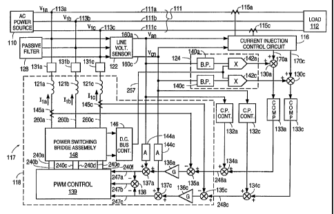
Fig. 3 is a three-phase circuit diagram depicting
active injection mode filter liZin accordance with one
embodiment of the present invention. Active injection
mode filter 117 is connected to a three-phase AC power
system. As illustrated in Fig. 3, three-phase AC power
source 110 is connected to three-phase, three-wire AC
load 112 by power line 111. Three-phase power line 111
includes conductors llla, 111b and lllc. AC power
source 110 provides line-to-ground voltages V1" V,b and
V1~ on conductors llla, lllb and lllc, respectively. In
a typical 480 volt line-to-line power distribution
system, the line-to-ground voltages V," V,b and Vt~ are
approximately 277 volts. Active current injection
device 117 is connected to conductors llla, 111b and
lllc of power line 111 at nodes 113a, 113b and 113c,
respectively.
Active current injection device 117 includes
impedances 131a, 131b and 131c, three-phase
transconductance power amplifier 118, line voltage
sensing circuit 122, power supply means 124, current
pump control circuits 132a and 132c, compensation
circuits 133a and 133c, passive filter 128, sensors
115a and 115-c, current injection signal generator 116,
and summing junctions 130a, 130c, 134a and 134c.
-12-
WO 95/34119 2 t 9 2 ~ 8 9 PCT/US95106875
Three-phase transconductance power amplifier 118
includes pulse width modulation control circuit 139,
three-phase power switching bridge assembly 148, DC bus
voltage control circuit 146, transducers 145a and 145c,
impedances 121a-121c, amplifiers 136a and 136c,
attenuator circuits 144a and 144c and summing nodes
135a, 135c, 137a, 137c and 138.
Transconductance amplifier 118 generates three
output injection currents, I," I,b and I,~, in response
to two input voltage signals received from summing
nodes 134a and 134c. The three output injection
currents, I," hb and Il~, are transmitted from
transconductance amplifier 118, through impedances
131a, 131b and 131c, respectively, to nodes 113a, 113b
and 113c, respectively. Output injection currents I1"
I,b and I,~ each include several current components,
including fundamental frequency components and non-
fundamental frequency components. These output
injection current components are discussed later in
more detail.
Transconductance amplifier 118 receives input
voltage signals from summing nodes 134a and 134c which
are representative of the desired output injection
currents I1" hb and h~ on output leads 260a, 260b and
260c, respectively. The input voltage signals are
described in more detail later in the specification.
The input voltage signal from summing node 134a,
which is representative of the desired output injection
current I," is transmitted through summing node 135a,
amplifier 136a and summing node 137a to input lead 247a
of. pulse width modulation control circuit 139.
Similarly, the input voltage signal from summing node
134c, which is representative of the desired output
injection current I,~, is transmitted through summing
node 135c, amplifier 136c and summing node 137c to
input lead 247c of pulse width modulation control
-13-
WO 95134119 ,, ,, , ~ ", 219 21 g 9 PCTIUS95106875
circuit 139.-_The outputs of summing nodes 137a and
137c are combined in summing node 138 to form a third
input voltage signal which is equal to the negative sum
of the outputs of summing nodes 137a and 137c. This
third input voltage signal is provided to pulse width
modulation control circuit 139 on input lead 247b.
The pulse width modulation control circuit 139
provides drive signals to power switching bridge
assembly 148 on leads 240a-240f. In response, power
switching bridge assembly 148generates output injection
currents I1" I,b and I,~ on leads 260a, 260b and 260c,
respectively.
The output injection currents from power switching
bridge assembly 148 are controlled by a current control
negative feedback loop formed by using transducers 145a
and 145c (which are coupled to output leads 260a and
260c, respectively) to provide signals representative
of output injection currents II, and II~ to the negative
inputs of summing nodes 135a and 135c, respectively.
Because the current control feedback loop has finite
gain, transconductance amplifier 118 performs like an
ideal transconductance amplifier with an effective
parallel impedance Z~.
The output injection currents I," I,b and I,~ on
leads 260a, 260b and 260c are filtered by output
inductors 121a, 121b and 121c and shunt passive filter
128 to remove switching frequency components generated
by power switching bridge circuit 148. Consequently,
the output injection currents I,, and I,~ are
proportional to the voltage signals received on input
leads 248a and 248c, respectively, and I,b = -(I1,+Ia)
Summing nodes 137a and 137c also receive input
signals from attenuating circuits 144a and 144c,
respectively. Attenuator circuits 144a and 144c
receive input signals from leads 160a and 160c of line
voltage sensor 122. As discussed later, the voltages
-14-
W0 95134119 PCTIUS95106875
.. ., ..2182189
Vm and V~~ on leads 160a and ibOc are representative of
the line-to-neutral voltages Vlm and V~~" at nodes 113a ,
and 113c, respectively. The output of attenuator
circuits 144a and 144c are line voltage feed forward
signals inside the current control feedback loop that
reduce the necessary loop gain of the current control
feedback loop, thereby improving control over the
output injection currents I1" IIy and Im and increasing
the stability of the feedback loop. In the prior art,
where the output of the transconductance amplifier was
connected directly to the AC power line, the required
effect of the voltage feed forward was significant. In
the present invention, however, the output of
transconductance amplifier 118 sees little or none of
the AC power line voltage as a result of the voltage
drops across impedances 131a-131c. Consequently, the
amount of voltage feed forward needed is substantially
reduced. In other embodiments, attenuator circuits
144a and 144c are eliminated, thereby eliminating the
voltage feed forward signals.
Fig. 4 is a circuit diagram of one embodiment of
pulse width modulation control circuit 139. Triangular
wave oscillator 248 generates a triangular wave voltage
VT at a frequency f~. The frequency f~ is typically 20
kHz, which is approximately 10 times the highest
frequency component to be generated by the
transconductance amplifier 118. Triangular wave VT is
applied to the inverting inputs of analog comparators
249a-249c. The outputs of summing nodes 137a, 138 and
137c are applied to the non-inverting inputs of analog
comparators 249a, 249b and 249c, respectively. The
two-state output signals of comparators 249a, 249b and
249c are routed through inverters 250a-25oc and drive
circuits 251a-251f, thereby producing drive signals on
leads 240a-240f. The drive signals on leads 240a-240f
are provided to power switching bridge circuit 148.
-15-
WO 95134119 PCTIUS95/06875
. .,: x.:2092189 .
Fig. 5 is a circuit diagram illustrating one
embodiment of power switching bridge circuit 148. The
signals on leads 240a-240f are provided to the bases of
power semiconductor switches 250a-250f, respectively.
Diodes 251a-251f are connected between the collectors
and emitters of switches 250a-250f, respectively. The
collectors of-switches 250a, 250c and 250e are
connected to the positive DC bus 246a. The emitters of
switches 250a; 250c and 25-Oe are connected to the
collectors of switches 250b, 250d and 250f,
respectively and to output leads 260a, 260b and 260c,
respectively. The emitters of switches 250b, 250d and
250f are connected to the negative DC bus 246b.
Capacitor 241...is connected between DC buses 246a and
246b. A DC voltage VDT, exists between DC buses 246a
and 246b.
The signals applied to leads 240a-240f open and
close switches 250a-250f to connect the output leads
260a-260c to either DC bus 246a or DC bus 246b, thereby
causing output injection currents I," Iib and I,~ to flow
on leads 260a-260c.
Line voltage sensing circuit 122 xeceives line-to-
ground voltages Vi,, V,b and V,~ from nodes 113a-113c,
respectively. In response, line voltage sensing
circuit 122 provides two output signals V,~ and V~ on
leads 160a and 160c, respectively. The output signals
V,~ and V~ are-used to control various circuits within
active current injection device 117. V,~ is
proportional to Vi,-Vo and V~ is proportional to Vl~ Vn,
where Vo is equal to (V,,+V~b+V,~) /3. Thus, Vo is
representative of a neutral-to-ground voltage for power
line 111 and V,~ and V~ are representative of line-to-
neutral voltages V,,~ and Vl~, of conductors 111a and
lllc, respectively. Line-to-neutral voltage V,ti~ is
equal to -(V,,~ + Vl~o)
Fig. 6 is a circuit diagram of one embodiment of
-16-
W095134119 ~ : PCTlUS95/06875
line voltage sensing circuit--122. Line-to-ground
voltage Via from node 113a is applied to the inverting
attenuator consisting of attenuation control resistors
R1a and R2a and operational amplifier 155a. Similarly,
line-to-ground voltage V,b from node 113b is applied to
the inverting attenuator consisting of resistors R1b
and R2b and operational amplifier 155b, and line-to-
ground voltage Vt~ from node 113c is applied to the
inverting attenuator consisting of resistors Rlc and
R2c and operational amplifier 155c. In one embodiment,
resistors Rla, Rlb and R1c all have the same resistance
and resistors R2a, R2b and R2c all have the same
resistance.
The outputs ofoperational amplifiers 155a, 155b
and 155c are transmitted through equal-value resistors
R3a, R3b and R3c, respectively, to node 157. The
voltage on node 157 is equal to the average of the
voltages on the outputs of operational amplifiers 155a,
155b and 155c. Node 157 and the output of operational
amplifier 155a are connected to the non-inverting and
inverting inputs, respectively, of unity-gain
differential amplifier 156a to produce output signal Vm
on lead 160a. Similarly, node 157 and the output of
operational amplifier 155c are connected to the non-
inverting and inverting inputs, respectively, of unity-
gain differential amplifier 156c to produce output
signal V~ on lead 160c. As previously discussed, V~,
and V~ are representative of the line-to-neutral
voltages V~,~ and V~~ on nodes 113a and 113c,
respectively.
Fig. 7 is a circuit diagram illustrating circuitry
within DC bus control circuit 146 in accordance with
one embodiment of the present invention. DC bus
control circuit 146 cooperates with power supply means
124 to control the voltage Vp~ across storage capacitor
241 in the power switching bridge assembly (i.e. the
-17-
W 0 95/34119 PCTIUS95l06875
~.~.19,2189
voltage between the positive DC bus 246a and the
negative DC bus 246b in that assembly), thereby
providing the power necessary to operate power
switching bridge assembly 148.
DC bus control circuit 146 uses operational
amplifier 164 in conjunction with resistors R12-R15 and
capacitors C6 and C7, to form a high-rejection common-
mode amplifier to produce an output signal proportional
to Vp~. This output signal is provided to the inverting
input of operational amplifier l65 through resistor ~
R16. Voltage reference source 166 provides to the
inverting input of operational amplifier 165 through
resistor R17 a signal representative of the desired
value of VD~.Resistor R18 and capacitors C8 and C9 are
connected across the inverting input and the output of
operational amplifier 165, thereby creating an
amplifier having an output proportional to the
difference between the voltage from operational
amplifier 164, which is representative of VDT and the
voltage from voltage reference source 166, which is
representative of the desired value of Vp~. Thus, if
the voltage VDT is equal to the desired value, the
output on lead 257 is zero. If VDT is less than the
desired value, the output signal on lead 257 is less
than zero. Conversely, if VDT is greater than the
desired value, the output signal on lead 257 is greater
than zero. Lead 257 is connected to multipliers 142a
and 142c of power supply means 124.
In response to the output signal on lead 257 and
the voltages V~ and V~ from line voltage sensing
circuit 122, power supply means 124 causes
transconductance amplifier 118 to generate a current
component at the fundamental frequency to maintain the
desired voltage VDT between DC buses 246a and 246b.
This current component is normally opposite in phase to
the power line voltage at nodes 113a-113c, thereby
-18-
WO 95134119 ~ i ~ ~ ~ ~ ~ PCTIUS95/06875
,e
causing power to flow from nodes 113a-113c to the DC
buses 246a and 246b through impedances 131a-131c,
inductors 121a-121c and semiconductor power switches
250a-250f to maintain the desired DC bus voltage across
DC buses 246a and 246b.
Power supply means 124 includes band-pass filters
140a and 140c and multipliers 142a and 142c (Fig. 3).
Leads 160a and l6oc of line voltage sensing circuit 122
are connected to the inputs of band-pass filters 140a
and 140b, respectively. Band-pass filters 140a and
140c pass the fundamental frequency components of
voltages V,~ and VW, respectively, to multipliers 142a
and 142c, respectively. Band-pass filters 140a and
140c are conventional filters. Fig. 8 is a circuit
diagram of one embodiment of band-pass filter l4oa. In
this embodiment, band-pass filter 140a is identical to
band-pass filter 140c. The values of resistors R9a and
RlOa and capacitors C3a and C4a are selected to produce
zero phase shift at the fundamental frequency and
attenuation at non-fundamental frequencies.
Multipliers 142a and 142c also receive the output
of DC bus voltage controller 146 on lead 257. As
previously discussed, the output of DC bus voltage
controller 146 is a voltage representative of the
difference between the desired voltage across DC buses
246a and 246b and the actual voltage VDT between DC
buses 246a and 246b (i.e. across storage capacitor
C241). If this difference is zero, the outputs of
multipliers 142a and 142c are also zero, and power
supply means 124 does not cause any power to flow from
nodes 113a-113c to the DC buses 246a and 246b.
However, if the output of DC bus control circuit 146
indicates that the voltage VDT is less than the desired
value, multipliers 142a and 142c generate voltage
signals at the fundamental frequency which are opposite
in phase to the fundamental frequency components of
-19-
W~ 95134119 PCT/U595/06875
'2y..92189
power line voltages V,~ and VI". The outputs of
multipliers 142a and 142c are provided to
transconductance amplifier 118 through summing nodes
130a and 130c, respectively, and compensation blocks
133a and 133c, respectively. In response,
transconductance amplifier 118 generates current
components of currents I,o, I,b and I,~ at the fundamental
frequency which results in a flow of power from power
line 111 to capacitor 241 which increases the voltage
to vD~.
Conversely, if the output of DC bus control
circuit 146 indicates that the voltage VDT is greater
than the desired value, multipliers 142a and 142c
generate voltage signalsat the fundamental frequency
which are in phase with the fundamental frequency
components of power line voltages V1" and V,~a. Under
these circumstances, the outputs of multipliers 142a
and 142c cause transconductance amplifier 118 to
generate current components of currents I," I,b and Il
at the fundamental frequency resulting in a flow of
power from capacitor 241 to power line 111, thereby
discharging capacitor 241 and decreasing VDC~
The output signals V" and V~ on leads 160a and
l6oc of line voltage sensing circuit 122 are also
provided to current pump control circuits 132a and
132c. Current pump control circuits 132a and 132c
generate voltage signals proportional to the
fundamental frequency components of voltages V1~ and
V1~, respectively, but lagging in phase by 90 degrees.
These lagging voltage signals are provided to
transconductance amplifier 118, resulting in the
generation of components of currents I," I,b and I,
which lag the line voltages V,,~, V,~ and Vl~ by 90
degrees. These lagging currents result in
corresponding voltage drops across impedances 131a-131c
which are approximately equal to the fundamental
-20-
WO 95/34119 PCTIUS95106875
rv ~ ''~ 192189
frequency voltage components of the line voltage. As
previously discussed, these voltage drops reduce the
required DC operating voltage VDT of the power switching -
bridge assembly 148 and supply leading current to power
line 111. It is preferred that VDT be less than 600
Volts, thereby allowing the use of less inexpensive
switching transistors and reducing switching losses.
The output voltages of current pump controls 132a
and 132c are selected so that
IIaCP*ZPa '~' VlaW
IIbCP*fPb ~ Ulbni and
IlccP* 'LPc ~ Ulrn
In the above listed equations, I,,~, IlbcP and II~cP are the
components of output injection currents I," I~b and II~,
respectively, which are generated by transconductance
amplifier 118 in response to the output voltage signals
of current pump controls 132a and 132c. ZPa, Z~ and Z~
are the respective impedances of impedances 131a, 131b
and 131c at the fundamental frequency, and V,,~, Vlbo and
Vl~n are the line-to-neutral voltages of power line 111
at respective nodes 113a, 113b and 113c.
In one embodiment impedances 131a, 131b and 131c
are matched impedance capacitors. In other
embodiments, impedances 131a-131c are capacitors and
inductors connected in parallel.
Fig. 9 is a circuit diagram of one embodiment of
current pump control circuit 132a. In this embodiment,
current pump control circuit 132c is identical to
current pump control circuit 132a. Lead 160a couples
the V,~ output of line voltage sensing circuit 122 to
the input of a two-pole analog active filter circuit
consisting of operational amplifier 162a, resistors
R4a-R6a, and capacitors Cla and C2a. The values of
resistors R4a-R6a and capacitors C1a and C2a are chosen
such that the output of operational amplifier 162a has
a phase shift of positive 90 degrees with respect to
-21-
W 0 95134119 PCT1US95l06875
the V,~ signal. The two-pole analog filter circuit also
provides substantial attenuation for non-fundamental
frequencies, such that the output of the filter circuit
is proportional to the fundamental frequency component
of V". Operational amplifier 161a in conjunction with
resistors R7a and R8a inverts the output of operational
amplifier 162a to produce an output voltage which,
because of the inversion, has a 90 degree phase lag
with respect-to the V" signal. The values of resistors
R4a-R8a and capacitors C1a-C2a are selected such that
the above-listed requirements are satisfied.
Current injection signal generator 116 has two
functions in the embodiment illustrated in Fig. 3. The
first function is to generate voltage signals which are
ultimately provided to transconductance amplifier ll8
to create non-fundamental frequency current components
of output currents I1" I,b and I~~. The generated non-
fundamental frequency current components are equal to
the non-fundamental frequency components drawn by load
112. Consequently, the non-fundamental frequency
current components of load 112 are not drawn from AC
power source 110.
However, when the non-fundamental frequency
current components flowing to load 112 exist because of
non-fundamental frequency voltages on AC power line
111, and not because of non-linearity of load 112, the
first function by itself unloads the non-fundamental
frequency voltages from AC power line 111, resulting in
an increase in the amplitude of non-fundamental
frequency voltages in other equipment (not shown)
connected to the power system. When load 112 contains
capacitive elements, the first function can cause
system instability.
Hence, the second function of current injection
signal generator 116 is to counteract the unloading of
non-fundamental frequency voltages and resulting
-22-
W0 95/34119 PCT/US95f06875
''°~~921~9
instability. This second function is performed by
using-damping control circuits within current injection
signal generator 116 to generate voltage signals which
are ultimately provided to transconductance amplifier
118 to create non-fundamental frequency current
components of output injection currents I," I16 and I,
These non-fundamental frequency current components are
approximately opposite in phase to the power line
voltages V,,~, V,eo and V,~a and thereby load the non-
fundamental frequency voltage components of these
voltages.
Fig. 10 is a block diagram of one embodiment of
current injection control circuit 116. Current
transducers 115a and 115c sense the currents on
conductors 111a and lllc, respectively, and provide
signals representative of these currents to positive
inputs of summing nodes 177a and 177c, respectively.
Damping control circuits 176a and 176c receive input
signals V" and V~o from leads 160a and 160c of line
voltage sensor 122. The outputs of damping control
circuits 176a and 176c are representative of electronic
loadings which are created for the non-fundamental
frequency voltage components of voltages V,o and V,o.
The outputs of damping circuits 176a and 176c are
provided to negative inputs of summing nodes 177a and
177c, respectively.
The outputs of summing nodes 177a and 177c are
provided to inputs of notch filters 178a and 178c,
respectively. Notch filters 178a and 178c filter the
signals from summing nodes 177a and 177c, respectively,
to remove the fundamental frequency component. Fig. 11
is a circuit diagram illustrating one embodiment of
notch filter 178a. In this embodiment, notch filter
178c is identical to notch filter 178a. Notch filter
178a is a conventional circuit which uses operational
amplifiers 185a and 186a and resistors R43a and R44a to
-23-
WO 95134119 ~ 19 218 9 PCTIUS95106875
provide positive feedback to the "T" element of the
notch filter formed by capacitors C25a-C27a and
resistors R40a-R42a. The outputs of notch filters 178a
and 178c are provided to summing nodes 130a and 130c,
respectively on leads 170a and 170c, respectively.
The signals from sensors 115a and 115c perform the
first function of current injection signal generator
116 described above. The signals from damping control
circuits 176a and 176c perform the second function of
the current injection signal generator 116.
Fig. 12 is a circuit diagram illustrating one
embodiment of damping control circuit 176a. In this
embodiment, damping control circuit 176c is identical
to damping circuit 176a. The input voltage signal V,
on lead 160a is inverted by the inverter formed by
operational amplifier 180a and resistors R30a and R3la.
The output of operational amplifier 180a is provided to
the inverting input of operational amplifier 182a
through a high pass filter formed by capacitor C22a and
resistor R33a. Resistor R33a and capacitor C22a are
selected so that at the frequencies of interest (i.e.,
100 to 2000 Hz), the impedance of resistor R33a is much
larger than the impedance of capacitor C22a, such that
the effects of resistor R33a dominate. In one
embodiment, the time constant of the high pass filter
formed by capacitor C22a and resistor R33a is
approximately 1 msec.
The output of operational amplifier 180a is also
provided to the inverting input of operational
amplifier 182a through variable resistor R32a,
operational amplifier 181a, and a high pass filter
formed by capacitor C23a and resistor R34a. Resistor
R34a and capacitor C23a are selected so that at the
frequencies of interest, the impedance of capacitor
C23a is much larger than the impedance of resistor
R34a, such that the effects of capacitor C23a dominate.
-24-
WO 95134119 ~' ~ ~ y' g 2 j 8 9 PCT/US95106875
In one embodiment, the time constant of the high pass
filter formed by capacitor C23a and resistor R34a is
approximately 0.1 msec.
Resistor R35a is connected to the inverting input
and the output of operational amplifier 182a. The
output of operational amplifier 182a is a voltage
signal with two components. The first component, which
is proportional to line voltage V~,~, results from
applying a voltage across resistor R33a. The second
component, which is proportional to the rate of change
of line voltage V1,~, results from applying a voltage
across capacitor C23a.
The fundamental frequency components of the
outputs of damping control circuits 176a and 176c are
removed by notch filters 178a and 178c, thereby
transmitting the non-fundamental frequency components
of these outputs through compensation blocks 133a and
133c to transconductance amplifier 118. In response,
transconductance amplifier 118 generates non-
fundamental frequency current components of I,a, I16 and
I1~ which are a function of, and approximately opposite
in phase with respect to, the non-fundamental frequency
voltage components of the line voltages V,,~, V,b" and V,~.
Thus, for each volt of non-fundamental frequency
voltage present on power line 111, damping control
circuits 176a and 176c cause active current injection
device 117 to draw a frequency-dependent non-
fundamental frequency current. In this manner, damping
control circuits 176a and 176c create an electronic
load, ZE, for non-fundamental frequency voltages.
Electronic load ZE has two components, ZR and Z~, where
ZR is a resistive component determined by the resistor
R35a and Z~ is a capacitive component determined by
capacitor C23a.
Because active current injection device 117 also
generates the non-fundamental frequency currents
-25-
WO 95/34119 PCT/U595106875
:2.192189
required by load 112, the equivalent impedance of
active current injection device 117 and load 112 at
non-fundamental frequency voltages is equal to ZE.
Thus, unlike prior art AIM filters, active current
injection device 117 does not unload the non-
fundamental frequency voltages. Consequently, the
increased non-fundamental and frequency voltages and
instability experienced by prior art AIM filters is
eliminated.
In one embodiment of the present invention, the
electronic load ZE is selected to approximate the
impedance ZL of the linear elements of load 112 at non-
fundamental frequencies. To set ZE equal to ZL, the
value of resistor R33a of damping control circuit 176a
is selected to correspond to the resistive component of
Zy and the value of capacitor C23a of damping control
circuit 176a is set to correspond to the capacitive
component of ZL. If ZL has no capacitive component,
variable resistor R32a of damping control circuit 176a
is set to ground the input to capacitor C23a and avoid
instabilities.
The outputs of current injection control circuit
116 (i.e. the outputs of notch filters 178a and 178c)
are added to the outputs of power supply means 124
(i.e. the outputs of multipliers 142a and 142c,
respectively) at summing nodes 130a and 130c,
respectively. The outputs of summing nodes 130a and
130c are provided to inputs of compensation circuits
133a and 133c, respectively.
Compensation circuits 133a and 133c provide
amplitude and phase correction to the outputs of nodes
130a and 130c to compensate for amplitude and/or phase
shift in the output injection currents I1" I,b and I,
caused by impedances 131a, 131b and 131c.
The desired transfer function for compensation
circuit 133a (or 133c) is given by
-26-
W 0 95/34119 ~ PCTIUS95106875
'~ 192189
vout/vin =- (ZP + ZA)/ZA
where ZP is the impedance of impedance 131a (or 131c)
and ZA is the equivalent output shunt impedance of
transconductance amplifier 118. Impedance 131a (or
131c) is typically a capacitor having a capacitance of
CP. As previously discussed, impedance ZA results from
the finite gain of the current feedback loop of
transconductance amplifier 118. At the frequencies at
which compensation is required, Z,, is principally
resistive with a resistance of RA. The impedances of
inductors 121a-121c are small enough at the frequencies
of interest to be ignored in determining the equivalent
output shunt impedance Z" of transconductance amplifier
118.
Fig.-13 is a circuit diagram of one embodiment of
compensation circuit 133a which provides the desired
transfer function. In this embodiment, compensation
circuit 133c is identical to compensation circuit 133a.
In compensation circuit 133a, the signal from
summing node 130a is provided to an amplifying inverter
formed by operational amplifier 173a, resistors R20a-
R22a and capacitor C20a.
To provide the desired transfer function, the
resistance of resistor R2la and the capacitance of
capacitor C20a are chosen such that the time constant
R2la * C20a is equal to the time constant RA * CP. The
resistance of resistor R20a is selected to correspond
to the resistance of R2la. The value of resistor R22a
is chosen to be large with respect to resistor R2la,
and acts to limit the compensation at frequencies below
the fundamental frequency.
The output of operational amplifier 173a is
inverted by the inverter formed by operational
amplifier 174a and resistors R23a and R24, thereby
providing an output signal having the proper lagging
phase. Given these circuit parameters, compensation
-27-
WO 95/34119 PC'fIUS95106875
,~ , _,~ 192189
circuit 133a provides the desired transfer function at
the frequencies of interest (i.e., 100 to 2000 Hz)
without providing excessive gain at frequencies less
than the fundamental frequency of the AC power line.
The outputs of compensation circuits 133a and 133c
are provided to positive inputs of summing nodes 134a
and 134c, respectively, where they are added to the
outputs of current pump controls 132a and 132c,
respectively, and transmitted to transconductance
amplifier 118.
Fig. 14 is a block diagram illustrating non-
fundamental frequency currents existing in the three-
wire, three-phase power system previously described in
connection with active current injection device 117.
The currents i~" iSb and is, represent the non-
fundamental-frequency components of the currents
flowing from source 110 to nodes 113a, 113b and 113c,
respectively. Currents i," ilb and i1~ represent the
non-fundamental-frequency components of the currents
flowing from active current injection device 117 to
nodes 113a, 113b and 113c, respectively. Currents i4,
iu, and iu represent the non-fundamental-frequency
components of the currents flowing to load 112 from
nodes 113a, 113b and 113c, respectively. In such a
power system, the following equations apply.
i~, + i~ + i~ = 0
i,a + i,6 + i,~ = 0
iya + 1iy + 1u = 0
18t = iLa -= ila
ice, = iu, - i~b and
i~ = i,~ - in.
Using the inputs from transducers 115a and 115c, active
current injection device 117 produces ila and il~ such
that, in the absence of non-fundamental frequency
voltage components of line voltages V,~" V~b" and Vt~",
i1a i~ and ilk iu, in which case, by the equations above,
-28-
W0 95134119 PCTIUS95106875
,;
hti lLbi and isa ise ls~ 0.
However, if the active current injection device
117 is coupled to a four-wire, three-phase system (with
a neutral wire being the fourth wire) without
modification, problems may arise. In a four-wire,
three-phase system, the following equations apply:
isa + isb + isc = in.
iL + i~ + iu = i~, and
lia + lay + 1~~
where io represents the non-fundamental-frequency
components of the current flowing in the neutral wire.
In this system, if the active current injection device
117 makes i~a i,., and ilk iu, then is, and is~ equal 0 and
isb equals ia, i.e., the total non-fundamental-frequency
component of the neutral wire current flows through
conductor 111b, thereby causing potential overheating
in that conductor and in upstream power distribution
transformers. Thus, in an alternate embodiment of the
present invention, the active current injection device
117 as previously described is modified for use in a
four-wire, three-phase power system.
Fig. 15 is a block diagram showing the connection
of a four-wire adapter circuit 200 for active current
injection device 117. In the four-wire, three-phase
embodiment, power line 111 includes neutral conductor
111n in addition to conductors 111a-111c. Neutral
conductor 111n provides a return path for the non-
fundamental frequency current component in from load
112 to power source 110. An additional transducer 115b
is coupled to conductor 111b. Transducers 115a, 115b
and 115c create signals whose non-fundamental frequency
components are proportional to currents iL, iv, and ice.
Four-wire adapter circuit 200 receives these signals
from transducers 115a, 115b and 115c.
Fig. 16 is a schematic diagram of four-wire
adapter circuit 200. The output of transducer 115a is
-29-
W0 95/34119 PCTIUS95106875
v ~~, ~ ~ 't
2192189
provided to a positive input of summing node 205a and
to a positiveinput of summing node 203. The output of
transducer 115b is provided to a positive input of
summing node 203. The output of transducer 115c is
provided to a positive input of summing node 205c and a
positive input of summing node 203. The output of
summing node 203 is divided by three by attenuator
circuit 204. The output of attenuator circuit 204 is
provided to negative inputs of summing nodes 2D5a and
205c. Thus, the output of summing node 205a is
proportional to i~, - (1/3 * i") and the output of
summing node 205c is proportional to i,~ - (1/3 * io).
The outputs of summing nodes 205a and 205c are
provided to summing nodes 177a and 177c, respectively,
of current injection control circuit 116 of active
current injection device 117 (Fig. 10). These outputs
are transmitted to transconductance amplifier 118
through notch filters 178a, 178c, compensation circuits
133a, 133c and summing nodes 130a, 130c, 134a and 134c
(Fig. 3). In response, transconductance amplifier 118
generates non-fundamental frequency current component
i,, which is equal to ii, - (1/3 * io) and non-fundamental
frequency current component i,~ which is equal to iu -
(1/3 * io). Based on the above-listed equations, non-
fundamental frequency current component i,b is generated
that is equal to iiy - (1/3 * ia) .
As a result, the non-fundamental frequency current
components i", i,b and i,~ on lines 111a-lllc are equal in
phase and amplitude to one another and equal to one
third of the non-fundamental frequency component in
neutral line llin. This is true even if the non-
fundamental current components of load 112 are
unbalanced (e. g., all of the non-fundamental current
components are drawn by one of the three phases). By
balancing the non-fundamental frequency current
components as previously described, the potential for
-30-
WO 95134119
PCT1US95106875
overheating upstream devices as a result of these
current components is reduced.
Although the present invention has been described
in accordance with certain embodiments, alternate
embodiments are contemplated. For example, although
the present invention has been described in accordance
with a three-phase embodiment, modifications could
easily be made to provide for a single phase
embodiment.
Additionally, although the present invention has
been described in an active injection mode embodiment,
the present invention can be easily modified to operate
in response to an independent signal generator. In
such an embodiment, transducers 115a and 115c are
disconnected from summing nodes 177a and 177c of
current injection control circuit 116 (Fig.lO) and the
independent signal generator is used to supply the
desired signals to summing nodes 177a and 177c. As
previously described, such an embodiment can be used to
test the tolerance of the power system to non-
fundamental frequency signals. Accordingly, the
present invention is only limited by the following
claims.
-31-
"', . , ~. , .::i~y;~~,~".