Note: Descriptions are shown in the official language in which they were submitted.
WO 9S13408~ 2 1 9 2 3 6 9 PC~U595/07420
RT,RCTTITC}~T, DRVICR~
This invention relates to devices comprising conductive polymer
elements, in particular electrical devices such as circuit protection
S devices in w~ic~ current flowL between two electrodes through a conductive
polymer element.
It i~ well known to make compositions which comprise a polymeric
component and, diLpersed therein, electrically conductive particIes. The
type and r~n~ntrAt;~n of the particles may be such that the composition is
conductive under normal conditions, e.g. has a resistivity of less than 106
ohm-cm at 23~C, or is ~ nt;Ally ;n~lllAt;ng under normal conditions, e.g.
has a resistivity of at least lO9 ohm-cm at 23~C, but has a non linear,
voltage-dependent resistivity such that the composition becomes conductive
if subjected to a sufficiently high voltage stress. The term ~conductive
polymer~ is used herein to describe all such compositions. When the
polymeric component comprises a crystalline polymer, the composition will
usually exhibit a sharp increase in resistivity over a relatively narrow
t~ _ ~ range just below the crystalline melting point of the polymer,
and such compositions are described aL PTC compositions, the abbreviation
~PTC" meaning positive t~ tl~re coefficient. The size of the increase
in resistivity is important in many uses of PTC compositions, and iA often
referred to as the ~autotherm height~ of the composition PTC conductive
polymers are particularly useful in circuit protection devices and self-
regulating heaters. Conductive polymers can contain one or more polymers,one or more conductive fillers, and optionally one or more other
ingredients such as inert fillers, stAhi~ rA~ and anti-tracking agents.
Particularly useful results have been obtained tbrough the use of carbon
black as a conductive filler.
For details of known or proposed conductive polymers and devioes
rnntA;n;ng them, reference may be made, for example, to the documents
incorporated herein by reference in the Detailed D~A~r;pt;~n of the
Invention below.
~5
When a melt-processed, sintered, or otherwise shaped conductive
polymer element is to be divided into smaller pieces, this has in the past
been achieved by shearing ~also referred to as:"dicing") the conductive
polymer element. For example, many circuit protection devices are made by
WO 95/3~08~ 2 1 9 2 3 6 9 PCrNS9~107420
.
-2- ~ .
Hhearlng a laminate compri6ing two metal foils and a laminar PTC conductive
polymer element sandwiched between the foil6. ~ ~
We have discovered, in accordance with the present invention, that in
S many cases, important advantages can be obtained by dividing a conductive
polymer mass into a plurality of parts by a proceas in which at least part
of the division is effected by causing the conductive polymer element to
break, along a desired path, without the introduction of any solid body
into the conductive polymer element along that path. The resulting
cohesive failure of the conductive polymer produces a surface (referred to
herein as a ~fractured~ surface) which is distinctly different from that
produced by a shearing process, which necessarily results in deformation of
the conductive polymer by the cutting body. In order to~contrQl the path
along which the conductive polymer element breaks, we prefer to provide one
or more fl;crnnt;nl-;ties which are present in one or more members 6ecured to
the conductive polymer, and/or in the conductive polymer it6elf, and who6e
presence causes the conductive polymer to fracture along desired paths
which are related to the fl;~cnnt;nll;ties.
The invention preferably makes use of assemblie6 in which a conductive
polymer element i6 sandwiched between metal members having physical
fl~crnnt;nll;tie5 in the form of channels. When such an assembly is bent in
the regions of the channels, the conductive polymer element will fracture
along patha which run between the ~u~ iing channels in the metal
members. ~owever, the invention includes the use of other types of
physical fl;Rrnnt;n~;ty and other kinds of fl;cnnnt;ml;ty which will interact
with a physical or other force to cause fracture of the conductive polymer
along a desired path.
We have found the present invention to be particularly u6eful for the
production of devices from a laminar as6embly comprising a laminar PTC
conductive polymer element c~nflw; rhrfl between metal foil6. we have found
that such devices, especially when they are small ~e.g. have an area of
less than 0.05 inch~ (32 mml)), generally have a slightly higher resi6tance
3s and a substantially higher autotherm height than similar devices produced
by the conventional shearing procesL. The invention i6 particularly useful
W O 95/34084 2 1 9 2 3 6 q PC~rrUS95/07420
.
--3--
for the production of devices of the kind degcribed in Tnt~rn~tl nnAl
Application No. PC~/Us34/lol37 (p.lhl;rAt;nn No. wo gs/00176).
In one preferred aspect, the present invention provides a device
s comprising an element which
(a) is composed of a composition which comprise~ (i) a polymeric
component and (ii), dispersed in the polymer, electrically
conductive particles, and
(b) has at least one fractured surface.
A preferred ~ of this aspect of this invention is a device which
comprises
(1) a laminar conductive polymer element which
(a) i8 composed of a composition which comprises (i) the
polymeric component and (ii) the ~l~ctr~rAlly conductive
particles in an amount such that the composition has a
resistivity at 23~C of less than lo6 ohm-cm, and
(b) has a first principal face, a second principal face parallel
to the first face, and at least one ~L~ eL~ face which
runs between the first and second faces and at least a part
of which has a fractured surface;
(2) a first laminar electrode which has (i) an inner face which
contacts the first principal face of the conductive polymer
element, and (ii) an outer face; and
~3) a second laminar electrode which has (i) an inner face which
contacts the second principal face of the conductive polymer
element, and (ii) an outer face.
~ :
In another preferred aspect, the present invention provides a method
of making a deYice, which method comprises
W O95/3408~ 21 92~6 9 r~"~,r. ,420
.
_q_
~1~ making an assembly which (a) comprise3 an element composed of a
composition comprising ~i) a polymeric component, and (ii),
dispersed in the polymeric component, ~lrctr;rAlly conductive
S particles, and (b) has one or more ~ rnnt;ml;ties in or adiacent
to the conductive polymer element; and
(2) separating the assembly into two or more parts by a treatment
which causes cohesive failure of the conductive polymer element
along a path which is related to the ~;Arrnt;nl-;ty.
A preferred ~ ' ~ m nt of this aspect of the invention is a method wherein
the assem.~bly comprises
(A) a laminar conductive polymer element which
(a) is composed of a _ ~ t; ~n which comprises a polymeric
component and, dispersed in the polymeric component,
electrically conductive particles in an amount such that the
composition has a resistivity at 23~C of less than 1o6 ohm-cm,
and
(b) has a first principal face and a second principal face
parallel to the first face,
~ ~ :
(B) a plurality of upper laminar conductive members, each of which has
(a) an inner face which contacts the first principal face of the
conductive polymer element and (b) an outer face, the upper
conductive members defining, with ;"r~rm~;At~ portions of the
conductive polymer element, a plurality of upper fracture
channels, and
(C) a plurality of lower laminar conductive members, each of which has
(a) an inner face which contacts the second principal face of the
conductive polymer element, and (b) an outer face, the lower
conductive members defining, with ;ntl ';At~ portions of the
WO 95/34084 2 ~ 12 ~ 6 9 PCT~US95~07420
conductive polymer element, a plurality oi lower fracture
channels; and
wherein step (2) of the process compri~es applylng physical forces to the
assembly which cause the conductive polymer eLement to fracture along a
plurality of paths each of which runs between one of the upper fracture
channels and one of the lower fracture channels.
In another preferred aspect, this invention provides an assembly which
can be divided into a plurality of deviceg by method of the invention, and
which comprises
(A) a laminar conductive polymer element which
(a) is composed of a composition which comprises a polymeric
component and, dispersed in the polymeric component,
PlP~tr;~11y conductive particles, and
(b) has a first principal face and a second principal face
parallel to the first face,
(}3) a plurality of upper laminar conductive members, each of which has
(a) an inner face which contacts the first principal face of the
conductive polymer element and (b) an outer face, the upper
conductive members defining, with ;ntPrnP~;~t~ portions of the
conductive polymer element, a plurality of upper fracture
channels, and
(C) a plurality of lower laminar conductive members, each of which has
(a) an Inner iace which contacts the second principal face of the
conductive polymer element, and (b) an outer face, the lower
conductive members defining, with ;ntl ''~tP portions of the
,~ conductive polymer element, a plurality of lower fracture
channels.
The invention is described below chiefly by reference to PTC circuit
prnte~t; nn devices which comprise a laminar PTC element composed of a PTC
W 0 95/34084 1 9 2 3 6 9 PCTrU595/07420
conductive polymer and two laminar electrodes secured directly to the PTC
element, and to methods for producing such devices in which a laminar
element having surface ~;urnnt;nn;ties is subjected to physical forces
which bend the element 50 as to cause cohesive iailure of the conductive
polymer. It is to be nn~rrrtnn~, however, that the description is also
Aprl;rAhle, insofar as the context permits, to other electrical devices
rnntA;n;ng conductive polymer elements and to other methods.
As described and claimed below, and as illustrated in the
IO Al ying drawings, and as further described and illustrated in the
documents incorporated herein by reference, the present invention can make
use of a number of particular features. Where such a feature is disclosed
in a particular context or as part of a particular ~ ~;nAt;nn, it can also
be used in other contexts and in other ,1nAt;nn~, including for example
other ~ ' nAt;nnq of two or more such features.
Any conductive polymer can be used in this invention, providing it is
present in the form of an clement which can be subjected to physical and/or
other forces which will cause the element to undergo the cohesive failure
which results in a fractured surface. The more brittle the conductive
polymer, the easier it is to obtain this result. We have obtained
excellent results using conductive poIymers rnntAln;ng high proportions of
c~rbon black, e.g. at least 40~ by weight of the composition. When the
conductive polymer will not snap easily, a variety of ~rrP~;rntc can be
used to assist in achieving the desired result. For example, the
composition can be rrf~ 1 At~ to include ingredients which render it more
brittle, or it can be shaped into the element in a different way. The
lower the t~ ,/eL~LULe, the more brittle the conductive polymer, and in some
cases it may be desirable to chill the conductive polymer element to a
30 t~ _ ~LUL~ below ambient temperature before breaking it, e.g. by passing
it through li~uid nitrogen. Compositions in which the polymeric component
consists P~nt;Ally of one or more crystalline polymers can usually be
fractured without difficulty at t- - - LUL~ substantially below the
crystalline melting point. If the polymeric component consists of, or~
3S contains s.-h~tAnt;Al amounts of, an amorphgus polymer, the element is
preferably snapped at a t~ - ~ below the glass transition point of the
amorphous polymer. crnQAl ;nk;ng of the conductive polymer can make it more
W O 95/34084 2 1 9 2 3 6 9 PCTrUS95/07420
.
_7_
or less brittle, depending upon the nature of the polymeric component, the
type of crnqql;nk;ng process, and the extent of the crnqcl;nk;ng. The
quantity of carbon black, or other conductive filler, in the conductive
polymer must be such that the composition has the required resictivity for
the particular device. The resistivity iG, in general, as low as possible
for circuit protection devices, e.y. below 10 ohm-cm, preferably below 5
ohm-cm, particularly below 2 ohm-cm, and Dubstantially higher for heaters,
e.g. 102-lOh, preferably 103-106~ ohm-cm.
Suitable conductive polymer compositions are disclosed for example in
U.s. Patent Nos. 4,237,441 (van Konynenburg et al), 4,38B,607 ~Toy et al~,
4,470,898 ~Penneck et al), 4,534,8B9 ~van KV.IYII~bULY et al), 4,s4s,926
(Fout6 et al), 4,s60,49B ~orsma et al), 4,591,700 (Sopory), 4,724,417 (Au
et al), 4,774,024 (Deep et al), 4,77s,77B (van Konynenburg et al),
15 4,B59,B36 (Lunk et al), 4,534,156 (van Kv~yllel~uLy et al), 5,049,B50 (Evans
et al), 5,17B,797 (Evans et al), 5,250,226 (oswal et al), 5,250,22B
~3aigrie et al), and 5,37B,407 ~Chandler et al).
The conductive polymer i9 preferably present in the form of a laminar
element haviny two principal faces which are parallel to each other and to
which metal members are preferably attached. In many cases, the metal
member6 are metal foils. Particularly suitable metal foils are diqclosed
in U.S. Patents Nos. 4,6B9,475 ~Matthiesen) and 4,B00,253 ~Kleiner et al).
The laminar conductxve polymer element can be of any thickness which can be
25 snapped, but is preferably les6 than 0.25 inch (6.35 mm), particularly less
than 0.1 inch ~2.5 mm), eepecially less than 0.05 inch ~1.25 mm), thick.
The ~;q~nnt;nn;tie3 which are present in the ~ q of the
invention are preferably present in memberG which are secured to the
principal facee of the conductive polymer element, so that, in the devices
prepared from the assembly, the tlCUI~ n faces of the conductive polymer
element consist ~qq~nt;~lly of fractured eurfacec. Preferably the
~;q~nnt;nn;tieS are nnnt;nnn~1q channels produced by etching a metal member
so that it is separated into distinct _egments, with the conductive polymer
exposed at the bottom of the channel. ~owever, the invention includes the
use of ~;qnnnt;nn;t;~q which are entirely within or formed in a surface of
the conductive polymer, or which extend from members secured to the
_ _ . . , ...... . .. ~ _ _ _ _ _ _ _ . . .
W O 95/34084 PCT~US95107420
21 92369
--8--
conductive polymer element into the conductive polymer eLement, for example
channels routed through a metal member and partially into a conductive
polymer element to which it i6 attached. In such cases, the LL~I~.vel~e
face will be partially sheared and partially fractured.
When there is a metal member secured to only one of the principal
faces of the conductive polymer element, there need be ~;rrnrtinll;ties on
one 6ide only of the assembly. When there are metal members secured to
both principal faces, ~;~cnnt;m~;ties are needed in each metal member,
positioned so that the conductive polymer will fracture along a path
between the ~;qrnnt;nn;ties. The ~;rrnnt;n~;ties can be directly opposite
to each other, so that the transverse fractured face meets the principal
faces at a right angle, or offset from each other 8C that the LL~I.~v~L~e
fractured face meets one of the principal faces at an angle le6s than go ,
15 e.g. 30~ to 90~, preferably 45~ to 90~, particularly 60C to 90~, and the
other principal face at the complementary angle which is greater than 9o~,
e.g. 90~ to 150~. The increased path length will influence the rlrrtr;r~l
properties of the device.
The invention can be used to make a wide variety of devices, but is
particularly useful for making small devices, in which the edge properties
of the conductive polymer element play a more important part than in large
devices. The invention is especially useful for making circuit protection
devices, e.g. those disclosed in U.S. Patent Nos. 4,238,812 (Middleman et
25 al), 4,255,798 (Simon), 4,272,471 (Walker), 4,315,237 (Middleman et al),
4,317,027 (Middleman et al~, 4,329,726 (Miadleman et al), 4,330,703 (Horsma
et al), 4,426,633 (Taylor), 4,475,138 (Middleman et al), 4,472,417 ~Au et
~1), 4,689,475 (~tt~;r~Pn), 4,780,598 (Fahey et al), 4,800,253 (~leiner
et al), 4,845,838 (~acobs et al), 4,857,880 (Au et al), 4,907,340 (Fang et
30 al), 4,924,074 (Fang et al), 4,967,176 (~orsma et al), 5,064,997 (Fang et
al), 5,089,688 (Fang et al), 5,089,801 ~Chan et al), 5,148,005 ~Fang et
al), 5,166,658 (Fang et al), and in Tntrrn~t;nn~l ~ppl;r~t;nn No5.
PCT/US93/06480 and PCT/US94/10137 (Publication Nos. 94/01876 and 94/08176).
Other devices which can be made are heaters, particularly sheet
heaters, including both heaters in which the current flows normal to the
plane of the conductive polymer element and those in which it flows in the
W O 95/34084 2 1 9 2 3 6 ~ F~ 420
_g_
plane of the conductive polymer element. ~xamples of heaters are found in
U.S. Patent Nos. 4,761,541 ~satliwalla et al) and 4,882,466 (Friel),
The conductive polymer element in the devices of the invention can
have a single, curved, transverse face, as for example when the device is
circular or oval, or can have a plurality of faces, as for example when the
device is triangular, square, rprtAnJ~lAr~ rhomboid, trAp~7n;~, hexagonal,
or T-shaped, all of which ~hapes have the advantage that they can be
produced without waste through the use of appropriate patterns of
~;qrnnt;nn;tieS Circular and oval shapes can also be o_tained by the
present invention, but the residues of the frArtnr;nJr proce6s are generally
not useful.
When the conductive polymer element has different ~l~rtr;rAl
properties in different directions in the plane of the element, it is often
possible to obtain devices which have q;rJn~f;rAntly different properties by
changing the nr;ontAt;nn of the ~;qrnnt;nn;t;~ relative to those
directions.
The invention is illustrated in the accompanying drawings, in which
the size of the apertures and channels and the th; rkn~qq~ of the
have been ~YAr,J~rAt~ in the interests of clarity.
Figures 1-3 show an assembly which is ready to be divided into a
2s plurality of devlces by snapping it along the broken lines. The assembly
contains a laminar PTC element 7 composed of a PTC conductive polymer and
having a first principal face to which a plurality of upper metal foil
members 30 are attached and a second principal face to which lower metal
foil members 50 are attached. The upper members are 3eparated from each
other by upper fracture channels 301 running in one direction and upper
fracture rhannelg 302 at right angles thereto. The lower members are
separated from each other by lower fracture channels 501 running in one
direction and lower fracture channels 502 at right angles thereto.
Figures 4 to 6 are ~ _ t;r partial cross-sections through a
laminated plaque as it is converted into an assembly which can be divided
into a plurality of individual devices of the inver,tion by snapping it
, . , . ~
W 095/3408~ 2 ~ q 2 ~ 6 9 PCTrUS95/07420
.
--10--
along the broken lines and along lines at right angles thereto (not shown
in the Figures~.
Figure 4 shows an assembly ~nnt~;n;ng a laminar PTC element 7
composed of a PTC conductive polymer and having a first principal face to
which upper metal foil members 30 are attached and a second primary face to
which lower metal foil members 50 are attached. A plurality of round
apertures, arranged in a regular pattern, pass through the assembly. An
electroplated metal forms cross-~nn~n~nr~ 1 on the surfaces of the
10 apertures and metal layers 2 on the outer faces of the members 30 and 50.
The metal foil members are separated from each other by narrow fracture
channels 301, 302, 501, 502 as in Figures 1-3 (only channqls 302 and 502
bqing shown in the drawing) and by relatively wide channels 306 and 506
parallel to channels 302 and 502.. Figure 5 shows the assembly of Figure 4
after the formation, by a photo-resist process, of (a) a plurality of
parallel ~p~r~;nn members 8 which fill the channels 306 and 506 and
extend over part of the outer faces of the adjacent members 30 or 50, and
(b) a plurality of parallel masking members 9 which fill some of the
fracture channels and which are placed so~that adjacent sor~r~;nn and
masking members define, with the PTC element 7, a plurality of contact
areas. Figurq 6 shows the assembly of Figure 5 after electroplating it
with a solder so as to form layers of solder 61 and 62 on the contact areas
and also layers of solder on the cross-conductors and in the fracture
channels not filled by the masking members. It will be seen that the
contact areas are arranged 80 that when an individual device is prepared by
dividing up the assembly, the solder layers overlap only in the vicinity of
the cross-conductor, so that if any solder~ flows from top to bottom of the
device, while the device is being installed, it will not contact the layer
of solder on the second electrode.
Figure 7 shows a device obtained by snapping the assembly of Figures
1-3 along the fracture channels. The device has four transverse faces 71
(two of which are shown in Figure 7), each of which has a fractured
surface.
Figure 8 shows a device similar to that in Figure 7 but in which each
of the transverse faces 72 meets one of the principal faces at an angle of
_ _ _ _ . _ _ _ _ _ _ _ _ _ _ _ _ _ _ _ _ _ _ _ _ _
W 095l34084 ~ 9 2 3 6 ~ PCTnUS95/07420
less than 90~ and the other principal face at an angle of more than 90~.
8uch a device car. be made from an assembly as in Figures 1-3 except that
the upper and lower fracture channels are offset from each other.
Figure 9 shows a device similar to that in Figure 8 except that the
laminar PTC conductive polymer element has three layers, the outer layers
76 being composed of a PTC conductive polymer having one resistivity and
the center layer 77 being composed of a PTC conductive polymer having a
higher resistivity.
Figure lO shows a device obtained by snapping the assembly of Figure
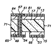
6 along the fracture channels. In Figure 10 the device includes a laminar
PTC element 17 having a first principal face to which first metal foil
electrode 13 is attached, a second principal face to which second metal
foil electrode 5 is attached, and four transverse fractured faces 71 (only
two of which are shown in Figure 10). Also attached to the second face of
the PTC element is an additional metal foil conductive member 49 which is
not rlrr~r;r~lly connected to electrode 15. Cross-conductor 51 lies within
an aperture defined by first electrode 13, PTC element 17 and additional
member 49. The cross-conductor is a hollow tube formed by a plating
process which alGo result3 in platings 52, 53 and 54 on the surfaces of the
electrode 13, the electrode 15 and the additional member 49 respectively
which were exposed during the plating process. In addition, layers of
solder 64, 65, 66 and 67 are present on (a) the first electrode 13 in the
region of the cross-conductor 51, (b) the additional member 49, (c) the
second electrode 15, and (d) the cross-conductor 51, respectively.
Figures 11-13 show other patterns of fracture channels which can be
employed to produce devices having, respectively, hexagonal, rhomboid and
T-6hape devices.
The invention is illustrated by the following Example.
E~
A conductive polymer composition was prepared by pre blending 48.6~ by
weight high density polyethylene ~Petrothene'~ Li3 832, available from USI)
. . , _ _ _ _ _ _ _ . _ . . .
W 095/34084 PCT~USg5/07420
21 923~9 ~
-12-
with 51.4% by weight carbon black (Faven'~ 430, available from Columbian
Chemicals), mixing the blend in a ~3anbury~ mixer, extruding the mixed
compound into pellets, and extruding the pellets thoug~l a 3.8 cm (1.5 inch)
extruder to produce a sheet with a thickness of 0.25 mm ~D.010 inch~. The
S extruded sheet was cut into 0.31 x 0 41 meter (12 x 16 inches) pieces and
each piece was stacked between two sheets of 0.D25 mm (0.001 inch) thick
electrodeposited nickel foil ~avaiIable ~rom Fukuda), The layers were
laminated under heat and pressure to form a pla~ue with a thickness of
about 0.25 mm (0.010 inch). the plaque was irradiated to 10 Mrad, and was
then converted into a large number of devices by the following process.
~ oles of diameter 0 25 mm (0.01 inch) were drilled through the plaque
in a regular pattern which provided one hole for each device. The holes
were cleaned, and the plan~ue was then treated so that the exposed surfaces
of the foils and of ehe holes were given an electroless copper plating and
then an electrolytic copper plating about 0.076 mm ~0.003 inch) thick.
After cleaning the plated plaque, photo resists were used to produce
masks over the plated foils except along parallel strips ~u~e~ullding to
the gaps between the additional conductive=members and the second
electrodes in the devices/ and also strips about 0.004 inch (0.1 mm) wide
~uL~uul.ding to the edges of the devices~ to be produced. The exposed
strips were etched to remove the plated foils in those areas, and the masks
removed. The etching step thus produced channels between the additional
conductive members and the second electrodes, and upper and lower fracture
channels, in the metal foils.
After cleaning the etched, plated plaque, a masking material was
screen-printed and tack-cured on one side of the plaque and then screen-
printed and tack-cured on the other side of the plaque. The screen-printed
masking material was in approximately the desired final pattern, but
somewhat oversize. The final pattern was produced by photo-curing
precisely the desired parts of the masking material through a mask,
followed by washing to remove the masking material which had not been fully
cured. On each side of the plaque, the fully cured material masked (a) the
areas corresponding to the first electrode in each device, except for a
strip rnnt~;n;ng the cross-conductor~ ~b) the etched strips, (c) the areas
W O95l34084 2 1 9 2 3 6 9 PCTrUS9~07420
.
-13- =
~LLe~ lding to the Gecond electrode, except for a strip at the end remote
from the cross-conductor, and ~d) the areas wLLe_~ullding to the additional
conductive member except for a strip adjacent to the cross-conductor.
- 5 The mask ng material was then marked ~e.g. with an electrical rating
and/or a lot number) by screen-printing an ink, followed by curing the ink,
in the areas ~LLea~llding to the first electrode ~which provides the top
surface of the installed device).
The areas of the pla~ue not covered by masking material were then
electrolytically plated with tin/lead ~63/37) solder to a thickness of
about 0.025 mm ~0 001 inch).
After the masking material and the solder had been applied, the plaque
was broken into individual devices by placing the pla~ue between two pieces
of silicon rubber, placing the resulting composite on a table, and then
rolling a roller over the composite first in one direction ~LLe~llding to
one set of fracture channels and then in a direction at right angles to the
first. The composite was then placed on the table with its other side up,
and the procedure repeated. When the composite was opened up, most of the
devices were completely separated from their neighbors, and the few which
were not completely separated could easily be separated by hand.