Note: Descriptions are shown in the official language in which they were submitted.
..
BIDIRECTIONAL VOLTAGE TRANSLATOR
Field of the Invention
The present invention relates generally to voltage translators
and, more specifically, to a voltage translator that is bidirectional.
Background of the Invention
Electronic systems employ voltage translators to interface
electronic devices that operate at different voltage levels. Such voltage
translators are sometimes bidirectional to facilitate transferring of data.
Existing bidirectional voltage translators utilize a read/write control
line to control the direction of data communication. The read/write
control line is controlled by one of the electronic devices coupled to the
bidirectional voltage translator. Due to hardware limitations, some
electronic devices are unable to accommodate the read/write control
line. Existing off-the-shelf cabling also does not accommodate the
read/write control line. What is needed, therefore, is a bidirectional
voltage translator that does not utilize a read/write control line.
It is also beneficial to implement a bidirectional voltage
translator using low cost discrete components.
Brief Description of the Drawings
2192~2G
FIG. 1 illustrates an electronic system employing a bidirectional
voltage translator;
FIG. 2 illustrates a block diagram of an embodiment of the
bidirectional voltage translator of FIG. 1;
FIG. 3 illustrates a circuit schematic of the embodiment of FIG. 2;
FIG. 4 illustrates a block diagram of an alternate embodiment of
the bidirectional voltage translator of FIG. 1;
FIG. 5 illustrates a state diagram of a process for controlling data
direction employed by the alternate embodiment of FIG. 4.; and
FIG. 6 illustrates a circuit schematic of the alternate embodiment
of FIG. 5.
Detailed Description of the Preferred Embodiments
A bidirectional voltage translator includes a first port, a second
port and a bidirectional translator circuit coupled between the first and
second ports. The first and second ports communicate signals at a first
voltage level and a second voltage level, respectively. The second
voltage level is different from the first voltage level. When a first port
signal input at the first voltage level at the first port is detected, the
bidirectional translator circuit translates the first port signal into the
second voltage level at the second port and disables translation of a
signal at the second port to the first port. When a second port signal
input at the second voltage level at the second port is detected, the
bidirectional translator circuit translates the second port signal into the
first voltage level at the first port and disables translation of a signal at
the first port to the second port. Unlike the prior art, the bidirectional
voltage translator allows two electronic devices with incompatible
2192426
_3_
voltage levels to communicate over a single bi-directional wire
without using a separate control line.
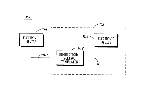
FIG. 1 illustrates electronic system 100 employing bidirectional
voltage translator 102. Electronic system 100 includes electronic device
104, wire 106, electronic device 108, and wire 110. Electronic device 104
operates at a first voltage level, such as 3 V. Wire 106 transfers signals
at the first voltage level. Electronic device 108 operates at a second
voltage level, such as 5V. Wire 110 transfers signals at the second
voltage level. Electronic device 104 is detachably coupled to
bidirectional voltage translator 102 via wire 106. Electronic device 108
is detachably coupled to bidirectional voltage translator 102 via wire
110. Bidirectional voltage translator 102 allows electronic devices 104,
108 to communicate over wires 110, 106, which form a single bi-
directional wire, without using a separate direction control line to the
translation, such as a translation read/write control line.
Electronic devices 104, 108 communicate using compatible
protocols. Such protocols allow for recovery of communication from
any data collisions. Electronic device 104 outputs communication
signals having the first voltage level on wire 106. Bidirectional voltage
translator 102 translates the voltage level of these signals to the second
voltage level and couples the translated signals to electronic device 108
via wire 110. Electronic device 108 outputs communication signals
having the second voltage level on wire 110. Bidirectional voltage
translator 102 translates the voltage level of these signals to the first
voltage level and couples the translated signals to electronic device 104
via wire 106.
Each one of electronic devices 104, 108 could be any one of a
plurality of electronic devices including, but not limited to, a cellular
radiotelephone, a cellular base station, a two-way radio, a pager, a
personal digital assistant, a computer, a modem, a Personal Computer
Memory Card International Association (PCMCIA) card, a subscriber
identity module (SIM) card, a SIM card reader, a smart card, a smart
card reader, a landline telephone, a battery charger, and the like, and
2~~2426
-4-
"device" as used herein shall refer to each of these and their
equivalents.
Field service of one of electronic devices 104, 108 can be
accomplished via electronic system 100. For example, electronic system
100 could be used to transfer cellular radiotelephone system
identification and operation data (Electronic Serial Number (ESN)
and/or Number Assignment Module (NAM) data) from electronic
device 104, which is a cellular radiotelephone that must be repaired, to
electronic device 108, which is a loaner cellular radiotelephone, via
bidirectional voltage translator 102. Electronic system 100 could be used
to program such cellular radiotelephone system identification and
operation data from electronic device 104, which is a computer or
dedicated programming box, to electronic device 108, which is a cellular
radiotelephone, via bidirectional voltage translator 102. Electronic
system 100 could also be used to test the operation of electronic device
104 by coupling electronic device 108, which could be an individual
piece or entire rack of test equipment, via bidirectional voltage
translator 102.
Bidirectional voltage translator 102, wire 110, and electronic
device 108 could be commercially packaged to provide an accessory,
such as accessory 112, that is compatible with electronic device 104. In
FIG. 1, the electronic circuitry comprising accessory 112 is illustrated as
electronic device 108 and operates at a voltage level that is different
from that of electronic device 104. Accessory 112 is detachably coupled
to electronic device 104 via wire 106. Accessory 112 could be a vehicle
accessory, such as a hands-free accessory for a cellular radiotelephone, a
data accessory, such as a modem or a PCMCIA card, or other equivalent
accessory.
Bidirectional voltage translator 102, implemented without a
separate directional control line and with only discrete components, is
illustrated in FIG. 2. Bidirectional voltage translator 102 of FIG. 2
comprises a bidirectional translator circuit including ports 200, 202,
pull-up circuits 208 - 211, and buffers 212-215.
212426
-5-
Ports 200, 202 are characterized by the voltage level of wires 106,
110, respectively. Ports 200, 202 receive signals to be translated from
wires 106, 110, respectively. Port 200 is coupled to wire 106, pull-up
circuit 208, and buffers 212, 213, 214. Port 202 is coupled to wire 110,
pull-up circuit 210, and buffers 212, 213, 215.
Buffers 212, 213 translate the voltage levels of signals at ports 200,
202. Buffers 212, 213 are unidirectional and include respective inputs
216, 218, outputs 220, 222, and enable ports 224, 226. Input 216 of buffer
212 and output 222 of buffer 213 are coupled to port 200. Output 220 of
buffer 212 and input 218 of buffer 213 are coupled to port 202. Enable
ports 224, 226 of buffers 212, 213, respectively, are coupled to buffers 214,
215.
Buffers 214, 215 control the direction of translation of buffers 212,
213. Buffers 214, 215 are unidirectional and include respective inputs
232, 234, outputs 236, 238, and enable ports 240, 242. Input 232 of buffer
214 is coupled to port 200. Input 234 of buffer 215 is coupled to port 202.
Output 236 of buffer 214 is coupled to enable port 242 of buffer 215, pull-
up circuit 209, and enable port 226 of buffer 213. Output 238 of buffer
215 is coupled to enable port 240 of buffer 214, pull-up circuit 211, and
enable port 224 of buffer 212.
Buffers 212, 213, 214, 215 are non-inverting open-drain or open-
collector buffers. Buffers 212, 213, 214, 215 are enabled to translate the
voltage levels of signals when enable ports 224, 226, 240, 242,
respectively, are pulled to a high voltage level. Buffers 212, 213, 214,
215 are disabled when enable ports 224, 226, 240, 242, respectively, are
pulled to a low voltage level.
Bidirectional voltage translator 102 is in an idle state when no
signals are present to translate at either port 200 or port 202. In the idle
state, pull-up circuits 208, 210 pull-up wires 106, 110 and ports 200, 202,
respectively, to their requisite voltage levels. If bidirectional voltage
translator 102 is a 3V to 5V translator, pull-up circuit 208 pulls up wire
106 and port 200 to 3V and pull-up circuit 210 pulls up wire 110 and
port 202 to 5V. Pull-up circuits 209, 211 enable buffers 212, 213, 214, 215
219242
_ -6-
by pulling up enable ports 224, 226, 240, 242, respectively, to the high
voltage level. ,
When a signal to be translated originates at port 200, buffer 214
turns on. Once on, buffer 214 drives both enable port 226 of buffer 213
and enable port 242 of buffer 215 to the low voltage level. This disables
buffers 213, 215 to disable communication of signals input at port 202 to
port 200. Once disabled, the voltage level of the signal is translated by
buffer 212 into the voltage level characterizing port 202 and wire 110.
The translated signal is output to port 202. By disabling buffers 213, 215
during translation from port 200 to port 202, the translated signal or
another signal at port 202 is prevented from disabling buffer 213 and/or
pulling down and latching port 200 and wire 106 through buffer 213.
When a signal to be translated originates at port 202, buffer 215
turns on. Once on, buffer 215 drives both enable port 224 of buffer 212
and enable port 240 of buffer 214 to the low voltage level. This disables
buffers 212, 214 to disable communication of signals input at port 200 to
port 202. The voltage level of the signal is then translated by buffer 213
into the voltage level characterizing port 200 and wire 106. By disabling
buffers 212, 214 during translation from port 202 to port 200, the
translated signal or another signal at port 200 is prevented from
disabling buffer 212 and/or pulling down and latching port 202 and
wire 110 through buffer 212.
If signals to be translated originate at ports 200, 202
simultaneously, all buffers 212, 213, 214, 215 will become disabled.
Buffers 212, 213, 214, 215 will remain disabled until signals at ports 200,
202 are released by their respective electronic devices 104, 108 of FIG. 1.
Aside from disabling buffers, latch-up or lock-up of bidirectional
voltage translator 102 is further avoided by fabricating buffers 212, 213
to have a larger propagation delay than the propagation delay of buffers
214, 215. Aside from fabrication, propagation delay could be increased
by coupling additional delay buffers in series with buffers 212, 213.
A circuit representation of bidirectional voltage translator 102 of
FIG. 2 is illustrated in FIG. 3. Buffers 212, 213 include transistors 300,
302 and transistors 304, 306, respectively. Buffers 214, 215 include
2192426
- transistors 308, 310, respectively. Each one of transistors 300, 302, 304,
306, 308, 310 is preferably an n-channel enhancement mode MOSFET
(metal-oxide semiconductor field effect transistor) and includes a gate, a
drain, and an intercoupled base and source that is further coupled to
electrical ground.
Transistors 300, 302, 304, 306, 308, 310 are connected as follows.
The gate of transistor 300 of buffer 212 is coupled to port 200. The drain
of transistor 300 is coupled to the gate of transistor 302 of buffer 212, the
gate of transistor 308 of buffer 214, and the drain of transistor 310 of
buffer 215. The drain of transistor 302 of buffer 212 is coupled to port
202. The gate of transistor 304 of buffer 213 is coupled to port 202. The
drain of transistor 304 is coupled to the gate of transistor 306 of buffer
213, the gate of transistor 310 of buffer 215, and the drain of transistor
308 of buffer 214. The drain of transistor 306 of buffer 213 is coupled to
port 200. The drain of transistor 308 of buffer 214 is coupled to the gate
of transistor 310 of buffer 215. The drain of transistor 310 is coupled to
the gate of transistor 308.
Pull-up circuits 208-211 include respective power supplies +Vl,
+V2, +V3, +V4 and respective resistors R1, R2, R3, R4. Pull-up circuit
208 is coupled to port 200 and the drain of transistor 306 of buffer 213.
Pull-up circuit 209 is coupled to the gates of transistors 306, 310 of
buffers 213, 215, respectively, and to the drains of transistors 304, 308 of
buffers 213, 214, respectively. Pull-up circuit 210 is coupled to port 202
and the drain of transistor 302 of buffer 212. Pull-up circuit 211 is
coupled to the gates of transistors 302, 308 of buffers 212, 214,
respectively, and to the drains of transistors 300, 310 of buffers 212, 215,
respectively. If bidirectional voltage translator 102 is a 3V to 5V
translator, suitable values for power supplies +V1, +V2, +V3, +V4 are
3V, 5V, 5V, and 5V, respectively, and a suitable value for resistors Rl,
R2, R3, R4 is 10 kS2.
In the idle state, port 200 is pulled up to voltage +Vl via pull-up
circuit 208 and the open drain of transistor 306. Similarly, port 202 is
pulled up to voltage +V3 via pull-up circuit 210 and the open drain of
219242
_ _8_
transistor 302. Buffers 212, 213, 214, 215 are effectively enabled via pull-
up circuits 209, 211 and the open drains of transistors 300, 304, 308, 310.
When translation is initiated by the signal at port 200, the
voltage at the gate of transistor 300 of buffer 212 goes to a low level.
This causes transistor 300 to turn on and the drain of transistor 300 to
go to a high voltage level. The high voltage level at the drain of
transistor 300 causes the voltage at the gates of transistors 302, 308 to
also go to a high level. In response, the drains of transistors 302, 308 are
pulled to a low voltage level. The pulling of the drain of transistor 302
to a low level translates the signal and communicates the translated
signal to port 202. The pulling of the drain of transistor 308 to a low
level disables transistors 304, 306, 310 by setting the drain of transistor
304 and the gates of transistors 306, 310 to a low voltage level. The
drains of transistors 306, 310 become open.
When translation is initiated by the signal at port 202, the
voltage at the gate of transistor 304 of buffer 213 goes to a low level.
This causes transistor 304 to turn on and the drain of transistor 304 to
go to a high voltage level. The high voltage level at the drain of
transistor 304 causes the voltage at the gates of transistors 306, 310 to
also go to a high level. In response, the drains of transistors 306, 310 are
pulled to a low voltage level. The pulling of the drain of transistor 306
to a low level translates the signal and communicates the translated
signal to port 200. The pulling of the drain of transistor 310 to a low
level disables transistors 300, 302, 308 by setting the drain of transistor
300 and the gates of transistors 302, 308 to a low voltage level. The
drains of transistors 302, 308 become open.
When translation is simultaneously initiated by signals at both
ports 200, 202, transistors 300, 304 drive transistors 308, 310, respectively,
such that the drains of transistors 308, 310 are simultaneously pulled to
the low voltage level. This causes the drains of transistors 302, 306 to
become open. Transistors 302, 306 will remain in this state until the
signals at ports 200, 202 are released by their respective electronic
devices 104, 108 of FIG. 1.
2192~2~
-9-
An alternate embodiment of bidirectional voltage translator 102,
which is also implemented without a separate directional control line,
is illustrated in FIG. 4. Bidirectional voltage translator 102 of FIG. 4
comprises a bidirectional translator circuit including ports 400, 402,
buffers 404-407, programmable logic device (PLD) 408, clock 410, and
pull-up circuits 412-415. Ports 400, 402 are characterized by the voltage
level of wires 106, 110, respectively. Ports 400, 402 receive data signals
to be translated from wires 106, 110, respectively.
Buffer 404 operates as a comparator that detects the presence of
an incoming data signal to be translated at port 400. Buffer 404 includes
input 416 and output 418. Input 416 of buffer 404 is coupled to port 400
and pull-up circuit 412. Output 418 of buffer 404 is coupled to pull-up
circuit 413 and port INl of PLD 408. When the data signal to be
translated is detected by buffer 404, a high voltage level is output to port
IN1; otherwise, a low voltage level is output to port INl.
Buffer 405 translates the voltage level of data signals originating
at port 402. Buffer 405 includes input 420 and output 422. Input 420 of
buffer 405 is coupled to port OUTl of PLD 408. Output 422 of buffer 405
is coupled to port 400 and pull-up circuit 412. Buffer 405 turns on and
translates data signals originating at port 402 into outgoing translated
data signals when port OUTl is set to a high voltage level by PLD 408.
When port OUTl is set to a low voltage level by PLD 408, buffer 405
remains off.
Buffer 406 operates as a comparator that detects the presence of
an incoming data signal to be translated at port 402. Buffer 406 includes
input 424 and output 426. Input 424 of buffer 406 is coupled to port 402
and pull-up circuit 415. Output 426 of buffer 406 is coupled to pull-up
circuit 414 and port IN2 of PLD 408. When the data signal to be
translated is detected by buffer 406, a high voltage level is output to port
IN2; otherwise, a low voltage level is output to port IN2.
Buffer 407 translates the voltage level of data signals originating
at port 400. Buffer 407 includes input 428 and output 430. Input 428 of
buffer 407 is coupled to port OUT2 of PLD 408. Output 430 of buffer 407
is coupled to port 402 and pull-up circuit 415. Buffer 407 turns on and
2192~2~
-10-
translates data signals originating at port 400 into outgoing translated
data signals when port OUT2 is set to a high voltage level by PLD 408.
When port OUT2 is set to a low voltage level by PLD 408, buffer 407
remains off.
PLD 408 controls the direction of data signal translation of
bidirectional voltage translator 102 according to a state machine 500
illustrated in FIG. 5. State machine 500 is implemented according to
software stored in the PLD 408 of FIG. 4. Each state of state machine 500
represents the direction of data signal translation. Block 502 indicates
an idle state where no data signal translation is occurring. Block 504
indicates a state where data signals received at port 400 of FIG. 4 are
translated and output to port 402 of FIG. 4. Block 506 indicates a state
where data signals received at port 402 of FIG. 4 are translated and
output to port 402. Block 508 indicates an illegal state. In the event of
reaching block 508, state machine 500 reverts to block 502.
State machine 500 operates synchronously in accordance with a
continuous train of clock pulses provided by clock 410 to PLD 408. State
evaluation and traversal occurs with the detection of each clock pulse.
States are traversed based on the voltage levels of ports IN1, IN2,
OUTl, OUT2 of PLD 408 of FIG. 4. State machine 500 remains at block
502 when ports IN1, IN2, OUTl, OUT2 are at a low voltage level,
denoted in FIG. 5 as 00/00. State machine 500 also remains at block 502
when ports IN1, IN2 are at a high voltage level and ports OUTl, OUT2
are at a low voltage level, denoted as 11 /00. State machine 500 moves
from block 502 to block 504 when port INl is at a high voltage level and
ports IN2, OUTl, OUT2 are at a low voltage level, denoted as 10/00.
State machine 500 moves from block 502 to block 506 when port IN2 is
at a high voltage level and ports IN1, OUT1, OUT2 are at a low voltage
level, denoted as 01/00.
State machine 500 remains at block 504 when ports IN1, OUT2 of
FIG. 4 are at a high voltage level and ports IN2, OUTl of FIG. 4 are at a
low voltage level, denoted in FIG. 5 as 10/01. State machine 500 also
remains at block 504 when ports INl, IN2, OUT2 are at a high voltage
level and port OUT1 is at a low voltage level, denoted as 11 /01. State
2192426
-11-
machine 500 moves from block 504 to block 502 when ports IN2, OUT2
are at a high voltage level and ports INl, OUTl are at a low voltage
level, denoted as 01/01. State machine 500 also moves from block 504
to block 502 when port OUT2 is at a high voltage level and ports INl,
IN2, OUT1 are at a low voltage level, denoted as 00/01.
State machine 500 remains at block 506 when ports IN2, OUTl of
FIG. 4 are at a high voltage level and ports INl, OUT2 of FIG. 4 are at a
low voltage level, denoted in FIG. 5 as Ol / 10. State machine 500 also
remains at block 506 when ports IN1, IN2, OUTl are at a high voltage
level and port OUT2 is at a low voltage level, denoted as 11 / 10. State
machine 500 moves from block 506 to block 502 when ports INl, OUTl
are at a high voltage level and ports IN2, OUT2 are at a low voltage
level, denoted as 10/10. State machine 500 also moves from block 506
to block 502 when port OUTl is at a high voltage level and ports IN1,
IN2, OUT2 are at a low voltage level, denoted as 00/10.
Although state machine 500 is implemented via PLD 408, it will
be recognized that state machine 500 could also be implemented using
a microprocessor or discrete components, such as flip flops.
A partial circuit representation of bidirectional voltage translator
102 of FIG. 4 is illustrated in FIG. 6. Buffers 404, 406 include
comparators 500, 502, respectively. Buffers 405, 407 include transistors
504, 506, respectively. Pull-up circuits 412-415 include respective power
supplies +V1, +V2, +V3, +V4 and respective resistors Rl, R2, R3, R4. If
bidirectional voltage translator 102 is a 3V to 5V translator, suitable
values for power supplies +V1, +V2, +V3, +V4 include 3V, 5V, 5V, and
5V, respectively, and suitable values for resistors Rl, R2, R3, R4 include
100 kS2, 10 kS2, 10 kS2, and 15 kS2, respectively. It will be recognized that
other values for resistors Rl - R4 can be used.
Comparators 500, 502 are coupled between ports 400, 402,
respectively, and PLD 408, to compare the voltage level of incoming
data signals from ports 400, 402, respectively, to a voltage level derived
from voltage references +V5, +V6, respectively. When the voltage
level of the incoming data signal at port 400 in conjunction with
resistor R6 is greater than or approximately equal to a voltage level
219226
-12-
derived from +V5, resistors R5, R7, R8, and the output voltage level of
comparator 500, comparator 500 outputs a low voltage l~yel to port IN1
of PLD 408. When the voltage level of the incoming data signal at port
402 in conjunction with resistor R10 is greater than or approximately
equal to a voltage level derived from +V6, resistors R9, R11, R12, and
the output voltage level of comparator 502, comparator 502 outputs a
low voltage level to port IN2 of PLD 408. If bidirectional voltage
translator 102 is a 3V to 5V translator, suitable values for voltage
references +V5, +V6 are 3V and 5V, respectively, and suitable values
for resistors R5, R6, R7, R8, R9, R10; R11, R12 are 10 kSZ, 10 kS2, 10 kS2,
100 kS2, 10 kS2, 10 kS2, 10 kS2, and 100 kS2, respectively. It will be
recognized that other values for resistors R5 - R12 can be used.
Transistors 504, 506, responsive to PLD 408, translate the
incoming data signals from ports 402, 400, respectively, and couple the
translated data signals to ports 400, 402, respectively. Transistors 504,
506 are open-collector bipolar junction transistors that include a base, a
collector, and an emitter. The bases of transistors 504, 506 are coupled
to ports OUTl, OUT2 of PLD 408, respectively. If an incoming signal
from port 402 is to be translated, PLD 408 outputs a high voltage signal
via port OUT2 to turn on transistor 506. Transistor 506, in conjunction
with resistors R15, R16, generates the translated voltage level of the
incoming signal at port 402. If an incoming signal from port 400 is to be
translated, PLD 408 outputs a high voltage signal via port OUTl to turn
on transistor 504. Transistor 504, in conjunction with resistors R13,
R14, generates the translated voltage level of the incoming signal at
port 402._If bidirectional voltage translator 102 is a 3V to 5V translator,
suitable values for resistors R13, R14, R15, R16 include 2.2 kS2, 10 kS2,
2.2 kS2, and 10 kS2, respectively. It will be recognized that other values
for resistors R13 - R16 can be used.
Bidirectional voltage translator 102 has been illustrated in FIGs.
1-6 as being drawn to a single wire. That is, wires 106, 110 illustrate
single bidirectional wires. It will be recognized that the above
implementations could be compatible with buses employing multiple
wires, such as the Three-Wire Bus utilized in radiotelephone products
2192~N~
-13-
manufactured and sold by Motorola, Inc. For example, the entire
embodiment of FIGs. 2 and 3 can be replicated for each additional line
of a multiple line bus. Alternatively, the buffers can be repeated and a
single buffer, such as buffer 214 of FIG. 2, can be used to control the
buffers in one direction and another single buffer, such as buffer 215 of
FIG. 2, can be used to control the buffers in the other direction. With
respect to the embodiment of FIGs. 4-6, all of the components except
the PLD and clock would be replicated for each additional line of a
multiple line bus. That is, each additional line requires four buffers,
four pull-up circuits, and a state machine.
Therefore, a bidirectional voltage translator can be implemented
that allows two electronic devices with incompatible voltage levels to
communicate over a single bi-directional wire without using a separate
directional control line. This allows the bidirectional voltage translator
to be utilized without adding additional wires to existing cabling or
additional hardware to electronic devices. The bidirectional voltage
translator can utilize a synchronous state machine or discrete
components to determine the direction of data translation based solely
on the detection of signals at ports. Once the data direction is
determined, the bidirectional voltage translator guards against latch-up
by disabling the portion of the translator not being used to translate the
data.
What is claimed is: