Note: Descriptions are shown in the official language in which they were submitted.
2192498
MICROPHONE EXPANCTfIN ~',OR BAC'K(:R(1TTNT1 Nllic~' n~nrrnmTm,.r
Field of the Inv .nr;nn
The present invention relates to the field of telephony, and in particular to
controlling background noise reduction based on the detection of an audible
voice signal
presented to a subscriber set microphone.
Background of the Invention
A problem inherent in telephony is the presence of background noise.
Generally,
the microphone of a telephone is receptive to both speech signals and to any
background
noise generated in the environment in which the microphone is located. Not
only is
background noise annoying to the caller, but the called party is also
disturbed by the effect
such background noise has on the speech signals received by the called party.
In
conference calls, each conferee is exposed to the combined background noise of
all
conferees, and therefore background noise is particularly disturbing.
The problem of background noise for the caller also effects feedback within
the
1 S subscriber set known as "sidetone". Sidetone is a small portion of the
caller's voice signal
that is fed back to the telephone's receiver to prevent the phone from
sounding "dead" to
the caller. Sidetone also allows the speaker to adjust their voice to a
desirable level. In
this manner, conversations sound normal to the caller, even though one of the
caller's ears
is blocked from receiving the caller's voice signals through the air. However,
when the
caller is not speaking, sidetone operates to feedback background noise from
the caller's
environment which can interfere with the caller's ability to hear the called
party's voice
signals. Instinctively, the caller may place his/her hand over his/her other
ear not placed
on the telephone handset to block out the background noise. This technique
does not
work because sidetone allows the background noise to be transmitted through
the receiver
of the telephone and into the caller's listening ear.
Various devices and methods have been developed to minimize or eliminate the
problems associated with background noise. In U.S. patent no. 3,691,31 l, for
example,
a telephone set is disclosed in which varying levels of attenuation (or gain)
are applied to
amplified signals received by the subscriber set's microphone. Specifically,
attenuation of
the signals is low (high gain) when a voice signal is detected, and
attenuation of the signals
2192498
-2-
is high (low gain) in the absence of a voice signal to effectively suppress
background noise
when the caller is not speaking into the microphone. Another telephone for
suppressing
background noise when the caller is not speaking is disclosed in U.S. patent
no. 5,235,637.
Another device, AT&T Corp.'s Universal Voice-Signal Conditioner chip, Part No.
LB 1068AGAW ("Conditioner"), is intended for use with commercial speaker
phones and
accommodates sidetone and suppression of background noise by varying levels of
attenuation dependent upon the strength of the microphone signal. The
Conditioner
includes a variable gain amplifier that provides different levels of gain
depending on
whether the Conditioner detects the presence of voice signals or background
noise.
In AT&T's Conditioner, a detection circuit determines whether an input signal
is
a speech signal of simply background noise. The input signals are then
provided to the
variable gain amplifier. The detection circuit sets the gain level of the
amplifier. Because
the detection circuit operates with the input signal, the detection circuit
must preamplify
the input signal to levels suitable for detection. To this end, the
Conditioner includes a
preamplifier in the detection circuit path.
The time the Conditioner takes to switch from a high gain to a low gain,
referred
to as the attack time, is fourteen milliseconds. While such relatively short
attack times are
acceptable in commercial speaker phone and other applications, it is possible
for speech
to be suppressed between syllables of speech. It should be noted that the time
it takes a
noise suppressor such as AT&T's Conditioner to switch from a low gain to a
high gain,
referred to as the decay time, is also important. If the decay time is too
long, the result is
that speech may be muted by unwanted suppression. Thus, it is desirable to
provide a
noise suppressor having attack and decay times that do not result in speech
suppression.
The telephone of U.S. patent no. 4,847,897 attempts to eliminate inadvertent
speech suppression. U.S. patent no. 4,847,897 discloses a telephone having a
noise
detector, an expander and a variable gain amplifier which provide variable
levels of
amplification depending on whether speech or mere background noise is
detected. The
noise detector distinguishes background noise from a speech signal by
examining the time-
averaged characteristics of the electrical signal emanating from the
microphone. The
expander, in response to the detection of background noise, reduces the gain
of the
219~4~~
-3-
amplifier, and, in response to the detection of a speech signal, increases the
gain of the
amplifier.- More specifically, the telephone of U.S. patent no. 4,847,897
attempts to avoid
speech suppression by providing circuitry to compare a short-term average
(approximately
fifty milliseconds) of the microphone signal to a long-term average
(approximately four
seconds) of the microphone signal, as it is assumed that speech is usually not
continuous
for more than four seconds, and breaks in speech usually do not exceed fifty
milliseconds.
However, like AT&T's Conditioner, noise detection is performed using the
microphone
signal, before the signal is passed through the variable gain amplifier. Also,
the time-
averaging technique introduces additional cost to the telephone in addition to
expending
time in performing the averaging. Therefore, it is desirable to provide a
noise suppressor
that is inexpensive to manufacture and whose suppression method is efficient
and simple
to perform.
It is also desired that a noise suppression apparatus be configurable to be
able to
be used in a variety of environments. For example, the apparatus should be
able to
suppress noise for commercial telephones, such as commercial speakerphones, in
which
the background noise may be particularly annoying to the called party. The
apparatus
should also be applicable for residential telephones, both traditional
telephones, and
cordless phones. Further, it is desired that the noise suppression apparatus
be useful for
cellular telephones.
Summ__ary of Ln_vention
The present invention provides a microphone expander that provides a gain
adjustment depending upon whether voice signals are present. In particular,
signals are
amplified by a high gain level or a low gain level depending upon the level of
a detected
microphone signal. The microphone signal is detected after the gain adjustment
has
occurred, thereby reducing the circuit components required and further
providing a
hysteresis effect.
A preferred embodiment of the present invention is an apparatus for reducing
background noise in a telecommunications device, the telecommunications device
including a microphone that receives both voice signals and background noise
signals. The
CA 02192498 1999-08-OS
-4-
microphone is further operable to converting the voice signals and background
noise signals
into electrical signals. The apparatus includes an amplifier having an input
for receiving the
electrical signals and an output, said amplifier operable to receive
electrical signals at the
input and provide amplification to the electrical signals to produce amplified
electrical
signals. The amplifier is further operable to provide amplification at a first
gain level and a
second gain level, wherein the first gain level exceeds the second gain level.
The apparatus
also includes a feedback device connected to the output of the amplifier and
further operably
connected to control the operation of the amplifier. The feedback device is
operable to cause
the amplifier to provide amplification at the first gain level when the
feedback device receives
amplified electrical signals at the output having an amplitude above a
predetermined threshold
and cause the amplifier to provide amplification at the second gain level when
the feedback
device receives amplified electrical signals at the output having an amplitude
below a
predetermined threshold.
In accordance with one aspect of the present invention there is provided an
apparatus
for reducing background noise in a telecommunications device, the
telecommunications
device including a microphone for receiving acoustic signals, the acoustic
signals including
voice signals and background noise signals, the microphone being further
operable to convert
the acoustic signals into corresponding electrical signals, the apparatus
comprising: a) an
amplifier having an input for receiving the electrical signals and an output,
said amplifier
operable to receive the corresponding electrical signals from the microphone
at said input and
provide amplification of the corresponding electrical signals to produce
amplified electrical
signals at the output, said amplifier operable to provide amplification at a
first gain level and
a second gain level, said first gain level exceeding the second gain level;
and b) a feedback
device connected to the output of the amplifier and further operably connected
to control the
operation of the amplifier, the feedback device operable to cause the
amplifier to provide
amplification at the first gain level when the feedback device receives
amplified electrical
signals at the output having an amplitude above a predetermined threshold and
cause the
amplifier to provide amplification at the second gain level when the feedback
device receives
amplified electrical signals at the output having an amplitude below the
predetermined
threshold.
CA 02192498 1999-08-OS
-4a-
In accordance with another aspect of the present invention there is provided a
method
of controlling the amplification of electrical signals in a telecommunication
device having a
microphone, the method comprising: a) providing electrical signals from the
microphone to
an amplifier; b) employing the amplifier to amplify the electrical signals
using one of at least
two gain levels, the at least two gain levels including a high gain level and
a low gain level;
c) providing the amplified electrical signals to a feedback device; d)
employing the feedback
device to determine a relationship between an amplitude of the amplified
electrical signals and
a predetermined threshold; and e) causing the amplifier to amplify subsequent
signals using
the high gain level if the amplitude of the amplified electrical signals
exceeds the
predetermined threshold.
The above discussed features, as well as additional features and advantages of
the
present invention, will become more readily apparent by reference to the
following detailed
description and the accompanying drawings.
Brief Description of the Drawings
Fig. 1 illustrates a block diagram of an exemplary embodiment of a handset of
a
telephone according to the present invention;
Fig. 2 illustrates a schematic block diagram of an exemplary embodiment of the
microphone expander according to the present invention;
Fig. 3 illustrates a gain relationship of an operational amplifier used in the
exemplary
microphone expander circuit of Fig. 2; and
Fig. 4 illustrates in further detail a schematic diagram of the exemplary
microphone
expander of Fig. 2.
Detailed Description
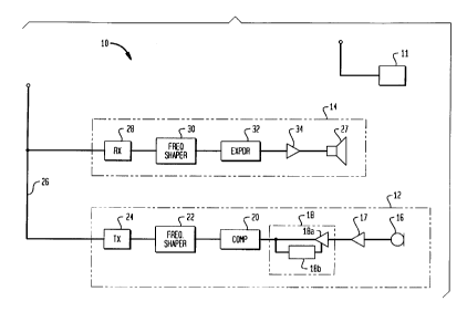
Fig. 1 shows a block diagram of an exemplary embodiment of a telephone
handset 10 according to the present invention. In this embodiment, the
telephone handset 10
2I924~8
-5-
comprises a cordless telephone handset for use with a telephone base unit 11
and is
functionally divided into a microphone portion 12 and a receiver portion 14.
The
telephone handset 10 includes a conventional microphone 16 for receiving
acoustic signals
from the caller and any background noise located in the environment, and
producing
electrical signals therefrom. The electrical signals from the microphone 16
are amplified
by an audio amplifier 17 and then provided to a microphone expander 18. The
handset 10
is designed to operate in conjunction with the base unit 1 l, which
communicates with the
handset 10 via radio frequency or RF signals. The base unit 11 is further
connected to a
telecommunication network, not shown.
In general, the microphone expander 18 includes an amplifier 18a and a
feedback
device 18b. The amplifier 18a is a variable gain amplifier that has an input
for receiving
the electrical signals and an output connected to the compressor 20. The
amplifier 18a
according to the present invention is operable to receive electrical signals
and provide
amplification to the received electrical signals at a first gain level and a
second gain level,
the first gain level exceeding the second gain level. The feedback device 18b
is connected
to the output of the amplifier and further operably connected to control the
operation of
the amplifier 18a. Specifically, the feedback device 18b causes the amplifier
18a to
provide amplification at the first gain level when the feedback device 18b
receives
amplified electrical signals at the output having an amplitude substantially
above a
predetermined threshold. Likewise, the feedback device 18b causes the
amplifier 18a to
provide amplification at the second gain level when the feedback device
receives amplified
electrical signals at the output having an amplitude substantially below the
predetermined
threshold. In a preferred embodiment, discussed in detail below in connection
with Figs 2
and 3, the feedback device 18b is further operable to cause the amplifier to
provide
amplification at a third gain level when the feedback device 18b receives
amplified
electrical signals at the output having an amplitude approximately equivalent
to the
predetermined threshold.
The amplified electrical signal generated by the microphone expander 18 is
then
compressed and shaped by a compressor 20 and a frequency shaper 22,
respectively, by
means and apparatus well known in the art. The compressed, shaped signal is
then
2192498
-6-
transmitted from the microphone portion 12 of the handset 10 to the base unit
11 by an
RF transmitter 24. The base unit as well known in the art, typically includes
an RF
receiver, RF transmitter, frequency shaper) audio amplifier and hybrid
circuit. The base
unit 11 provides the transmitted signal to the telecommunication network,
which in turn
provides the signal to another telephone, not shown.
The base unit 11 further receives signals from other telephones through the
telecommunication network. These signals are transmitted to the receiver
portion 14 of
the handset 10. The receiver portion 14 is comprised of components well known
in the
art. specifically, the receiver portion 14 of the handset 10 includes an
antenna 26 and an
RF receiver 28 for receipt of the RF signals generated by the base unit 1 1.
The received
signal is then shaped and expanded by a frequency shaper 30 and an expander
32,
respectively. The shaped and expanded signal in the receiver portion 14 is
then provided
through an audio amplifier 34 to an earpiece 17 for presentation of audio
signals to the
caller.
In addition, the caller is able to hear his/her own voice generated by the
microphone 16 through sidetone coupling. Signals generated by the caller at
the
microphone portion 12 are provided to the base unit 11 through the RF
transmitter 24 as
described above. Circuitry within the base unit 11 couples and transmits a
portion of the
transmitted signal back to the receiver portion 14, providing sidetone.
Referring now to Fig. 2, there is illustrated a partial schematic diagram of
an
exemplary embodiment of the microphone expander 18 according to the present
invention.
The basic elements of the amplifier 18a include resistors RA, RB and RF and an
operational amplifier ("op-amp") 44. The feedback device 18b further includes
a trigger
circuit 40, a low pass filter, and a rectifier 42. The microphone expander 18
also includes
an input IN and an output OIJT. The op-amp 44 has first and second input
stages 45 and
46, respectively, and a common output stage 47. In general, the expander 18 is
designed
to provide background noise reduction during periods of silence, i.e., when
the caller is not
speaking into the microphone.
The low pass filter comprises a resistor 51 and a capacitor 52 and is
connected
between the rectifier 42 and the trigger circuit 40. The trigger circuit 40 in
the exemplary
2192498
_7_
embodiment includes two bipolar junction transistors in differential pair
configuration
( "differential pair"). The trigger circuit 40 is connected to a reference
voltage, VHF at
input 54 and is operably connected to the op-amp 44 to controllably switch
between
activation of the first input stage 45 and the second input stage 46 in the
manner as will
be more fully described below. In other words, the trigger circuit 40 is
operably connected
to control the gain applied by the microphone expander 18.
The first and second input stages 45 and 46 are each in inverting
configuration,
sharing the same output stage 47. A feedback resistor RF connects the output
OUT to an
inverting input IN1 of the first input stage 45. The inverting input IN 1 of
the first input
stage 45 is also connected to a resistor RB, which is in turn connected to the
input IN
through another serially-connect resistor RA. There is also a line connection
49 between
the intersection of the resistors RA and RB and an inverting input IN2 of the
second input
stage 46. So connected, a first feedback path is defined in this embodiment by
RF, and a
second feedback path is defined in this embodiment by RF and RB. The gain from
the
input IN to the output OUT is determined by the ratio of the effective
feedback resistance
of the feedback path divided by the effective input resistance. Depending on
which input
stage 45 or 46 is selected by the trigger circuit 40, the gain is set
according to the
following relationships:
For Low Gain: G = RF / (RA + RB)
For High Gain: G = (RF + RB) / RA
where VouT = V~ G.
In operation, the microphone expander 18 receives electrical input signals V~,
consisting of electrical voice signals from the microphone circuitry at the
input IN and
produces output signals VouT consisting of amplified electrical signals at the
output OUT.
To produce the amplified electrical signals, the microphone expander VouT
amplifies V~
by one of two gain levels, a high gain level or a.low gain level. The
selection of which gain
level is applied is accomplished by the trigger circuit 40, which selectively
activates one
of the two input stages 45 and 46, or some combination thereof. The op-amp 44
provides
2192498
.g_
a low gain level when the first input stage 45 is inactive and the second
input stage 46 is
active, and provides a high gain level when the first input stage 45 is active
and the second
input stage 46 is inactive. In general, the microphone expander 18 provides a
high gain
level when it detects output signals VouT at its output that exceed a
predetermined
threshold, which is indicative of active speech or conversation. By contrast,
the expander
18 provides a low gain level when it detects output signals VouT below the
threshold,
which is indicative of no speech, or in other words, a pause in a
conversation.
The input signals VIN are provided to each of the input stages 45 and 46 at
inputs
IN 1 and IN2, respectively. A suitable bias signal V~oM is applied to the
noninverting
inputs of each of the input stages 45 and 46. The op-amp 44 provides at its
output OUT
the voice signal amplified by the gain level associated with whichever of the
input stages
45 and 46 that is active. According to this embodiment, the high gain level is
6dB and the
low gain level is OdB. The 6dB difference between the high and low gain
provides for
smoother sounding transitions than is possible with larger gain differences.
In particular,
if the gain difference is much larger, for example, 20dB, the transitions
between high and
low gain may be more noticeable. Moreover, the use of a large gain difference
may make
it more difficult to differentiate active conversation from noise at the op-
amp output OUT.
Nevertheless, if the expander 18 is implemented in a speaker phone, a 20dB
gain difference
may be more appropriate to achieve a high suppression level.
The amplified electrical signal VouT at the output OUT is provided as feedback
through the rectifier 42, which in the present embodiment is a half-wave
rectifier. The low
pass filter then smooths the rectified signal to provide a substantially do
voltage level VR",,s
that is indicative of the amplitude level of signal VouT provided at the
output OUT. The
do voltage level Vas is applied to the input 53 of the trigger circuit 40
which compares
this signal to a reference voltage level VHF. In the exemplary embodiment, the
half-wave
rectifier provides an inverted rectified output, and thus, Vas is lower (more
negative) for
higher amplitude VouT signals. As a result, if Vas is substantially lower than
VHF, then
Vouz. has an amplitude greater than the predetermined threshold and, as a
result, the trigger
circuit 40 provides a signal on line 56 that causes the first input ~ :~e 45
to be active. If,
however, VRMS is substantially greater than VHF, then the trigger circuit 40
provides a
219498
-9-
signal to the input 56 of op-amp 44 that causes the first input stage 45 to be
inactive and
the second input stage 46 to be active. If the level of V,~S is somewhat close
to the level
Of VREF, then the trigger circuit 40 causes a combination of the first and
second input
stages 45 and 46 to be active, which effectively provides a gain level in
between the high
and low gain levels. In particular, when both the first and second input
stages 45 and 46
are active, a portion of V~, receives low gain amplification and a portion of
VIN receives
high gain amplification, thereby providing an overall gain level between the
high and low
gain level.
The choice of appropriate V~ and VooM voltage levels will necessarily depend
on
the particular implementation, including the measured amplitude of output
signals for both
active speech and background noise input signals. Those of ordinary skill in
the art can
readily determine the appropriate levels for their implementation.
It should be noted that the use of an inverting rectifier as the rectifier 42
is given
by way of example only. Those of ordinary skill in the art may readily employ
a
noninverting rectifier in which case the trigger circuit 40 would be
configured to activate
the first input stage 45 when V,u,,ts is greater than VHF.
Fig. 3 shows the gain of the op-amp 44 as a factor of the difference between
VAS
and V~... The curve between the point at which VAS « VHF and VAS » V,~F allows
for a smoother transition between the low and high gain levels. The smooth
transition
causes less abrupt gain switching that could otherwise cause a telephone
conversation to
sound choppy. The response shown in Fig. 3 is caused primarily by the output
response
of the trigger circuit 40 of Fig. 2. The trigger circuit 40 according to an
exemplary
embodiment described further below in connection with Fig. 4, comprises two
bipolar
junction transistors commonly connected at their respective emitters. The
nature of the
response of bipolar junction transistor differential pair typically has the
shape illustrated
in Fig. 3. In an alternative embodiment, the trigger circuit 40 may suitably
have a step
response if a smooth transition is not required by the application.
Another advantage of the present invention, not illustrated in Fig. 3, is the
hysteresis created by measuring the microphone signal strength at the output
of the
expander amplifier 18a. Consider a situation in which large amplituded signals
indicative
292498
- 10-
of active conversation are being provided to the input IN and the amplifier is
providing
high gain. Small downward fluctuations or slight reductions in signal strength
do not
cause activation of the second input stage 46 (and reduce gain) because the
slightly
reduced signal receives high gain, which maintains Vour at a high level such
that VAS is
sufficiently lower than VHF. If a true low amplitude signal is applied to IN,
then VAS
does rise above VHF and the expander 18 activates the second input stage 46.
The
hysteresis thus provides improved operation by reducing the number of
inadvertent or
undesirable transitions between the high and low gain levels.
Also important to any background noise suppression are the attack and decay
times
for application of noise suppression. In the embodiment of FIGS. 2 and 3, both
the decay
and attack times are 100 microseconds. The attack and decay times are
determined by the
time constant of the low pass filter created by the resistor 51 and the
capacitor 52. The
preferred attack and decay times were determined experimentally using human
subjects
and obtaining their subjective judgment on the application of various times.
It should be
noted that the microphone expander 18 of the present invention has attack and
decay times
that are significantly less than that of the prior art. For example, AT&T's
Conditioner,
previously described herein, has an attack time of 14 milliseconds and a decay
time of 140
milliseconds. Thus, the resolution of the present invention is much finer than
that of the
prior art, likely resulting in many more occurrences of background noise
suppression in a
given speech pattern than in the prior art. The quick responsiveness results
in fewer
instances of unwanted speech suppression.
Fig. 4 shows in further detail a first embodiment of the microphone expander
18
operating according to the present invention. Where appropriate, reference
numbers used
in Fig. 2 will also be used to identify the corresponding circuit elements in
Fig. 4. Unless
otherwise specified, any transistors referenced herebelow are bipolar junction
transistors,
each which having a base, collector and emitter as is known in the art. The
elements
shown in Fig. 4 may suitably be integrated onto single semiconductor
substrate. In an
alternative embodiment, however, the feedback resistors RA, RB and RF are not
integrated onto the substrate, but rather are externally connected in order to
allow gain
level adjustment by circuit designers.
.~ 21924~~
-11-
In addition to the circuit elements described below) the expander 18 also
includes
voltage bias points CC, FF (ground), COM, and BA, signal points IN 1) IN2,
RCT, Rl'~IS,
and REF. The expander 18 as illustrated in Fig. 4 also includes first and
second current
mirrors 53 and 54. In a semiconductor implementation of the expander, the bias
point
voltages are all externally provided directly or indirectly through, for
example, pin
connections. In the following description, the voltage of any bias point or
signal point is
represented as Vx wherein x is the reference used to identify the bias point
or signal point.
For example, V~oM represents the voltage at the point COM.
The trigger circuit 40 comprises transistors Q 1 and Q2 commonly connected at
their respective emitters. The trigger circuit 40 further includes another
transistor Q4, the
collector of which is connected to emitters of the transistors Q 1 and Q2. The
emitter of
Q4 is connected to ground. The base of the transistor Q 1 is connected to the
point REF.
The point REF is connected to COM through R1, and to FF (ground) through a
transistor Q3 and serially connected resistors R2A and R2B. The base of the
transistor Q3
is connected to the reference voltage point BA. So connected, the voltage VBA
forward
biases the transistor Q3, and the resulting voltage drop through the emitter
of the
transistor Q3 and the resistors R 1 A and R2A sets the current level through
the collector-
emitter junction of the transistor Q3. This current level defines the current
through the
resistor Rl, which thereby defines the voltage drop across R1. Accordingly,
VHF, which
is equal to VcoM minus the drop over the resistor R1, may be set by altering
the value of
the resistance R 1. For example, by increasing the resistance of R 1, the
voltage drop across
R1 increases, and thus VHF decreases.
In the present embodiment the resistors R1, R2A and R2B are each 25k ohms. In
addition, the voltage drop from the base to emitter of the transistor Q3 is
approximately
.75 volts. Moreover, V~oM is approximately 1.8 volts and VBA is approximately
1.0 volt,
all of which are provided externally. In this embodiment, then, the current
through R2A
and R2B, and likewise through R 1 is approximately 5 microamps. As a result,
VHF is
equal to 1.8 - (5 X 10'6)(25k) or 1.675 volts.
The output of the trigger circuit 40 is the combination of the collectors of
the
transistors Q 1 and Q2. One part of the output, the collector of the
transistor Q 1 is
2192498
-12-
connected to the first current mirror 53. The other part of the output, the
collector of the
transistor Q2, is connected to the second current mirror 54. The first current
mirror S3
is there after connected to the first input stage 45, and the second current
mirror 54 is
further connected to the second input stage 46.
In further detail, the first current mirror 53 consists of two PNP transistors
QS and
Q 12, the emitters of which are connected to CC, and the bases of which are
connected to
each other. The collector of the transistor QS is connected to the
differential pair output,
and in particular, the collector of the. transistor Q 1. The base and
collector of the
transistor QS are further connected to each other. The second current mirror
54 also
consists of two PNP transistors Q6 and Q7, the emitters of which are also
connected to
the bias point CC and the bases of which are connected to each other. The base
and
collector of the transistor Q6 are further connected to each other. In
addition, the
collector of the transistor Q4 is connected to the output of the trigger
circuit 40, and in
particular, to the collector of the transistor Q2.
The first input stage 54 consists of two transistors Q 10 and Q 11 connected
in
differential pair form, with one differential pair input, the base of the
transistor Q 10,
forming the non-inverting input and the other differential pair input, the
base of the
transistor Q11, forming the inverting input. The non-inverting input is
connected to COM
and the inverting input is connected to IN1. The second input stage 46
includes two
transistors Q8 and Q9 configured in an analogous manner as the first input
stage 45,
except that the inverting input of the second input stage is connected to IN2.
The first and
second input stages 45 and 46 each have outputs connected to the op-amp output
stage
47.
The rectifier 42 in the present embodiment has the following structure. The
rectifier includes a differential pair of PNP transistors QR2 and QR3, the
emitters of which
are connected to each other. The base of the transistor QR2 is connected to
OUT through
a resistor RR1. The base of QR3 is connected to COM through a resistor RR4,
and RCT
through a resistor RR3. The collectors of QR2 and QR3 are each connected to an
input
of a current mirror consisting of two NPN transistors QR4 and QRS. The
collector of the
transistor QR2 is further connected to the base of an NPN transistor QX. The
emitter of
2192498
- 13-
the transistor QX is connected to ground FF and the collector of the
transistor QX is
connected to the anode of zener diode Z 1. A capacitor CCR is also connected
between
the base and collector of the transistor QX. The cathode of the zener diode Z
1 is
connected to RCT. The emitters of QR2 and QR3 are connected to each other and
to an
emitter of a biasing transistor QR1.
In a preferred embodiment of the present invention, the resistor RR 1 is an
8.6k
ohm resistor, the resistor RR3 is a 45k ohm resistor, and the resistor RR4 is
a lOk ohm
resistor. The capacitor CCR is a 2pf capacitor.
In operation, the rectifier 42 receives the output signal VouT of the op-amp,
and
produces a rectified version thereof at its output, which is the point VR~..
The rectified
output signal in this embodiment consists essentially of the negative cycles
of VouT. The
low pass filter then smooths the negative cycles into a more or less do
voltage level that
represents an average, or more specifically, root-mean-square of the negative
cycles of
Vocrr. This root-mean-square voltage, VAS, is then provided to one input of
the trigger
circuit 40. Then as described above, the trigger circuit 40 activates either
the first input
stage 45, the second input stage 46, or some fraction of both depending on the
difference
between VAS and VREF.
In further detail, consider a large output signal VouT, which corresponds to
active
speech. The large output signal will include large negative swings in voltage
in the
negative cycles. During these negative swings, QR2 tends to turn on to a
greater extent
than QR3. As a result, emitter-collector current through QR2 will tend to turn
on the
transistor QX. Because QX is turned on, large amounts of current pass through
the zener
diode Z1, and the voltage VR~.I. is drawn low. Specifically, the current
through the zener
diode Z1 causes a large voltage drop from COM through the resistors RR3 and
RR4, and
as a result VR~ is relatively low compared to VooM. The low voltage VR~. is
then passed
through the low pass filter, which produces a low VAS relative to VooM.
Because VHF
is slightly less than VooM, as discussed above, the low VAS at the base of Q2
will tend to
turn off the transistor Q2 and turn on the transistor Q 1. Under these
conditions, the
transistor Q 1 causes current to flow through the transistor QS and thus
through the
transistor Q 12. The current through the transistor Q 12 provides a bias
current to the
2192498
- 14-
emitters of the transistors Q 10 and Q 11 which activates the differential
input of the first
input stage 45. The transistor Q2, however, allows little or no current to
flow from the
collector of Q6, which tends to turn off both transistors Q6 and Q7. Because
the
transistor Q7 is turned off, no current flows to the emitters of the
transistors Q7 and Q8,
which deactivates the input stage 46.
As a result, large signals at the output VoUT having large negative voltage
swings
tend to activate the first input stage 45. When the first input stage 45 is
activated, the
input V~1 applied to the inverting input IN1 provides the high gain level, as
determined
by the resistor RA, RB and RF of Fig. 2. Accordingly, large signals typically
associated
with active conversation, as opposed to background noise, cause the expander
18 to
provide a high gain level from input to output.
In the case of smaller signals at the output OUT, such as may be present when
only
background noise in present, the transistor QR2 tends to turn on to a lesser
extent.
Accordingly, the transistor QR3 tends to turn on to a greater extent, which,
in turn, causes
the current mirror defined by the transistors QR4 and QRS to pull the voltage
at the base
of the transistor QX low. Under these conditions, the transistor QX will tend
to turn off,
or at least, conduct current to a lesser extent. As a result, less current is
provided through
the zener diode Z1 and the voltage VRC.i. tends to elevate towards VcoM. The
relatively
high VR~. voltage passes through the low pass filter and provides a voltage
VAS which
approaches the level of VcoM. Because VAS is close to VcoM and VHF is slightly
less than
VcoM, the voltage V,~S tends to turn on the transistor Q2 and tends to cause
the transistor
Q 1 to turn off. The transistor Q2 allows current to flow from the current
mirror 54 which
in turn activates the second input stage 46. The transistor Q1, however,
allows little or
no current to flow from the current mirror 53, which in turn deactivates the
first input
stage 45. The second input stage 46, as discussed above in connection with
Fig. 2,
provides a low gain from the input IN2 to the output OUT because of the
configuration
of the resistors RA, RB and RF of Fig. 2.
It may be preferable to replace the exemplary rectifier circuit 42 and the low
pass
filter as configured with an alternative means for converting the output
signals to a do
voltage level. In particular, a full wave rectifier having a current output
summed to a
2192498
- 15-
parallel resistor-capacitor circuit may be used instead of the exemplary
rectifier 42 and low
pass filter illustrated in Fig. 4. An example of a suitable full wave
rectifier may be found
in many commercially available compander (combined compressor and expander)
integrated circuits, such as those manufactured by Motorola and Signetics.
Although the embodiment of Fig. 1 comprises a residential cordless telephone
set,
it will be appreciated by those of skill in the art that the microphone
expander and
background noise suppression method of present invention may be used in any
telephone
set, whether its primary use is intended as residential or commercial. Those
of ordinary
skill in the art may readily determine the appropriate levels of attenuation
and the attack
and decay times appropriate for the particular telephone and its intended
environment.
Once such appropriate levels are determined, the circuit may readily be
modified as
appropriate.
It will also be appreciated that the microphone expander 18 need not reside in
the
telephone handset as illustrated in Fig. 1. Although such placement may be
preferable for
cordless telephones so that the raw microphone signal does not need to be
transmitted to
the telephone base, there is no requirement that the microphone expander
reside in the
handset. Further, for telephones having the majority of its electronics
located in the base,
such as a traditional corded telephone, it is preferable to place the
microphone expander
18 in the telephone base. Similarly, all electronics, including the microphone
may exist in
the telephone handset, such as in a cellular telephone.
It will be further appreciated that the microphone expander of the present
invention
is inexpensive to manufacture and operates in an efficient manner. Because
noise
suppression is determined at the output of the expander, no preamplifier is
required
between the audio amplifier connected to the microphone and the expander, as
is required
in the prior art. The elimination of the preamplifier not only reduces the
cost of the device,
but also eliminates a redundant function, as preampliftcation also occurs
within the
expanders of the prior art. Further, the response of the device is very
efficient as it does
not require time averaging of signals received by the microphone.
It will be appreciated that the above embodiments are merely illustrative and
that
those of ordinary skill in the art may readily envision or develop other
embodiments that
2192498
- 16-
incorporate the principles of the present invention and fall within the scope
and spirit
thereof.