Note: Descriptions are shown in the official language in which they were submitted.
2 ~ 9 3 G 1 2
~ SURFACE ACOUSTIC WAVE APPARATUS
BACKGROUND OF THE INVENTION
The present invention relates to a surface acoustic wave apparatus using a
l~min~ted ceramic substrate as a packaging member, and more particularly, to a
surface acoustic wave apparatus in which a phase unit is disposed within a l~min~ted
ceramic substrate.
Surface acoustic wave devices have been widely used in various fields such
as the mobile communication field. In an actual component which includes a surface
acoustic wave device, the device is accommodated in a hermetically sealed case made
of metal or a package using a l~min~ted ceramic substrate.
As electronic units have become more compact, it is required that circuits or
apparatuses using surface acoustic wave devices also become more compact. In a
mixed integrated circuit including a surface acoustic wave device and a semiconductor
device, an attempt has been made to reduce the size of the circuit by using a
multi-layer circuit substrate as a packaging member, as in Japanese Utility Model
Application No. 2-8145.
The foregoing utility model application discloses a mixed integrated circuit in
which a multi-layer circuit substrate provided with an electronic circuit disposed
therein is used as a packaging member for packaging either a semiconductor device
or a surface acoustic wave device or both, and the semiconductor or surface acoustic
wave device is electrically connected to the electronic circuit.
~193012
Since the mixed integrated circuit uses the multi-layer circuit substrate
including the electronic circuit as a packaging member, what was conventionally only
a packaging member now contains the electronic circuit with electronic devices such
as resistors and capacitors. Therefore, an electronic unit with such a mixed
integrated circuit can presumably be constructed to be compact and lightweight.
A l~min~ted ceramic substrate used as a packaging member in a surface
acoustic wave device is made from an insulating Al2O3 ceramic to achieve reliability
and low cost.
In some cases, when impedance matching is required, a phase unit is disposed
at the input and output ends of a surface acoustic wave device. In this case, animpedance-matching phase unit is conventionally connected to an exterior surface of
a surface acoustic wave apparatus which contains a surface acoustic wave device
therein.
When a phase unit is disposed in a l~min~ted ceramic substrate serving as a
packaging member constituting a surface acoustic wave apparatus, the apparatus can
be made compact. However, the inventors of the present application have discovered
that the thickness of the surface acoustic wave apparatus increases and the
characteristics of the apparatus deteriorate when the phase unit is disposed within the
l~min7~ted ceramic substrate in the apparatus.
When a phase unit is disposed in a ceramic substrate with a signal line and
ground electrodes being formed separately between different ceramic layers, the
characteristic impedance of the phase unit is determined by the dielectric constant of
the ceramic used, the width of the signal line, and the distances between the signal
line and the ground electrodes. The l~min~ted ceramic substrate serving as a
~1 93~1~
packaging member in the surface acoustic wave apparatus is usually made from high
purity alumina and its relative dielectric constant is about 10.
When a phase unit is disposed in a ceramic substrate made from alumina
having a relative dielectric constant as high as about 10, the thickness of a section
corresponding to the phase unit increases and a line length corresponding to the delay
time is required. Therefore, when a phase unit is disposed in a l~min~ted ceramic
substrate made from the above-described alumina, the substrate is thicker than when
the l~min~ted ceramic substrate serves just as a packaging member in a surface
acoustic wave device, and the surface acoustic wave apparatus is prevented from
having a low profile.
To make the l~min~ted ceramic substrate thinner, the width of the signal line
in the phase unit needs to be reduced. In this case, the resistance of the signal line
increases and a large insertion loss occurs. As a result, the characteristics of the
surface acoustic wave apparatus deteriorate.
The preferred embodiments of the present invention overcome the problems
described above by providing a surface acoustic wave apparatus including a packaging
member comprising a l~min~ted ceramic substrate, the apparatus being adapted to
suppress an increase in insertion loss of a phase unit, and to reduce the height of the
apparatus, even if the phase unit is disposed within the l~min~ted ceramic substrate.
A preferred embodiment of the present invention provides a surface acoustic
wave apparatus including a l~min~ted ceramic substrate preferably made from a
dielectric ceramic having a relative dielectric constant of about 7 or less; a phase unit
2l93ol2
disposed within the l~min~te~ ceramic substrate; and a surface acoustic wave device
disposed on the l~min~ted ceramic substrate and electrically connected to the phase
unit.
The surface acoustic wave apparatus of the preferred embodiments of the
S present invention has a phase unit disposed within the l~min~ted ceramic substrate on
which the surface acoustic wave device is mounted. The l~min~ted ceramic substrate
serves as part of a packaging member for the surface acoustic wave apparatus. Since
the phase unit is built within the l~min~ted ceramic substrate which functions as a
packaging member, the surface acoustic wave apparatus has a compact construction.
In addition, since the l~min~ted ceramic substrate is made from a dielectric
ceramic having a relative dielectric constant of about 7 or less, a portion constituting
the phase unit can be made thinner than in a l~min~ted ceramic substrate made from
alumina, and an increase in insertion loss is prevented.
The surface acoustic wave a~a~ s of the preferred embodiments of the
present invention may be configured such that the phase unit includes a signal line
disposed within the l~min~ted ceramic substrate and first and second ground
electrodes disposed above and below a respective one of the signal lines, within the
l~min~ted ceramic substrate, and the area of the ground electrodes are larger than the
area of the signal line. In the phase unit having the structure described above, since
the l~min~ted ceramic substrate is made from a dielectric ceramic having a relative
dielectric constant of about 7 or less, the distance between the upper and lowerground electrodes can be made shorter while the width of the signal line is maintained
as is when compared with a l~min~ted ceramic substrate made from alumina.
Therefore, an increase in insertion loss in the surface acoustic wave apparatus is
2193()12
- suppressed and the entire surface acoustic wave apparatus has a substantially reduced
height.
Since the l~min~ted ceramic substrate serving as part of a packaging member
is made from a dielectric ceramic having a relative dielectric constant of about 7 or
S less and a phase unit is built within the l~min~ted ceramic substrate in the surface
acoustic wave apparatus of the preferred embodiments of the present invention, an
increase in insertion loss is avoided and the package has a substantially reduced
height.
The surface acoustic wave apparatus may be configured such that the phase
unit is formed at two locations within the l~min~ted ceramic substrate, signal lines for
the two phase units are located at different heights, and a second ground electrode of
the upper phase unit and a first ground electrode of the lower phase unit are formed
as a common ground electrode, and the distance between the ground electrodes of one
phase unit differs from the distance between the ground electrodes of the other phase
unit.
Since the ground electrode disposed between the signal lines of the two phase
units is used as a common ground electrode, the number of ground electrodes is
reduced, thereby the cost is reduced and the package is further reduced in height.
When the width of a signal line is reduced to a minimum amount, which is specified
by machining precision, a portion constituting the two phase units in a case in which
the two phase units have different characteristic impedances and are formed in the
direction of l~min~tion can be made to have a minimum height by varying the
distances between the ground electrodes of the two phase units.
2193~)12
In the preferred embodiments of the present invention, the l~min~te~ ceramic
substrate is preferably made from a dielectric ceramic having a relative dielectric
constant of about 7 or less. The dielectric ceramic is not limited to any particular
types. It is preferred that the l~min~ted ceramic substrate be made from a
BaO-SiO2-Al2O3 dielectric material disclosed in the Japanese Examined Patent
Publication 6-76253. In other words, the BaO-SiO2-Al2O3 dielectric m~teri~l
preferably includes about 25 to about 80 weight percentage of the Si component in
terms of SiO2, about 15 to about 70 weight percentage of the Ba component in terms
of BaO, about 1.5 to about 5 weight percentage of the B component in terms B2O3,about 1 to about 30 weight percentage of the Al component in terms of Al2O3, andmore than about 0 to about 30 weight percentage of the Ca component in terms of
CaO. A dielectric ceramic having a relative dielectric constant of about 6 to about
6.3 is then obtained.
It is also preferable that the l~min~te~ ceramic substrate be made from a
MgO-SiO2-Al203 dielectric m~t~ri~l disclosed in Japanese Ex~min~d Patent
Publication No. 6-2619. More specifically, the MgO-SiO2-Al2O3 dielectric m~teri~l
is a composition made by adding about 0.01 to about 5 weight percentage of silver
or a silver compound in terms of metal silver to a composition including about 60 to
about 90 weight percentage of cordierite, about 5 to about 20 weight percentage of
B2O3, and about 1 to about 25 weight percentage of one or more of CaO, SrO, and
BaO. A dielectric ceramic having a relative dielectric constant of about 6 to about
7 is then obtained.
In the preferred embodiments of the present invention, a phase unit is disposed
in a laminated ceramic substrate made from a dielectric ceramic having the low
2i93012
dielectric constant described above. The configuration of the phase unit is not
limited. A phase unit in which first and second ground electrodes are formed above
and below a signal line with ceramic layers disposed therebetween as partitions, as
described above, is preferable. The number of phase units is not limited. Two ormore phase units may be formed in a l~min~ted ceramic substrate as required.
When a plurality of phase units are provided, one or more phase units having
characteristic impedances different from those of the other phase units are easily
formed by varying the distances of the ground electrodes in the phase units.
The above-described l~min~ted ceramic substrate forms a part of the packaging
member. When a surface acoustic wave device is secured on the l~min~t~ ceramic
substrate, a further packaging member is usually secured on the l~min~ted ceramic
substrate in order to form a space for accommodating the surface acoustic wave
device. This packaging member may be made from any material, but ceramic or
metal is preferable.
lS In a surface acoustic wave apparatus according to the preferred embodiments
of the present invention, a phase unit is disposed within the above-described ceramic
substrate. An external electrode for electrically connecting the phase unit to external
components is preferably disposed on a side surface or on both a side surface and the
bottom surface of the l~min~tçd ceramic substrate. When an external electrode for
connecting a surface acoustic wave device to external components does not pass
through a provided phase unit, it is preferable that the external electrode be formed
on a side surface or on both a side surface and the bottom surface of the l~min~tçd
ceramic substrate. By forming a plurality of external electrodes on a side surface or
on both a side surface and the bottom surface of the l~min~tçd ceramic substrate, a
2l93ol2
surface acoustic wave apparatus of the preferred embodiments of the present invention
can be used as a surface-mountable chip-form component.
Since according to the preferred embodiments of the present invention a phase
unit is built within a l~min~te~ ceramic substrate and the l~min~tç~ ceramic substrate
is made from a low permittivity ceramic having a relative dielectric constant of about
7 or less, a compact, phase-unit-built-in surface acoustic wave apparatus which is not
susceptible to the effects caused by peripheral circuits when mounted and in which
an increase in insertion loss is prevented can be provided.
According to a specific aspect of the p.~ d embodiments of the present
invention, since the phase unit includes a signal line and first and second ground
electrodes disposed above and below the signal line, and the areas of the groundelectrodes are larger than the area of the signal line, the distance between the upper
and lower ground electrodes can be made shorter while the width of the signal line
is maintained as is, in a l~min~ted ceramic substrate made from the above-described
low-permittivity dielectric ceramic. Therefore, an increase in insertion loss isprevented and the surface acoustic wave apparatus has a substantially reduced height.
On the other hand, when a phase unit has the same thickness as a conventional phase
unit, the width of a signal line can be increased. The electrical resistance caused by
the signal line is thereby reduced and therefore the insertion loss decreases.
According to another specific aspect of the preferred embodiments present
invention, since two phase units are disposed in the vertical direction in the
above-described l~min~te~ ceramic substrate and a ground electrode is arranged to
function as a common ground electrode for each of the two phase units, even whena plurality of phase units are disposed within the l~min~ted ceramic substrate, an
~193012
increase in the thickness of the l~min~ted ceramic substrate is avoided, and an
increase in the thickness of the surface acoustic wave apparatus is prevented.
Therefore, the surface acoustic wave apparatus having superior characteristics can be
made further compact.
These and other elements, features, and advantages of the prerelled
embodiments of the present invention will be apparent from the following detailed
description of the prererl~d embodiments of the present invention, as illustrated in the
accompanying drawings.
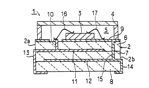
Fig. 1 is a cross section of a surface acoustic wave apparatus according to a
first preferred embodiment of the present invention.
Figs. 2A to 2C are plan views illustrating a structure of a phase unit disposed
in a l~min~ted ceramic substrate used in the first pl~felled embodiment.
Figs. 3A to 3C are impedance Smith charts at the input and output terminals
of the surface acoustic wave apparatus of the first preferred embodiment. Fig. 3A
is an impedance Smith chart at the terminal located at the side to which a phase unit
is connected. Fig. 3B is an impedance Smith chart at the terminal located at the side
opposite the side to which a phase unit is connected. Fig. 3C is an impedance Smith
chart in a case in which a phase unit is not connected.
Fig. 4 is a graph indicating the relationship between a relative dielectric
constant and a distance h between ground electrodes in a phase unit in a case in which
the phase unit having a characteristic impedance of 50Q is made from various ceramic
materials.
21~3012
Fig. 5 is a cross section of a surface acoustic wave apparatus according to a
second preferred embodiment of the present invention.
Figs. 6A to 6C are plan views illustrating a structure of a phase unit formed
in a l~min~ted ceramic substrate used in the second preferred embodiment of the
S present invention.
Fig. 7 is a cross section of a surface acoustic wave apparatus according to a
third preferred embodiment of the present invention.
Figs. 8A to 8E are plan views illustrating a structure of phase units formed
in a laminated ceramic substrate used in the third preferred embodiment of the present
invention.
Fig. 9 is a cross section of a surface acoustic wave apparatus according to a
fourth preferred embodiment of the present invention.
Figs. lOA to lOE are plan views illustrating a structure of phase units formed
in a l~min~ted ceramic substrate used in the fourth preferred embodiment of the
present invention.
First Preferred embodiment
Fig. 1 is a typical cross section of a surface acoustic apparatus according to
a first preferred embodiment of the present invention. In Fig. 1, there is shown a
surface acoustic wave apparatus 1. The shapes and the positions of a signal line,
ground electrodes, and through-hole electrodes disposed in a l~min~ted ceramic
substrate and to be described later are not necec~rily shown exactly or to scale.
2i 93al 2
In other words, to clarify the heights and the connections of these electrodes,
the surface shapes of these electrodes are roughly, not precisely, shown in Fig. 1.
The shapes and the positions of these electrodes are determined by plane shapes
shown in Figs. 2A, 2B, and 2C.
The surface acoustic wave apparatus 1 includes a l~min~ted ceramic substrate
2, a surface acoustic wave device 3 disposed on the l~min~ted ceramic substrate 2,
and a packaging member 4 for defining a package together with the l~min~ted ceramic
substrate 2. The packaging member 4 is secured on the l~min~ted ceramic substrate
2, and the l~min~ted ceramic substrate 2 and the packaging member 4 are arrangedto define a space 5 for accommodating the surface acoustic wave device 3.
The surface acoustic wave device 3 is not limited to any specific type, and can
comprise a transverse SAW filter, a SAW resonant filter, and a SAW resonator or
other surface acoustic wave device selected according to a particular desired usage.
The packaging member 4 is not limited to any specific type either, and can be
an a~plopliate packaging member made from m~teri~l.s such as a metal and a ceramic
m~teri~l including alumina and the m~teri~l used for the l~min~ted ceramic substrate
2 as long as it can define the accommodation space 5.
The present preferred embodiment features a ceramic used for the l~min~ted
ceramic substrate 2 and a phase unit built in the l~min~ted ceramic substrate 2. The
l~min~ted ceramic substrate 2 is preferably made from a low-permittivity dielectric
ceramic having a relative dielectric constant of about 7 or less. The above-described
dielectric ceramic can be used as a low-permittivity dielectric ceramic member.
219~01~
A preferred structure of the phase unit will be described below by referring
to Fig. 2. The l~min~d ceramic substrate 2 has a configuration in which ceramic
layers 6 to 8 are lamin~ted preferably in order from the top to the bottom.
On the ceramic layer 6, a first ground electrode 9 is formed as shown in Fig.
52A. The first ground electrode 9 is formed such that it extends between both end
edges 6c and 6d and the width of the electrode is preferably relatively wide, but it
does not extend to the side edges 6a and 6b. There exists an electrode-less area 9a
within the first ground electrode 9. A through-hole electrode 10 is located in the
electrode-less area 9a. The through-hole electrode 10 passes through the ceramic10layer 6 and is connected to a signal line 11 disposed below.
The signal line 11 is formed on the upper surface of the ceramic layer 7. As
clearly understood from Fig. 2B, the signal line 11 is formed to have an approximate
U shape such that it has a sufficient line length without extending the plane shape of
the ceramic layer 7, that is, without extending the plane shape of the lamin~tecl
15ceramic substrate 2. One end lla of the signal line 11 preferably extends to one end
surface 2a of the lamina~ed ceramic substrate 2.
On the upper surface of the ceramic layer 8, a second ground electrode 12 is
formed as shown in Fig. 2C. The second ground electrode 12 extends from one end
edge 8b of the ceramic layer 8 toward the other end edge 8a without reaching the end
20edge 8a. The second ground electrode 12 is formed such that it is relatively wider
than the signal line 11 and has the same width as that of the first ground electrode 9.
As shown in Fig. 1, in the l~min~ted ceramic substrate 2, an external electrode
13 is formed on one end surface 2a. The external electrode 13 is electrically
connected to the signal line 11. On the other end surface 2b, an external electrode
12
2i9301~
14 is formed. The external electrode 14 is electrically connected to the second
ground electrode 12. The first and second ground electrodes 9 and 12 are electrically
connected by a through-hole electrode 15. The through-hole electrode 15 is formed
such that it passes through the ceramic layers 6 and 7.
A phase unit is defined in the l~min~ted ceramic substrate 2 by the signal line
11 and the first and second ground electrodes 9 and 12.
The surface acoustic wave device 3 and the phase unit are electrically
connected by a bonding wire 16 and the through-hole electrode 10 shown in Fig. 1.
An electrode connected to the ground level of the surface acoustic wave device 3 is
electrically connected to the first ground electrode 9 by a bonding wire 17.
In the surface acoustic wave apparatus 1 of the present preferred embodiment,
since the phase unit is built within the l~min~ted ceramic substrate 2, an external
phase unit is not required for impedance matching of the surface acoustic wave device
3. Therefore, a circuit including the surface acoustic wave device 3 has a compact
construction.
Since the l~min~ted ceramic substrate 2 is made from the dielectric m~tPri~l
having a relative dielectric constant of about 7 of less, the distance between the
ground electrodes 9 and 12 can be made shorter while the width of the signal line 11
is the same, compared with a case in which a phase unit is formed in a conventional
l~min~tP~ ceramic substrate made from alumina. Therefore, the package has a low
profile while an increase in insertion loss is prevented. These advantages will be
more specifically described below with an example.
Figs. 3A and 3B show impedance Smith charts at the input and output
terminals of the surface acoustic wave apparatus 1 in which a phase unit having a
2 1 9 3 0 1 ~
-
characteristic impedance of 50Q is formed in the l~min~ted ceramic substrate 2. Fig.
3A shows the characteristics at a side to which a phase unit having a delay time of
0.3 ns is connected.
For comparison, Fig. 3C shows an impedance Smith chart at the input and
output terminals in a case when the phase unit is not connected to the surface acoustic
wave device.
As clearly understood from a comparison between the characteristics shown
Figs. 3A and 3C, the impedance at the transmission band (935 MHz to 960 MHz) is
smaller than that at a blocking band (890 MHz to 915 MHz), which has lower
frequencies that the tr~n~mi.~ion band, in the characteristics shown in Fig. 3A.It has been determined that by constructing a phase unit within the interior
of a l~min~ted ceramic substrate 2 made from ceramic materials having various
dielectric constants that the advantages of the preferred embodiments of the present
invention are obtained with the use of a m~teri~l having a relative dielectric constant
of about 7 or less. The distance h between the first and second ground electrodes was
measured in a case in which a phase unit having a characteristic impedance of 50Q
was built in a l~min~ted ceramic substrate made from various ceramic m~tçri~l~ with
a signal line having a width of 100, 130, 150, or 200 ,um being formed. Fig. 4
shows the results.
In Fig. 4, curve P indicates the result obtained when the width of a signal linewas set to 100 ~m, and curves Q, R, and S correspond to 130, 150, and 200 ~m,
respectively.
As clearly understood from Fig. 4, as compared with a case in which a highly
pure alumina substrate having a relative dielectric constant of 10 is used, the distance
~ ~ ~30 1 L
-
h between the first and second ground electrodes is reduced by one third or more in
a case when a phase unit of 50Q is made in the l~min~t~ ceramic substrate made
from a dielectric ceramic having a relative dielectric constant of about 7 or less. In
other words, even if a phase unit having the same thickness is made, the width of a
signal line can be extended by three ~m or more in a case when a dielectric material
having a relative dielectric constant of about 7 or less is used as compared with a case
when an alumina substrate is used. When the width of a signal line is extended, the
resistance thereof is reduced.
By using a low-permittivity ceramic to make a laminated ceramic substrate,
even when a phase unit is disposed within the interior of the device, a compact,phase-unit-built-in surface acoustic wave apparatus which is not susceptible to effects
caused by adjacent external circuits and components when mounted and in which anincrease in insertion loss is prevented can be provided.
In the foregoing example, the characteristic impedance of the phase unit was
set to 50Q. The same advantage can be obtained when a phase unit having a
characteristic impedance of another value is made.
Second Preferred Embodiment
Fig. 5 is a typical cross section of a surface acoustic apparatus according to
a second preferred embodiment of the present invention. Figs. 6A, 6B, and 6C areplans indicating an electrode system used for a phase unit formed in a l~min~tedceramic substrate. In Fig. 5, there is shown a surface acoustic wave apparatus 31.
The shapes and the positions of a signal line, ground electrodes, and through-hole
electrodes disposed in a multi-layer ceramic substrate 32 are shown roughly in order
2,~3~
to clarify the heights and the connections thereof, in the same way as in Fig. 1, which
shows the surface acoustic wave apparatus 1 of the first preferred embodiment. The
shapes and the positions of these electrodes are determined by plane shapes shown in
Figs. 6A, 6B, and 6C.
S The surface acoustic wave apparatus 31 of the second preferred embodiment
is preferably constructed in the same way as for the surface acoustic wave apparatus
1 of the first preferred embodiment except for the structure of a package formed by
a l~min~ted ceramic substrate and a packaging member. The same sections are
represented by the same reference numerals and the descriptions thereof will be
omitted.
In the surface acoustic wave apparatus 31, a l~min~ted ceramic substrate 32
and a packaging member 34 define a package structure and a space 5 which is defined
in the interior of the package accommodates a surface acoustic wave device 3.
The l~min~ted ceramic substrate 32 is preferably the same as the l~min~
ceramic substrate 2 of the first preferred embodiment in terms of having a structure
in which ceramic layers 6 to 8 are l~min~ted. On the ceramic layer 6, however,
substantially rectangular-frame-shaped ceramic layers 35 and 36 are preferably
disposed in the present preferred embodiment. In other words, the substantially
rectangular-frame-shaped ceramic layers 35 and 36 which have openings at the centers
are preferably disposed on the ceramic layer 6 in order to form the accommodation
space 5. The packaging member 34 is secured on the ceramic layer 36.
The ceramic layers 35 and 36 are preferably made from a dielectric ceramic
having a relative dielectric constant of about 7 or less in the same way as for the
16
23~301~
ceramic layers 6 to 8. They may be made from a ceramic having a relative dielectric
constant of more than about 7.
A through-hole electrode 15 is formed such that it passes through the ceramic
layers 35 and 36 and extends to the upper surface of the ceramic layer 36. In the
same way, a through-hole electrode 10 is formed such that it reaches the upper
surface of the ceramic layer 35 and is electrically connected to an electrode pad 37
formed on the upper surface of the ceramic layer 35.
Bonding wire 16 is connected to the electrode pad 37. An electrode pad 38
is also formed on the upper surface of the ceramic layer 35 in order to electrically
connect to the through-hole electrode 15. Bonding wire 17 is electrically connected
to the electrode pad 38.
In addition, a through-hole electrode 39 is formed such that it is electrically
connected to a first ground electrode 9 and it passes through the ceramic layers 35
and 36 to reach the upper surface of the ceramic layer 36.
Therefore, the through-hole electrode 39 and the through-hole electrode 15 are
connected to the ground level and are also connected to the packaging member 34 on
the upper surface of the ceramic layer 36. When the packaging member 34 is
preferably made up of, for example, a metal plate, an electromagnetic shield is
efficiently applied to the space 5. Not only a metal plate, but also a ceramic substrate
or a synthetic resin plate coated with electrically conductive film at least at the lower
surface may be used for the packaging member 34. When an electromagnetic shield
is not required, the packaging member 34 may be made up of an applop,iate,
insulating ceramic plate such as an alumina plate, or a synthetic resin plate.
2 1 ~30 1 ~
The surface acoustic wave apparatus 31 of the second preferred embodiment
is configured-in the same way as for the surface acoustic wave apparatus 1 of the first
preferred embodiment except for the points described above. In other words, the
multi-layer ceramic substrate 32 includes a signal line 11 and the first and second
ground electrodes 9 and 12. This means that a phase unit is built in the multi-layer
ceramic substrate 32. The ceramic layers 6 to 8 are preferably made from a
dielectric ceramic having a relative dielectric constant of about 7 or less. Therefore,
even when the phase unit is built in, an increase in insertion loss is avoided. A more
compact, phase-unit-built-in surface acoustic wave apparatus which is not susceptible
to effects of adjacent external circuits and components when mounted is
provided.
Third Preferred Embodiment
Fig. 7 is a typical cross section of a surface acoustic wave apparatus accordingto a third preferred embodiment of the present invention. Signal lines, ground
electrodes, and through-hole electrodes to be described later and disposed in a
l~min~ted ceramic substrate 52 have plane shapes shown in Figs 8A to 8E, but areroughly shown in Fig. 7 to make the corresponding positions in height clear. In other
words, the shapes and the positions of the signal lines, the ground electrodes, and the
through-hole electrodes are not precisely shown in Fig. 7. They actually have
cross-sectional structures corresponding to the structures shown in Figs. 8A to 8E.
A surface acoustic wave apparatus 51 is configured such that two surface
acoustic wave devices 53 and 54 are disposed on the l~min~ted ceramic substrate 52.
18
2193012
On the l~min~ted ceramic substrate 52, a packaging member 56 is also secured in
order to define an accommodation space 55.
In this preferred embodiment, the multi-layer ceramic substrate 52 preferably
includes two phase units having different distances between ground electrodes. By
referring to Figs. 8A to 8E, the preferred embodiment will be described in detail
below.
The multi-layer ceramic substrate 52 is preferably made from a dielectric
material having a relative dielectric constant of about 7 or less and has a structure in
which ceramic layers 57 to 61 are l~min~ed in order from the top to the bottom.
On the upper surface of the ceramic layer 57, a first ground electrode 62 is
formed as shown in Fig. 8A. Electrode-less areas 62a and 62b are provided withinthe first ground electrode 62. Through-hole electrodes 63 and 64 passing through the
ceramic layer 57 are formed in the electrode-less areas 62a and 62b, respectively.
Through-hole electrode 64 further passes through the ceramic layers 58 and 59 toextend downwardly and is electrically connected to a signal line 69 to be described
later. The first ground electrode 62 is formed such that it does not extend to both
side edges of the ceramic layer 57 but has a width and a shape such that it almost
extends to the side edges, and it extends to both end edges 52a and 52b of the
multi-layer ceramic substrate 52.
As shown in Fig. 8B, a signal line 65 is formed on the ceramic layer 58 with
a thinner line than that of the ground electrode 62. As clearly understood from Fig.
8B, the signal line 65 has a curved shape in which a part of a substantially
rectangular frame is missing, thereby the signal line 65 has a sufficient length without
extending the plane shape of the ceramic layer 58.
19
2 1 ~3Q 1 ~
In the vicinity of an inner end 65a of the signal line 65, the through-hole
electrode 63 is electrically connected to the signal line 65. The other end of the
signal line 65 extends to an end surface 52a of the l~min~ted ceramic substrate 52 and
electrically connected to an external electrode 66. The external electrode 66 isSformed on an end surface 52a of the l~min~ted ceramic substrate 52 and extends to
the lower surface of the l~min~ted ceramic substrate 52.
A common ground electrode 67 is formed on the upper surface of the ceramic
layer 59 as shown in Fig. 8C. The common ground electrode 67 is formed such thatit has the same width as the first ground electrode 62 and it does not extend to an end
10surface 52a of the l~min~ted ceramic substrate 52. The common ground electrode 67
extends to an end surface 52b only and is electrically connected to an external
electrode 68 shown in Fig. 7. The common ground electrode 67 may extend to an
end surface 52a unless it touches the signal line. The external electrode 68 is formed
such that it extends from an end surface to the lower surface of the l~min~ted ceramic
15substrate 52 in the same way as the external electrode 66.
The first ground electrode 62 is connected to the common ground electrode
67 by the through-hole electrode 76 passing through the ceramic layers 57 and 58.
The common ground electrode 67 has an electrode-less area 67a. At the
electrode-less area 67a, the through-hole electrode 64 described above passes through
20in a downward direction.
As shown in Fig. 8D, a signal line 69 is formed on the upper surface of the
ceramic layer 60. The signal line 69 is formed by a narrow line-shaped electrodesuch that it has a smaller area than the common ground electrode 67. Since the signal
2i93Q12
line 69 has an approximate U shape, it has a sufficient length without extending the
plane shape of the ceramic layer 64.
The through-hole electrode 64 is electrically connected to an inner end of the
signal line 69. The other end of the signal line 69 extends to an end surface 52a of
the l~min~ted ceramic substrate 52 and electrically connected to an external electrode
70. The external electrode 70 is formed in a different area from that for the external
electrode 66 on an end surface 52a.
A second ground electrode 71 is formed on the upper surface of the ceramic
layer 61. The second ground electrode 71 extends from an end surface 52b toward
an end surface 52a of the l~min~ed ceramic substrate 52 but does not reach an end
face 52a. The second ground electrode 71 has the same width as the common groundelectrode 67. The second ground electrode 71 may extend to an end surface 52a.
In the multi-layer ceramic substrate 52, two phase units are preferably formed
in the vertical direction with the common ground electrode 67 used in by both phase
units. One phase unit includes the signal line 65, the first ground electrode 62, and
the common ground electrode 67, and the other phase unit includes the signal line 69,
the common ground electrode 67, and the second ground electrode 71. Since the
common ground electrode 67 is used in common as one of the ground electrodes of
each of the upper and lower phase units, the multi-layer ceramic substrate 52 is made
relatively thin despite the fact that two phase units are arranged in the vertical
direction.
In addition, the ceramic layers 59 and 60 are preferably made thinner than the
ceramic layers 57 and 58. Therefore, the distance hl between the ground electrodes
(between the ground electrode 62 and the common ground electrode 67) in the upper
2193:)12
phase unit is larger than the distance h2 between the ground electrodes (between the
common ground electrode 67 ad the second ground electrode 71) in the lower phaseunit.
Since the distances h, and h2 between the ground electrodes in the phase units
S disposed in the vertical direction differ, the two phase units have different
characteristic impedances.
According to the present preferred embodiment, a plurality of phase units
having different characteristic impedances are easily configured in the multi-layer
ceramic substrate 52 by differentiating the ground-electrode distance of one phase unit
from those of the other phase units. Therefore, according to the characteristics of a
surface acoustic wave device used, a phase unit having the most suitable characteristic
impedance can be readily constructed.
The surface acoustic wave device 53 secured on the multi-layer ceramic
substrate 52 is electrically connected to the through-hole electrode 63, that is, to the
phase unit disposed at the upper side, by a bonding wire 72. The surface acoustic
wave device 54 is electrically connected to the through-hole electrode 64, that is, to
the phase unit disposed at the lower side, by bonding wire 75. The surface acoustic
wave devices 53 and 54 are electrically connected to the ground level by bondingwire 73 and 74, respectively.
Also in this preferred embodiment, since the phase units are disposed within
the l~min~ted ceramic substrate 52 as described above and the l~min~ted ceramic
substrate 52 is made from a dielectric ceramic having a relative dielectric constant of
about 7 or less, a more compact, phase-unit-built-in surface acoustic wave apparatus
which elimin~tes an increase in insertion loss and is not susceptible to effects of a
~i93012
adjacent electronic circuits and components when mounted is provided as in the first
and second preferred embodiments.
Fourth Preferred Embodiment
S Fig. 9 is a typical cross section of a surface acoustic wave apparatus according
to a fourth preferred embodiment of the present invention. Figs. lOA to lOE are
plans illustrating electrode shapes on the upper surfaces of ceramic layers which
constitute phase units in a l~min~tecl ceramic substrate used for the surface acoustic
wave apparatus shown in Fig. 9.
Cross-sectional structures shown in Fig. 9 are roughly illustrated in order to
facilitate the understanding of the positions and connections of signal lines, ground
electrodes, and through-hole electrodes to be described later, as in Fig. 7. They are
not necess~rily shown precisely in Fig. 9. The plane shapes of the signal lines, the
ground electrodes, and the through-hole electrodes are shown in Figs. lOA to lOE.
A surface acoustic wave apparatus 81 is configured in the same way as for the
surface acoustic wave apparatus 51 of the third preferred embodiment except that a
package structure formed by a l~min~ted ceramic substrate and a packaging memberis different. The same portions as those in the surface acoustic wave apparatus 51
of the third preferred embodiment are indicated by the same reference numerals, and
the detailed descriptions thereof will be omitted.
In the surface acoustic wave apparatus 81, the package structure is formed by
the l~min~te~ ceramic substrate 82 and the plane packaging member 83. In the
accommodation space 55, two surface acoustic wave devices 53 and 54 are formed.
21 9301 2
- The l~min~ted ceramic substrate 82 has a structure in which ceramic layers 57
to 61 are l~min~ted. On the upper surfaces of the ceramic layers 57 to 61, ground
electrodes, signal lines, and through-hole electrodes are formed as shown in Figs.
10A to 10E in the same way as for the surface acoustic wave apparatus 51 of the
third prefell~d embodiment. The present preferred embodiment differs from the third
preferred embodiment in that ceramic layers 84 and 85 are further formed above the
ceramic layer 57.
The ceramic layer 84 has a substantially-rectangular-frame shape including two
substantially rectangular openings at the center in plane. A surface acoustic wave
device 53 is disposed in one opening and a surface acoustic wave device 54 is
disposed in the other opening. The ceramic layer 85 has a substantially
rectangular-frame shape including a large opening at the center in plane. The ceramic
layers 84 and 85 may be made from the same ceramic material as the ceramic layers
57 to 61, or other ceramic material having a relative dielectric constant of about 7 or
more.
Through-hole electrodes 63 and 64 extend to the upper surface of the ceramic
layer 84 and are electrically connected to the surface acoustic wave devices 53 and
54 on the upper surface of the ceramic layer 84 by bonding wires 72 and 75,
respectively. At a partitioning wall 84a disposed at the center of the ceramic layer
84, a through-hole electrode 86 passing through the ceramic layer 84 is formed. The
through-hole electrode 86 is electrically connected to a first ground electrode 62, and
also electrically connected to bonding wire 73 and 74.
Through-hole electrodes 87 and 88 are formed such that they penetrate the
ceramic layers 84 and 85. The through-hole electrodes 87 and 88 are electrically
24
~1 9301 2
`~ connected to the substantially rectangular-frame-shaped shield electrodes 89 and 90
on the upper surfaces of the ceramic layers 84 and 85, and are also electricallyconnected to the first ground electrode 62 at their lower ends.
The packaging member 83 is preferably made up of a metal plate or an
insulating plate of which the lower surface is covered with electrically conductive
film, and is formed such that it electromagnetically shields an accommodation space
55. The packaging member 83 may be made up of a synthetic resin plate or an
insulating ceramic plate.
Since the surface acoustic wave apparatus 81 of the fourth preferred
embodiment is configured in the same way as for the surface acoustic wave apparatus
51 of the third preferred embodiment except that the above-described package
structure is used, even when phase units are constructed within the package structure,
an increase in insertion loss is prevented. The surface acoustic wave apparatus 81
serves as a more compact surface acoustic wave apparatus which has built-in phase
units and is not susceptible to effects of a adjacent external circuits and electronic
components when mounted. In addition, in the same way as for the third preferredembodiment, since the characteristic impedances of phase units disposed at the upper
and lower positions can easily be changed, phase units best suited to the surface
acoustic wave devices used can be readily configured.
While the invention has been particularly shown and described with reference
to preferred embodiments thereof, it will be understood by those skilled in the art that
the foregoing and other changes in form and details may be made therein without
departing from the spirit and scope of the invention.