Note: Descriptions are shown in the official language in which they were submitted.
WO g~'C~ I~G 2 1 9 3 0 6 9 PCT/US95/09079
THYRISTOR POWER CONTROL CIRCUIT
BACKGROUND OF THE INVENTION
The present invention relates generally to thyristors used in electronic switching
circuits and power controllers and relates more particularly to silicon controlled rectifiers
5 and triacs used as a controlled switch in commercial and household electronic devices for
applying power from AC power lines.
Thyristors are i"teg"lted-circuit components that are used to control the application
of electrical power to a load. In effect, they function as electronic switches. Triacs and
silicon controlled rectifiers (SCRs) are varieties of thyristors. The triac functions as a
10 bidirectional alternating-current switch, and the SCR functions as a uni-directional switch
permitting rectified current flow in one direction only. Triacs and SCRs are found in many
industrial and consumer products in such uses as light dimmers, motor speed controllers,
heater controllers, or simply controlled switches for applying electrical power in response
to the happening of some event.
The problems addressed by the present invention will be more readily understood
if ~iscussed in a specific example. They are illustrated here in the example of a passive
infrared (PIR) motion detector, although the same problems and concerns arise in a
variety of applications. A PIR motion detector is a device used in automatic light switches
and security systems to turn on a light or to activate some other form of alarm or warning
20 indicator when a person or motor vehicle enters a monitored area. Such devices are used
with outdoor residential lighting, for example, to illuminate a walkway as a person
approaches the front door or to illuminate a driveway as a car approaches.
The PIR motion detector functions by sensing heat in the form of infrared radiation
emanating from a person or similarly warm object as the person or object enters or moves
25 about in the field of view of the detector. When the motion detector detects an appropriate
heat impulse characteristic of a moving heat source, it provides an electrical signal to
activate the light or other alarm. This electrical signal is generally a low-voltage signal,
typically on the order of 5 to 15 Volts, that does not carry sufficient power to energize the
typical electric lights used for interior or exterior building lighting. Household lighting is
30 generally designed to be energized at 120 Volts. This is the nominal voltage of the
electrical service provided by local utility companies throughout the United States. To
overcome this deficiency, the low-voltage signal developed by the motion detector
(sometimes referred to as a triggering or gating signal) is applied to a switching
component, which responds by permitting electric current to flow through the lights at the
W095~0~19v - ~ ' 2 1 93069 PCT/U595/'~3~75~
higher 120-Volt level of the power line. The triac is a common switching component used
for this purpose, and the SCRis often used where uni-directional current is desired.
While the triac and the SCR have proven to be reliable and popular switching
components in motion detectors and other electronic products, they nevertheless have
5 their limitations. Usually a special firing circuit is needed to "fire" or gate the triac (SCR)so
that it conducts at the higher voltage of the power mains. The firing circuit desirably
provides a "clean" gating signal that is comparatively insensitive to line fluctuations, noise
transients or other irregularities to provide unambiguous triggering of the triac (SCR). In
addition, the triac and SCR do not necessarily pass all the power of the line current
10 through to the load. The average power that the triac (SCR) applies to the load depends
on when the triac (SCR)is fired during the alternating current cycle. Triac and SCR firing
circuits commonly include a phase-control circuit and may also include a zero-crossing
detector for establishing a desired phase relationship between the triac (SCR) gate signal
and the applied AC line voltage. This phase relationship determines the proportion of the
15 AC waveform (and hence the average power) that is applied to the load per AC cycle.
The need for a triac (SCR) firing circuit ultimately increases cost of the product.
More coll,plicated firing circuits generally require a greater number of circuit components
and make greater demands on product assembly or are provided by more costly
specialized integrated-circuit chips. For low-cost household and consumer products the
20 extra cost of the triac (SCR) firing circuit is significant and increases the price at which the
product may be offered to the end user. Nevertheless, in the past the need for special
(and often complex) thyristor firing circuits for efficient and reliable thyristor operation
could not be avoided.
Another constraint on the use of thyristors is the need for precautions against
25 electrical shock. For a household or commercial product to receive approval from
regulatory safety-testing organizations, the 120-Volt line voltage must be properly isolated
within the product to prevent injury in the event of a malfunction. Thus, for example, to
achieve efficient triac firing while sufficiently isolating the triac firing circuit and the rest of
the product's low-voltage circuitry from the 120-Volt line voltage, specialized integrated-
30 circuit triac firing chips have been developed, such as the MOC 3010 optical driver. Thischip fires the triac reliably at the desired time (i.e., phase relationship) and provides an
optical link between the low and high-voltage circuits that protects quite well against
dangerous, undesired electrical connections between the two circuits. The MOC 3010
optical driver chip successfully meets the dual technical demands of reliable, precise triac
~, /q3J o~CI
firing and safety. For use in a low-cost household or
commercial product, however, it has the disadvantage of
high cost.
SUMMARY OF THE INVENTION
The present invention provides a circuit arrangement
and method for firing a gated thyristor such as a triac
or SCR that meets the demands of reliable firing and
circuit isolation with a comparatively few low-cost
circuit components and avoids the need for specialized
firing chips such as the MOC 3010, zero-crossing
detectors, or other more complicated circuit arrangements
previously used.
Accordingly, the present invention provides control
circuitry for applying electrical power from a live power
lead and a neutral power lead to a load in response to a
trigger signal, comprising: a thyristor having first and
second main terminals and a gate terminal, said thyristor
having a characteristic threshold potential for enabling
current flow between said first and second main
terminals, a first of said first and second main
terminals being connected to said live power lead, the
other of said first and second main terminals being
connected to a first side of said load, and said neutral
power lead being connected to a second side of said load;
biasing means for biasing said live power lead at a
negative potential with respect to said neutral power
lead and defining a circuit ground substantially at said
negative potential; and gate circuit means connected
between said gate terminal and said circuit ground for
applying a gate potential at least as great as said
characteristic threshold potential to said gate terminal
in response to said trigger signal.
In a further aspect the present invention provides a
method for applying electrical power from a live power
lead and a neutral power lead to a load in response to a
trigger signal, comprising the steps of: providing a
k
~, /q3~ o/O~
thyristor having first and second main terminals and a
gate terminal, said thyristor having a characteristic
threshold potential for enabling current flow between
said first and second main terminals; applying one of
said first and second main terminals to said live power
lead, applying the other of said first and second main
terminals to a first side of said load, and applying said
neutral power lead to a second side of said load;
biasing said live power lead at a negative potential with
respect to said neutral power lead to define a circuit
ground at said negative potential; and applying a gate
potential at least as great as said characteristic
threshold potential to said gate terminal in response to
said trigger signal, said gate potential being negative
with respect to said neutral power lead.
The circuit arrangement of the invention is used for
applying electrical power to a load in response to a
trigger signal, from a live power lead and a neutral
power lead such as found in the common household
electrical service. Briefly, the circuit arrangement
includes a gated thyristor having first and second main
terminals and a gate terminal. The load to be energized
in response to the trigger signal is connected between
the neutral power lead and one of the thyristor main
terminals, the other thyristor main terminal being
connected to the live power lead. The live power lead is
biased at a negative potential with respect to the
neutral power lead to define a circuit ground
substantially at the negative potential. A gate circuit
is connected between the gate terminal and the circuit
ground for applying a potential to the gate terminal in
response to the trigger signal that is at least as great
as the thyristor's characteristic threshold potential for
enabling current flow between the thyristor main
terminals and thereby energizing the load. The potential
applied to the gate terminal is thus negative with
recpect to the neutral power lead. In one embodiment the
3a
~, 193, ~f~9
gate circuit may be as simple as a single transistor
switched on by the trigger signal and connected in line
with a diode and resistor between the gate terminal and
the circuit ground. This arrangement provides a
particularly low cost method for firing the thyristor
while providing electrical isolation of the low voltage
parts of the apparatus from the power line voltage.
Other aspects, advantages, and novel features of the
invention are described below or will be readily apparent
to those skilled in the art from the following
specifications and drawings of illustrative embodiments.
BRIEF DESCRIPTION OF THE DRAWINGS
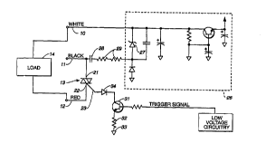
FIG. 1 is an electrical circuit schematic diagram
showing a triac arrangement according to the invention.
3b
'~
WO 96/00490 PCT/US95/09079
2 1 93069
DETAILED DESCRIPTION OF ILLUSTRATIVE EMBODIMENTS
The typical household 120-volt electrical service is provided over two lines, one of
which (referred to as the neutral line) is maintained at Earth potential by the local utility
company and the other of which is "live" or "hot" with respect to the neutral line. In the
5 circuit arrangement of FIG. 1 lead 10 is a neutral power lead intended to be connected to
the neutral, grounded line from the utility company, and lead 11 is a live power lead
intended to be connected to the live line from the utility company. Lead 12 is a switched
lead, which is connected to live lead 11 according to the invention through gated
thyristor 13. In FIG. 1 the leads 10, 11 and 12 are labeled "white," "black" and "red,"
10 respectively, which are common colors for these leads in household and commercial
products. A load 14 is connected between the neutral and switched leads 10 and 12. In
the example of the PIR motion detector described above, the load is provided by the light
to be energized when motion is detected. In other applications the load may be provided
by a motor, heating element, or such other unit requiring the high-voltage power supply
15 from the utility company. Line 16 carries a low-voltage trigger signal developed by the
low-voltage circuitry 17. The triggering signal indicates when load 14 is to be energized. In
the above motion detector example, low-voltage circuitry 1i is provided by the circuitry for
sensing the motion, conditioning and filtering intermediate electrical signals, and
generating the trigger signal indicating that motion has been detected. In other20 applications the low-voltage circuitry 17 will be appropriate to the functions of the
particular application. In typical household and commercial products the low-voltage
circuitry operates at a nominal voltage of 5 to 15 volts. In the present context"low-voltage" refers to voltage sufficiently lower than the line voltage applied across
load 14 that a goveming safety-testing authority would require the low-voltage circuitry to
25 be isolated from the line voltage.
In FIG. 1 thyristor 13 is provided by a triac having first and second main
terminals 21 and 22 and a gate terminal 23. The terms "first and second main terminals"
are used herein to distinguish the main conduction terminals from the gate terminal. They
are used herein to refer also to the anode and cathode terminals of an SCR or other uni-
30 directional thyristor and are generally used in this context without reference to which is thecathode and which is the anode. Those skilled in the art will readily be able to identify the
cathode and anode according to the desired SCR polarity. In the embodiment of FIG. 1
thyristor main terminal 21 iS connected to live lead 11 and main terminal 22 is connected
to the switched live lead 12.
wo ~ c~ ,9~ ' 2 1 9 3 0 6 9 PCT/U~5~0~79
The arrangement of FIG. 1 includes a low-voltage power supply indicated generally
at block 26 for supplying power to low-voltage circuitry 17. Unlike the common practice in
the past, the low-voltage power supply 26 in FIG. 1 biases the live lead 11 at alow-voltage reference value below the neutral lead 10. This is accornplished in FIG. 1 by
Zener diode 27, which is connected between neutral lead 10 and live lead 11 withappropriate polarity to bias live lead 11 at a negative potential with respect to the neutral
lead. Specifically, the cathode side of Zener diode 27 is connected to neutral line 10 and
the anode side is connected to live lead 11 through current limiting capacitor 28 and
resistors 29, which are provided for safety in the event of a short circuit. Although the
Zener diode biasing arrangement shown in FIG. 1 is desirable because of its low cost,
those skilled in the art will recognize that other voltage regl~lation methods may also be
used for maintaining the live lead at the desired negative reference potential below the
neutral lead.
In FIG. 1 the thyristor gate current from gate terminal 23 is controlled by a gate
circuit comprising transistor 31 and resistor 32. Transistor 31 is switched between its
conducting and blocked states by the low-voltage trigger signal along line 16, which is
applied to the base of transistor 31.
In operation, when there is no signal on line 16, transistor 31 is off. No gate
current is then present at gate terminal 23, triac 13 is non-conducting, and the switched
line 12 is de-energized. When the trigger signal on line 16 goes high, transistor 31
conducts, allowing gate current at gate terminal 23 to short through resistor 32 to the
circuit ground at 33. Unlike the co"""on practice in the past, the circuit ground at 33 is
actually at the potential of the live line 11, less an insignificant diode junction voltage. In
the embodiment of FIG. 1 transistor 31 acts as a current sink. Those familiar with
conventional thyristor operation and terminology will recognize that in the circuit
arrangement of FIG. 1 the triac is fired in quadrants ll and lll, and this is accomplished
without the need for special phase-shift circuitry.
Normally when gate terminal 23 is conducting, the current generated would be
sufficient to destroy the gate circuit--in this case transistor 31, in particular. In the past it
has been common to use zero-crossing detectors or phase-control circuitry to shut off the
triac firing circuit before it can suffer damage. In the embodiment of FIG. 1 transistor 31 is
protected from damage by diode 34 in line with transistor 31. When diode 34 is
conducting, transistor 31 is effectively shorted out. The value of resistor 32 is selected to
pull sufficient current to fire triac 13, typically on the order of 7.5 milliamperes, without
damaging transistor 31. As resistor 32 pulls more current, the potential across the resistor
wo g~ o ~ i i . ; 2 1 9 3 0 6 9 PCT/US95/09079
rises to the point where transistor 31 regulates the current level to maintain thyristor
conduction.
The specific component values for the various resistors, capacitors and other
components shown in FIG. 1 depend on the particular choice of thyristor and trigger signal
5 characteristics as well as the intended operating environment. Determination of
appropriate component values for a particular application is well within the ordinary skill in
the art and need not be described here.
The arrangement of FIG. 1 has a number of advantages that should now be
evident. The need for triac predrivers or similar such controllers is eliminated. The circuit
10 is simplified to the point that the triac firing mechanism is effectively provided by a single
transistor and diode. For mass-produced products this can represent a significant savings
in cost. Notwithstanding the simplified circuitry, the high-voltage lines are protected from
applying a high potential difference across the low-voltage circuitry.
The above descriptions and drawings disclose illustrative embodiments of the
15 invention. Given the benefit of this ~isclosure, those skilled in the art will appreciate that
various modifications, alternate constructions, and equivalents may also be employed to
achieve the advantages of the invention. For example, although the single transistor 31
and resistor 32 arrangement of FIG. 1 is particularly simple and cost effective, those
skilled in the art will be able to devise other bipolar and field-effect transistor
20 configurations for driving the thyristor gate current according to the invention. In certain
applications, particularly for SCR configurations, it may also be desirable to connect the
main terminals to the power leads through diodes. In addition, the gating circuitry can be
configured to respond to various trigger signal levels and characteristics for more complex
levels of control than illustrated herein. Therefore, the invention is not to be limited to the
25 above description and illustrations, but is defined by the appended claims.