Note: Descriptions are shown in the official language in which they were submitted.
WO 96/00979 ~ ~ 1~ ~ ~ PCT/GB95/01541
1
PREPARATION OF SEMICONDUCTOR SUBSTRATES
The present invention relates to the production of semiconductor devices
and in particular to the preparation of indium phosphide semiconductor
substrates
for use in the production of semiconductor devices using MOVPE techniques.
MOVPE (Metal Organic Vapour Phase Epitaxy) is commonly used to grow
a wide variety of semiconductor devices comprising multiple layers which
require
precise material composition and thickness. In some materials systems,
virtually
monolayer control can be achieved using MOVPE when switching from one
compound to another which in some cases is essential for accurate, repeatable
device fabrication. The achievable purity of deposited layers using MOVPE is
potentially very high but can be affected by the purity of the starting
products. As
long as the starting products are not totally pure, device manufacturers have
to
take steps to avoid or counter the unpredictable effects that the impurities
have on
manufacturing processes, or suffer from reduced device yield.
It has been shown that epitaxially deposited III-V semiconductors
commonly suffer from the presence of conductive interfacial layers at the
substrate interface f 11.
This phenomenon presents a particular problem to InP based field effect
transistors (FETs) grown on Fe-doped InP substrates because it prevents pinch-
off
by providing a parallel conduction path that cannot be controlled by gate
voltage.
This also raises output conductance, device-to-device leakage and can add a
parasitic capacitance affecting high frequency performance.
Conducting interfacial layers can have many origins, however, the
strongest recent evidence indicates accumulation of Si atoms at the
substrate/epitaxial layer interface to be the major culprit f 1 ]. Interfacial
impurities
have been variously attributed to out diffusion from the substrate, residues
from
substrate preparation solutions and contamination from ambient air. In
addition,
the inventors have observed Si accumulation in an MOVPE kit for several weeks
following refurbishment of the vent-run gas switching manifold. Even when
below
detection limits in grown layers, this is another potential source of surface
contamination during wafer heat-up. In practice, it is quite likely that
several of
these mechanisms may contribute to contamination simultaneously, varying in
WO 96/00979 ~ ~ PCTlGB95/01541
2
degree of severity depending on factors such as the substrate batch or
manufacturer, its handling and preparation procedure, chemical batches and the
history of the growth kit.
The significance of the accumulated silicon greatly increases as device
complexity increases, since fabrication times increase giving the silicon more
time
to accumulate. Therefore, the production of highly integrated monolithic
semiconductors including, for example, HFET (heterojunction field effect
transistors), lasers and transmitters, HEMTs (high electron mobility
transistors) and
OEICs (opto-electronic integrated circuits) has highlighted the need to
overcome
the problem.
Many workers have developed processes for mitigating parallel conduction
in FETs and HEMTs. Recently, H. Ishikawa et al in "Origin of n-type conduction
at
the interface between epitaxial-grown layer and InP substrate and its
suppression
by heating in phosphine atmosphere", J. Appl. Phys 71 (8), 15 April 1992, pp
3898-3903, described a study into the origins of n-type conduction due to Si
atoms at the epitaxial layer-substrate interface. In the study Ishikawa et al
theorised that Si atoms originated in the air, possibly from the filters used
in clean
rooms, and became adsorbed into the InP. The adsorbed Si subsequently
accumulated at the epitaxial layer-substrate interface and manifested itself
as
n-type impurities causing n-type conduction at the boundary. To counter this,
Ishikawa et al proposed a method of removing the atoms from the InP substrate
by
annealing it in a PH3 atmosphere, The process involved heating the InP to a
temperature of around 700°C for 20 minutes with a PH3 flow rate of
1200sccm.
The results indicated that a high proportion of the Si atoms adsorbed into the
InP
surface were desorbed, which reduced the effect of n-type Si conduction.
In another paper, "Highly Resistive Iron-doped AIInAs layers grown by
Metalorganic Chemical Vapour Deposition", J. Appl. Phys. Vol. 31 (1992) pp
L376-L378, Ishikawa et al described a method of fabricating a semi-insulating
iron-doped AIInAs buffer layer on an InP substrate prior to the deposition of
further
epitaxially-grown layers. By this method, the influence of the substrate
itself, over
the epitaxially-grown layers, is mitigated.
Although the existence of parallel conduction mechanisms has been
recognised for at least 10 years, and more recently the causes of the
mechanisms,
WO 96/00979 ~ ~ 9 3 ~ 9 8 PCT/GB95I01541
3
for example n-type conduction by silicon atoms, have been isolated,
surprisingly,
none of the proposed methods of overcoming or countering the effects of the
mechanisms have proved entirely satisfactory. In such a rapidly growing and
important field as III-V semiconductor device fabrication, a method of
successfully
and reproducibly fabricating devices without parallel conduction mechanisms
would
be of extreme commercial importance.
Therefore, in accordance with one aspect, the present invention provides a
method of preparing a semiconductor substrate for subsequent growth of
epitaxial
layers, the method comprising the steps of, annealing the substrate to reduce
the
concentration of impurity atoms present on or in the substrate, and
thereafter,
growing one or more buffer layers on the substrate, the or at least one of the
buffer layers comprising a semiconductor material doped with metal atoms.
The annealing step promotes any tendency for surface accumulation of
impurities, for example silicon atoms, by diffusion from the bulk substrate.
Also,
annealing promotes impurity atom removal from the substrate surface.
For the example of annealing an InP substrate, impurity atoms, for
example silicon atoms, in or on the substrate are replaced with phosphorus
atoms.
The annealing is carried out at a temperature which is high enough to promote
high
mobility of surface atoms on the substrate. The phosphorus atoms are
transported
in a flow of gaseous phosphine, or other suitable phosphorus containing
compound
which yields phosphorus atoms, the flow rate being great enough to maintain an
overpressure which prevents net loss of phosphorus atoms due to heating. It
has
been shown [2] that the rate of removal of silicon impurity atoms is
proportional to
the heating time, the heating temperature and the flow rate of phosphine.
Therefore, the maximum benefit from annealing can be achieved by maximising
the
values in the annealing process. However, the values should in practice be set
for
practicality, i.e. so that the annealing step does not take too long,
phosphine flow
is not so high that filters become blocked, etc. It is expected that some
benefit
' would accrue at a temperature as low as 600°C, for a time as short as
5 minutes
and with the minimum phosphine flow sufficient to stabilise the InP surface at
the
anneal temperature.
WO 96/00979 219 3 0 9 8 PCT/GB95101541
4
Substrates other than InP are typically annealed in atmospheres comprising
other suitable conditions. For example, for a GaAs substrate, the annealing
step is
carried out in an atmosphere typically comprising arsine.
It is clear that strict compliance with specific values for the annealing
process is not necessary and that the values may be traded off against each
other.
For example, a higher heating temperature would require a shorter heating
time.
The buffer layer (or layers) provides) a semi-insulating barrier between the
substrate and subsequently grown epitaxial layers to reduce the influence the
substrate has over the nature and performance of the subsequently grown
epitaxial
layers.
For III/V compounds such as doped GaAs or doped GaAIAs,
semi-insulating layers can be epitaxially grown by MOVPE by varying the III/V
ratio.
Increasing the III/V ratio alters doped p-type GaAs or GaAIAs to n-type GaAs
or
GaAIAs, and vice versa. Near the point of conversion, the GaAs or GaAIAs
exhibits high resistivity and can thus act as a semi-insulating layer.
In the case of undoped InP, layers grown by MOVPE generally show
n-type conduction indicating that undoped AIInAs layers cannot form highly
resistive (semi-insulating) buffer layers by varying the III/V ratio. However,
it has
been shown that doping an InP layer with iron reduces n-type conduction in the
InP. This is also the case with doping AIInAs with iron.
It has been shown that iron atoms cancel the affects of n-type carriers, in
effect forming 'carrier traps', and that the higher the iron concentration,
the
greater the insulating properties of the iron doped InP or AIInAs f3].
At least one buffer layer is deposited on the semiconductor substrate
using MOVPE growth techniques. In the case of InP, the buffer layer is doped
with
iron to increase the resistance of the buffer layer by allowing the
electrically active
iron atoms to act as deep carrier traps for the n-type carriers.
Alternatively, other
semi-insulating dopants such as cobalt (Co) and rhodium (Rh) are expected to
be
effective alternatives dopants to iron to act as n-type carrier traps,
although, in
most cases the resistivity of the InP will be lower.
Other dopants, for example chromium, have been seen to act as p-type
carrier traps in InP and GaAs. In general, for a dopant to act as an effective
carrier
trap, it is a requirement that it sits as closely as possible to the centre of
the band-
. , ..
2193098 - .. _. ,-
gap of the base material in which it is doped. Then, the dopant, and hence any
trapped carriers, are as far away as possible from both the valance and
conduction
bands of the base material making carrier escape through thermal or electrical
. excitation difficult. As a result, the doped base material increases greatly
in
5 resistivity. Obviously, a dopant is selected for its ability to act either
as a p-type
carrier trap or as an n-type carrier trap in dependence on the type of
conduction,
for example due to the presence of impurities, exhibited by the base material.
The inventors have shown that a combination of annealing and a
subsequently grown semi-insulating buffer layer is an effective method of
greatly
reducing the effects of conducting interfacial layers, in most cases. However,
in
some cases, for example in a case where a substrate boule proves to be
particularly susceptible to parallel conduction mechanisms, a further step is
included in the preparatory stages of a substrate to offer greater protection
against
the vagaries of substrate quality.
The further step is an etch step, which is carried out between the
annealing step and the buffer layering step. The etch step removes any surface
contaminants from the substrate, for example oxygen or oxides which may have
contaminated the substrate from the atmosphere in which the boule is stored or
transported, and provides a clean, flat surface on which subsequent epitaxial
layers can be grown. The inventors have shown that any etching process, and
indeed any etchant, for example phosphorus trichloride to etch InP, which is
shown to provide non-preferential etching (i.e. polish etching), without
unduly
roughening the substrate surface, is suitable for the etching step. The
inventors
have also shown that gas-etching provides better results than wet-etching
because
gas-etching is carried out in-situ, providing exclusion of impurities that may
re-contaminate the surface of the substrate. Preferably, no more than about
l,um
(that is to say, the first few monolayers) of surface substrate is removed to
provide a substrate surface of the required cleanliness.
The invention will now be described in greater detail, by way of example,
with reference to the following drawings, in which:
Figure 1 shows a typical HFET structure;
Figure 2 shows typical capacitance/voltage depth profiles of HFETs tested
in the course of experiment; and
A~~~F~~Ed S~E~.S
WO 96100979 219 3 0 9 8 pCT/GB95/01541
6
Figure 3 shows a typical set of HFET characteristics obtained from an
HFET fabricated on a substrate prepared according to the present invention.
An iron-doped InP substrate was prepared for subsequent epitaxial HFET
device growth as follows.
The iron-doped InP substrate was installed in an atmospheric pressure
MOVPE reactor. For the annealing stage, the substrate was heated to a
temperature of around 750°C, in the reactor, in an atmosphere of
phosphine and
highly pure hydrogen.
At around 400°C the surface of an InP substrate becomes unstable
unless
phosphine or a similar gas is present in the atmosphere to stabilise the
surface.
Typically, therefore, a phosphine flow should be present during the whole
substrate heating process, or at least from around 400°C upwards.
The rate of impurity silicon atom removal from a substrate due to the
annealing step has been reported to be proportional to the heating time and
substrate temperature [21.
The substrate was annealed at 750°C for 30 minutes with a
phosphine
flow of 46sccm (standard cubic centimetres per minute), to provide a partial
overpressure of 7x10⁻³atm. This temperature, time and phosphine flow were all
set to the maximum practical levels which the MOVPE reactor could sustain to
maximise the promotion of any tendency for surface accumulation of impurities
from the bulk substrate, and also to promote Si removal by exchange of
impurity
atoms on the substrate surface with those of phosphine. The best results were
achieved at 750°C under 46sccm phosphine (100%) diluted with H2 at a
flow rate
of 6.3 litres/minute The next stage of preparation involved gas-etching the
substrate, again at atmospheric pressure, at an etching temperature of
400°C for
25 minutes in a mixture of phosphorus trichloride and high purity hydrogen.
The
etching step was carried out straight after the annealing step without
removing the
substrate from the MOVPE reactor. The temperature in the reactor was reduced
from 750°C to 400°C whilst maintaining the flow of annealing
phosphine to
maintain the stability of the surface of the substrate. When the etching
temperature was reached, the phosphine flow was switched off and replaced with
a 50sccm phosphorus trichloride flow diluted with a high purity hydrogen
carrier
having a flow rate of 6.3 litres/minute. The phosphorus trichloride was
contained
in a bubbler held at 0°C and its vapour transported into the reactor at
a rate of
2193098
7
9.5x10'Smole per minute by the hydrogen (carrier) gas. The flows and etching
temperature were determined by calibration and were those found optimal for
non-preferential etching at a controlled and reproducible rate of 1,um per
hour.
After the completion of the etching step under phosphorus trichloride, the
flow of phosphine was re-instated to maintain the surface of the substrate in
a
stable state during a period taken to heat the substrate from 400°C to
650°C.
The buffer layers were grown at 650°C using a conventional MOVPE
process.
Any set of MOVPE growth conditions which allow deposition of
semi-insulating AIInAs alloys (lattice matched to InP to ~ 1 OOOppm) and
semi-insulating InP would be suitable.
There are three buffer layers - a bottom layer of iron-doped AIInAs,~ a
middle layer of iron-doped InP and a top, capping, layer of undoped InP.
The iron-doped AIInAs was grown, at 650°C, in an atmosphere of:
trimethylaluminium @ 6.7x10⁻⁶ mol/cm3; trimethylindium @ 2.4x10'5 mol/ cm3;
and, arsine (100%) @ 3x10'3 mol/cm3, providing a growth rate of 3.O~rm per
hour.
The combination of the different bottom layer and middle layer materials
gives the benefits of the wide AIInAs band-gap and the higher resistivity of
the
Fe-InP. The former is unnecessary in most situations. Dopant sources were
ferrocene and hydrogen sulphide. With optimised AI and AsH3 sources the kit
was
capable of growing at 650°C undoped AIInAs with background doping level
of
1-2x10~5cm'3.~ The iron concentration in both the AIInAs layer and the InP
layer
was 2x10'~cm'3 which was the maximum achievable solubility of iron in the
substrate. This concentration was chosen to maximise the concentration of
electrically active deep carrier traps. Lower concentrations can be used but
obviously with a possible reduction in trap effectiveness for a given layer
thickness. Higher concentrations are unlikely to increase the effectiveness of
the
trap.
HFET structures were grown on substrates prepared according to
conventional methods and also according to the present method. The HFETs were
then tested for their pinch-off characteristics.
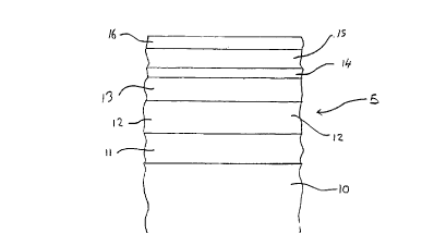
The typical structure of the HFETs tested is shown in Figure 1. The HFET
structures were grown by atmospheric pressure MOVPE using conventional methyl
metal group III and hydride group V precursors. The basic HFET structure 5,
grown on top of the buffer layer 11, lattice matched to a semi-insulating
AMENDED SHEET
CA 02193098 2000-OS-17 ~
8
iron-doped (100) InP substrate 10, consisted of the following layers: 0.3,um
undoped InP 12, 70nm S doped GaInAs (2x10'~cm~3 n-type) 13, 5nm undoped
GaAIAs 14, 50nm undoped AIInAs 15, 5nm undoped InP 16. The element ratios
should be those which give lattice matching to InP to ~ 1 OOOppm.
The HFETs were fabricated with 100,um wide, 1Nm long gates using the
process which is described in detail in D. J. Newson et al, "Damage-free
passivation of InAIAs/InGaAs HFETs by use of ECR-deposited SiN", Electronics
letters 1993, 29, pp472-474,
The results of the experimental pinch-off tests are correlated in Table 1.
The table also shows the conditions from which the results were derived. The
devices were designed to pinch-off fully before -2V gate bias. The criterion
used
in the table is pinch-off before -5V as such gross deviations are well outside
doping
control limits of the MOVPE kit used and must be substrate interface related.
The
first test approach (batches 1 to 9) was to load substrates as supplied
because
experience indicated that almost anything done to the Fe-doped material led to
poorer epilayer morphology. However, this approach, even when combined with a
variety of buffer layer types, only once led to good pinch-off (batch 6), and
this
was not reproducible.
In every case, when wafers or corresponding test structures from this
series were electrochemical capacitance/voltage (CV) depth profiled, a large
interfacial n-type spike in the range 5x10'6 to 5x10" cm'3 was found, as shown
in
Figure 2 (solid line). This n-type spike was at a depth which corresponded to
the
substrate/epitaxial layer interface and was a good indication that parallel
conduction mechanisms, and hence poor pinch-off characteristics, arose from
this
spike.
AMENDED SHEET
2 ~ 9~~98 ..
9
BATCH BOULE SUBSTRATE BUFFER LAYER NUMBER NUMBE
PREPARATION TESTED R WITH
l GOOD
PINCH-
OFF
1 C NONE 0.3pm u-InP 5 0
2 K NONE 0.3pm u-InP 1 0
3 K NONE 0.lpm Fe-InP, 0.3pm u-InP3 0
4 K NONE 0.lwm u-AIInAs, 0.3Nm 1 0
u-InP
S NONE 0.lpm u-AIInAs, 0.3Nm 2 0
u-InP
6 S NONE 5nm u-GaInAs, 0.l,um u-AIInAs,2 1
0.3~rm u-InP
7 S NONE 5nm u-InP, 5nm u-GaInAs, 1 0
100nm u-AIInAs
8 S NONE 0.lpm Fe-InP, 0.3m u-InP 2 0
9 S NONE 0.4pm u-InP 1 0
S WET ETCH 0.lpm Fe-InP, 0.3wm u-InP5 3
11 S WET ETCH 0.lpm Fe-AIInAs, 0.3pm 1 1
u-InP
12 S ANNEAL 0.lum Fe-InP, 0.3um u-InP1 1
&
GAS ETCH
13 S ANNEAL 0.lNm Fe-AIInAs, 0.3pm 2 2
& Fe-InP, 0.3Nm u-InP
GAS ETCH
14 Z ANNEAL 0.lpm Fe-AIInAs, 0.3pm 1 1
& Fe-InP, 0.3pm u-InP
GAS ETCH
F ANNEAL 0.l~rm Fe-AIInAs, 0.3pm 1 1
Fe-InP, 0.3um u-InP
16 F ANNEAL 0.l~rm Fe-AIInAs, 0.3~rm 2 2
& Fe-InP, 0.3pm u-InP
GAS ETCH
Table 1: showing the pinch-off performance of various HFETs fabricated
on substrates prepared in various ways (u indicates undoped, Fe indicates
5 iron-doped)
Trials with InP test layers showed that a wet-etch which included a
bromine-methanol step, in combination with growth of a thin, semi-insulating
Fe-doped InP or AIInAs anti-spike layer, was capable, in most cases, of
10 substantially reducing or eliminating the CV n-type spike. When this was
put into
the HFET process (batches 10 and 1 1 ), a much higher success rate was
achieved,
4 out of 6 wafers. Unfortunately though, some failures were still obtained,
even
within a single substrate batch.
Trials with HFETs grown on substrates prepared according to the present
15 invention (batches 12 to 16) provided a 100% success rate. Substrate
interfacial
AhiEPVu~~ ~l i(:I:i
WO 96/00979 2 I 9 3 0 9 8 PCT/GB95/01541
Trials with HFETs grown on substrates prepared according to the present
invention (batches 12 to 16) provided a 100% success rate. Substrate
interfacial
layers thus grown were always semi-insulating or low n-type by CV profiler
(Figure
2, dashed line). Again, note that although batches 12 to 16 all used a gas
etch,
5 the invention does extend to the use of a wet or other type of etch.
Although one wafer proved good (batch 15) even without the etching
step, the reproducibility of this was not explored because the etching step is
thought to offer greater protection against the vagaries of substrate quality
(boule
Z was from a source reported to be particularly susceptible to parallel
conduction
10 problemsl.
Figure 3 shows a set of HFET characteristics obtained from HFETs
fabricated on substrates prepared by the method according to the present
invention. From the graph it can be seen that pinch-off occurs at less than
2V.
While the method of substrate preparation described above finds
particular application in the field of HFET fabrication on InP substrates, it
will be
apparent that the technique finds important application in the general field
of
semiconductor device fabrication. In particular, the method is not limited to
the
steps described above for fabricating a standard HFET. The method finds
application in the fabrication of other types of semiconductor devices such as
HEMTs (high electron mobility transistors) and optical devices such as lasers,
and
photo-detectors, or indeed any type of semiconductor device which requires
high
quality InP substrate preparation. Thus the precise details of layer
composition,
doping, thickness and of overall device dimensions are given by way of example
only. Other devices, whether HFETs or otherwise, according to the invention
will
typically have very different characteristics to that described above.
Nevertheless,
the application of the present invention to the fabrication of semiconductor
devices
will be clear to those skilled in the art.
REFERENCES
1. N.Pan et al.,"Low temperature InAIAs buffer layers using trimethylarsenic
and arsine by metalorganic chemical vapour deposition", Appl. Phys. Lett.,
1993,
63, pp3029-3031