Note: Descriptions are shown in the official language in which they were submitted.
219339
COATED ARTICLE
Field of the Invention
The instant invention is directed to protective multilayer
metallic coatings for metallic substrates.
Background of the Invention
It is currently the practice with various brass articles such
as lamps, trivets, candlesticks, door knobs and handles and the
Like to first buff and polish the surface of the article to a high
gloss and to then apply a protective organic coating, such as one
comprised of acrylics, urethanes, epoxies, and the like, onto this
polished surface. While this system is generally quite
satisfactory it has the drawback that the buffing and polishing
operation, particularly if the article is of a complex shape, is
labor intensive. Also, the known organic coatings are not always
as durable as desired, particularly in outdoor applications where
the articles they are exposed to the elements and ultraviolet
radiation. It would, therefore, be quite advantageous if brass
articles, or indeed other metallic articles, could be provided with
a coating which gave the article the appearance of highly polished
brass and also provided wear resistance and corrosion protection.
The present invention provides such a coating. .
Summary of the Invention
The present invention i's directed to a metallic substrate
having a multi-layer coating disposed or deposited on its surface.
More particularly, it is directed to a metallic substrate,
particularly brass, having deposited on its surface multiple
superposed metallic layers of certain specific types of metals or
CA 02193439 1999-11-24
68432-289
metal compounds or metal alloys. The coating is decorative and
protective, e.g., provides corrosion and wear resistance. The
coating can simulate the appearance of highly polished brass, i.e. has
a brass color tone. Thus, an article surface having the coating
thereon simulates a highly polished brass surface.
This invention relates to an article comprising a
metallic substrate having disposed on at least a portion of its
surface a multi-layer coating simulating brass comprising: a layer
comprised of semi-bright nickel over at least a portion of said
surface of said substrate; a layer comprised of bright nickel over
at least a portion of said layer comprised of semi-bright nickel; a
layer comprised of palladium over at least a portion of said layer
comprised of bright nickel; a layer comprised of ruthenium over at
least a portion of said layer comprised of palladium; a layer
comprised of zirconium or titanium over at least a portion of said
layer comprised of ruthenium; and a layer comprised of zirconium
compound or titanium compound over at least a portion of said layer
comprised of zirconium or titanium.
This invention also relates to an article comprising a
substrate having on at least a portion of its surface a coating
having a brass color and comprising a first layer comprised of
semi-bright nickel; a second layer on at least a portion of said
first layer comprised of bright nickel; a third layer on at least a
portion of said second Layer comprised of palladium; a fourth layer
on at least a portion of said third layer comprised of ruthenium; a
2
2193439
68432-289
fifth layer on at least a port ion of said fourth layer comprised of
zirconium; and a sixth layer on at least a portion of said fifth
layer comprised of a zirconium compound.
A first layer deposited directly on the surface of the
substrate is comprised of nickel. The first layer preferably
consists of two different nickel layers such as a semi-bright
nickel layer deposited directly on the surface of the substrate and
a bright nickel layer superimposed over the semi-bright nickel
layer. Disposed over the nickel layer is a layer comprised of
palladium. This palladium layer is thinner than the nickel layer.
Over the palladium layer is a layer comprised of ruthenium. Over
the ruthenium layer is a layer comprised of a non-precious
refractory metal such as zirconium, titanium, hafnium or tantalum,
preferably zirconium or titanium. A top layer comprised of a
zirconium compound, titanium compound, hafnium compound or tantalum
compound, preferably a titanium compound or a zirconium compound
such as zirconium nitride, is disposed over the refractory metal
layer, preferably zirconium layer.
The nickel, palladium and ruthenium layers are preferably
applied by electroplating. The refractory metal layer such as
zirconium layer and refractory metal compound layer such as
zirconium compound layer are applied by vapor deposition such as
sputter ion deposition.
2a
. . ~ i 93439
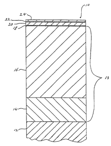
Brief Description of the Drawincts
FIG. 1 is a cross-sectional view of a portion of the substrate
having the multi-layer coating deposited on its surface.
Describtion of the Preferred Embodiment
The substrate 12 can be any metal or metallic alloy substrate
such as copper, steel, brass, tungsten, nickel alloys, and the
like. In a preferred embodiment the substrate is brass.
The nickel layer 13 is deposited on the surface of the
substrate 12 by conventional and well known electroplating
processes. These processes include using a conventional
electroplating bath such as, for example, a Watts bath as the
plating solution. Typically such baths contain nickel sulfate,
nickel chloride, and boric acid dissolved in water. Chloride,
sulfamate and fluoroborate plating solutions can also be used.
These baths can optionally include a number of well known and
conventionally used compounds such as leveling agents, brighteners,
and the like. To produce specularly bright nickel layer at least
one brightener from class I and at least one brightener from class
II is added to the plating solution. Class I brighteners are
organic compounds which contain sulfur. Class II brighteners are
organic compounds which do not contain sulfur. Class II
brighteners can also cause leveling and, when added to the plating
bath without the sulfur-containing class I brighteners, result in
semi-bright nickel deposits. These class I brighteners include
alkyl naphthalene and benzene sulfonic acids, the benzene and
naphthalene di- and trisulfonic acids, benzene and naphthalene
3
CA 02193439 1999-11-24
68432-289
sulfonamides, and sulfonamides such as saccharin, vinyl and allyl
sulfonamides and sulfonic acids. The class II brighteners
generally are unsaturated organic materials such as, for example,
acetylenic or ethylenic alcohols, ethoxylated and,propoxylated
acetylenic alcohols, coumarins, and aldehydes. These Class I and
Class II brighteners are well known to those skilled ~in the art and
are readily commercially available. They are described, inter
alia, in U.S. Patent No. 4,421,611.
The nickel lave= is preferably comprised of a duplex layer
cor_ta=ping a layer comer=sed of semi-bright nickel and a layer
comprised of bright n-ckel. The trickness of the nickel layer is
generally in the range of from about 100 millionths (0.000100) of
an inch, preferably about 150 millionths (0.000150) of an inch to
about 3,500 millior_ths (0.0035) of an inch.
As is well k_~_ow-~ i_~_ the art before the nickel 1 aver is
deoesited on tze subst=ate the substrate is subjected to said
activat=on by being placed in a conventional and well known acid
bath.
In a preferrec embodiment as illustrated in the FicLre, the
r_ickel layer 13 is comprised of two different nickel layers la anc
16. Layer le :s comprised of semi-bright nickel while layer 16 is
comps=sec of bric~.t r_i ckel . This duel ex r_ickel deposit provides
improved corrosion protection to the underlying substrate. The
semi-bright, sulfur-free plate 14 is deposited, by conventional
electroplating processes, directly on the surface of substrate 12.
4
. . 2 ~ 93439
The substrate 12 containing the semi-bright nickel layer 14 is then
placed in a bright nickel plating bath and the bright nickel layer
16 is deposited on the semi-bright nickel layer 14.
The thickness of the semi-bright nickel layer and the bright
nickel layer is a thickness effective to provide improved corrosion
protection. Generally, the thickness of the semi-bright nickel
layer is at least about 50 millionths (0.00005) of an inch,
preferably at least about 100 millionths (0.000100) of an inch, and
more preferably at least about 150 millionths (0.00015) of an inch.
The upper thickness limit is generally not critical and is governed
by secondary considerations such as cost. Generally, however, a
thickness of about 1,500 millionths (0.0015) of an inch, preferably
about 1,000 millionths (0.001) of an inch, and more. preferably
about 750 millionths (0.00075) of an inch should not be exceeded.
The bright nickel layer 16 generally has a thickness of at least
about 50 millionths (0.00005) of an inch, preferably at least about
125 millionths (0.000125) of an inch, and more preferably at least
about 250 millionths (0.000250) of an inch. The upper thickness
range of the bright nickel layer is not critical and is generally
controlled by considerations such as cost. Generally, however, a
thickness of about 2,500 millionths (0.0025) of an inch, preferably
about 2,000 millionths (0.002) of an inch, and more preferably
about 1,500 millionths (0.0015) of an inch should not be exceeded.
The bright nickel layer 16 also functions as a leveling layer which
tends to cover or fill in imperfections in the substrate.
CA 02193439 2000-10-13
68432-289
Disposed on the bright nickel layer 16 is a
relatively thin layer comprised of palladium. The palladium
strike layer 18 may be deposited on layer 16 by conventional
and well known palladium electroplating techniques. Thus for
example, the anode can be an inert platinized titanium while
the cathode is the substrate 12 having nickel layers 14 and 16
thereon. The palladium is present in the bath as a palladium
salt or complex ion. Such palladium baths are conventional and
well known. Some of the complexing agents include polyamines
such as described in U.S. Fatent No. 4,486,274. Some other
palladium complexes such as palladium tetra-amine complex used
as the source of palladium in a number of palladium
electroplating processes are described in U.S. Patent
Nos. 4,622,110; 4,552,628; and 4,628,165. Some palladium
electroplating processes are described in U.S. Patent
Nos. 4,487,665; 4,491,507 and 4,545,869.
The palladium strike layer 18 functions, inter alia,
as a primer layer to improve the adhesion of the ruthenium
layer 20 to the nickel layer, such as the bright nickel layer
16 in the embodiment illustrated in the Figure. This palladium
strike layer 18 has a thickness which is at least effective to
improve the adhesion of the ruthenium layer 20 to the nickel
layer. The palladium strike layer generally has a thickness of
at least about 0.25 millionths (0.00000025) of an inch,
preferably at least about 0.5 millionths (0.0000005) of an
inch, and more preferably at least about one millionth
(0.000001) of an inch. Generally, the upper range of thickness
is not critical and is determined by secondary considerations
such as cost. However, the thickness of the palladium strike
layer should generally not exceed about 50 millionths (0.00005)
of an inch, preferably 15 millionths (0.000015) of an inch, and
more preferably 10 millionths (0.000010) of an inch.
6
CA 02193439 2000-10-13
68432-289
The ruthenium layer 20 is deposited on the palladium
layer 18 in a variety of conventional and well known ways such
as for example by plating, sputtering, vacuum deposition, and
depositing the ruthenium metal as a finely divided dispersion
in an organic vehicle. The ruthenium is preferably deposited
by plating, preferably electroplating. The ruthenium
electroplating processes and plating baths are conventional and
well known. They are described, for example, in the Journal of
the Chemical Society of London, 1971 edition, page 839, by C.D.
Burke and J.O. O'Meardi and Electrodeposition of Alloys,
Vol. II, pp. 4-29, Abner Brenner (1963). The ruthenium
electroplating baths may be acidic or nonacidic. Some
illustrative examples of nonacidic ruthenium electroplating
baths are described in U.S. Patent Nos. 4,297,178 and
4,507,183. Some illustrative examples of acid ruthenium
plating baths are described in U.S. Patent No. 3,793,162. Some
other ruthenium plating baths are disclosed in U.S. Patent
Nos. 3,576,724 and 4,377,488. The ruthenium plating baths
include the nitrous salt baths and the sulfamate baths.
The ruthenium may be electroplated by use of
continuous direct current densities or by use of pulse current
plating, i.e., where a current is generated for a first time
period and is absent during a second time period, the first and
second time period reoccur cyclically. Pulse current plating
of ruthenium is described, for example, in U.S. Patent
No. 4,082,622.
The thickness of the ruthenium layer 20 is at least
about 2 millionths (0.000002) of an inch, preferably at least
about 5 millionths (0.000005) of an inch, and more preferably
at least about 8 millionths (0.000008) of an inch. The upper
thickness range is not critical and is generally dependent on
7
CA 02193439 2000-10-13
68432-289
economic considerations. Generally, a thickness of about 100
millionths (0.0001) of an inch, preferably about 75 millionths
(0.000075), and more preferably about 50 millionths (0.00005)
of an inch should not be exceeded.
Disposed over the ruthenium layer 20 is a layer 22
comprised of a non-precious refractory metal such as hafnium,
tantalum, zirconium or titanium, preferably zirconium or
titanium, and more preferably zirconium.
Layer 20 serves, inter alia, to improve or enhance
the adhesion of layer 24 to layer 20. Layer 22 is deposited on
the ruthenium layer 20 by conventional and well known
techniques such as vacuum coating, physical vapor deposition
such as ion sputtering, and the like. Ion sputtering
techniques and equipment are disclosed, inter alia, in
T. Van Vorous, "Planar Magnetron Sputtering; A New Industrial
Coating Technique", Solid State Technology, Dec. 1976,
pp 62-66; U. Kapacz and S. Schulz, "Industrial Application of
Decorative Coatings - Principle and Advantages of the Sputter
Ion Plating Process", Soc. Vac. Coat., Proc. 34th Arn. Techn.
Conf., Philadelphia, U.S.A., 1991, 48-61; and U.S. Patent
Nos. 4,162,954, and 4,591,418.
Briefly, in the sputter ion deposition process the
refractory metal such as titanium or zirconium target, which is
the cathode, and the substrate are placed in a vacuum chamber.
The air in the chamber is evacuated to produce vacuum
conditions in the chamber. An inert gas, such as Argon, is
introduced into the chamber. The gas particles are ionized and
are accelerated to the target to dislodge titanium or zirconium
atoms. The dislodged target material is then typically
deposited as a coating film on the substrate.
8
CA 02193439 2000-10-13
68432-289 '
Layer 22 has a thickness which is at least effective
to improve the adhesion of layer 24 to layer 20. Generally,
this thickness is at least about 0.25 millionths (0.00000025)
of an inch, preferably at least about 0.5 millionths
(0.0000005) of an inch, and more preferably at least about one
millionth (0.000001) of an inch. The upper thickness range is
not critical and is generally dependent upon considerations
such as cost. Generally, however, layer 22 should not be
thicker than about 50 millionths
9
2193439
(0.00005) of an inch, preferably about 15 millionths (0.000015) of
an inch, and more preferably about 10 millionths (0.000010) of an
inch.
In a preferred embodiment of the present invention layer 22 is
comprised of titanium or zirconium, preferably zirconium, and is
deposited by sputter ion plating.
Layer 24 is comprised of a hafnium compound, a tantalum
compound, a titanium compound or a zirconium compound, preferably
a titanium compound or a zirconium compound, and more preferably a
zirconium compound. The titanium compound is selected from
titanium nitride, titanium carbide, and titanium carbonitride, with
titanium nitride being preferred. The zirconium compound is
selected from zirconium nitride, zirconium carbonitride, and
zirconium carbide, with zirconium nitride being preferred.
Layer 24 provides wear and abrasion resistance and the desired
color or appearance, such as for example, polished brass. Layer 24
is deposited on layer 22 by any of the well known and conventional
plating or deposition processes such as vacuum coating, reactive
sputter ion plating, and the like. The preferred method is
reactive ion sputter plating.
Reactive ion sputter is generally similar to ion sputter
deposition except that a reactive gas which reacts with the
dislodged target material is introduced into the chamber. Thus, in
the case where zirconium nitride is the top layer 24, the target is
comprised of zirconium and nitrogen gas is the, reactive gas
introduced into the chamber. By controlling the amount of nitrogen
2 i 9.3439
available to react with the zirconium, the color of the zirconium
nitride can be made to be similar to that of brass of various hues.
Layer 24 has a thickness at least effective to provide
abrasion resistance. Generally, this thickness is at Least 2
millionths (0.000002) of an inch, preferably at least 4 millionths
(0.000004) of an inch, and more preferably at least 6 millionths
(0.000006) of an inch. The upper thickness range is generally not
critical and is dependent upon considerations Such as cost.
Generally a thickness of about 30 millionths (0.00003) of an inch,
preferably about 25 millionths (0.000025) of an inch, and more
preferably about 20 millionths (0.000020) of an inch should not be
exceeded.
Zirconium nitride is the preferred coating material as it most
closely provides the appearance of polished brass.
In order that the invention may be more readily understood the
following example is provided. The example is illustrative and
does not limit the invention thereto.
EXAMPLE 1
Brass door escutcheons are placed in a conventional soak
cleaner bath containing the standard and well known soaps,
detergents, defloculants and the like which is maintained at a pH
of 8.9 - 9.2 and a temperature of 180 - 200oF for 30 minutes. The
brass escutcheons are then placed for six minutes in a conventional
ultrasonic alkaline cleaner bath. The ultrasonic cleaner bath has
a pH of 8.9 - 9.2, is maintained at a temperature of about 160 -
180oF, and contains. the conventional and well known soaps,
11
2193439
detergents, defloculants and the like. After the ultrasonic
cleaning the escutcheons are rinsed and placed in a conventional
alkaline electro cleaner bath for about two minutes. The electro
cleaner bath contains an insoluble submerged steel anode, is
maintained at a temperature of about 140 - 180oF, a pH of about
10.5 - 11.5, and contains standard and conventional detergents.
The escutcheons are then rinsed twice and placed in a conventional
acid activator bath for about one minute. The acid activator bath
has a pH of about 2.0 - 3.0, is at an ambient temperature, and
contains a sodium fluoride based acid salt. The escutcheons are
then rinsed twice and placed in a semi-bright nickel plating bath
for about 10 minutes. The semi-bright nickel bath is a
conventional and well known bath which has a pH of about 4.2 - 4.6,
is maintained at a temperature of about 130 - 150oF, contains
NiS04, NiCL2, boric acid, and brighteners. A semi-bright nickel
layer of an average thickness of about 250 millionths of an inch
(0.00025) is deposited on the surface of the escutcheon.
The escutcheons containing the layer of semi-bright nickel are
then rinsed twice and placed in a bright nickel plating bath for
about 24 minutes. The bright nickel bath is generally a
conventional bath which is maintained at a temperature of about 130
- 150oF, a pH of about 4.0 - 4.8, contains NiS04, NiCL2, boric acid,
and brighteners. A bright nickel layer of an average thickness of
about 750 millionths (0.00075) of an inch is deposited on the semi-
bright nickel layer. The semi-bright and bright nickel plated
escutcheons are rinsed three times and placed for about one and a
12
2 ~ 93439
half minutes in a conventional palladium plating bath. The
palladium bath utilizes an insoluble platinized niobium anode, is
maintained at a temperature of about 95 - 140oF, a pH of about 3.7
- 4.5, contains from about 1-5 grams per liter of palladium (as
metal), and about 50-100 grams per liter of sodium chloride. A
palladium layer of an average thickness of about three millionths
(0.000003) of an inch is deposited on the bright nickel layer. The
palladium plated escutcheons are then rinsed twice.
The palladium plated escutcheons are then placed into a
conventional ruthenium plating bath for about ten minutes. The
ruthenium.bath utilizes insoluble platinized titanium anodes, is
maintained at a temperature of about 150-170 deg F, a pH of about
1.0-2.0, and contains about 3 grams per liter of ruthenium. A
ruthenium layer of an average thickness of about 10 millionths of
an inch is deposited over the palladium layer. The escutcheons are
then thoroughly rinsed and dried.
The ruthenium plated escutcheons are placed in a sputter ion
plating vessel. This vessel is a stainless steel vacuum vessel
marketed by Leybold A.G. of Germany. The vessel ~i.s generally a
cylindrical enclosure containing a vacuum chamber which is adapted
to be evacuated by means of pumps. A source of argon gas is
connected to the chamber by an adjustable valve for varying the
rate of flow of argon into the chamber. In addition, two sources
of nitrogen gas are connected to the chamber by an adjustable valve
for varying the rate of flow of nitrogen into the chamber.
13
2 ~ 93439
Two pairs of magnetron-type target assemblies are mounted in
a spaced apart relationship in the chamber and connected to
negative outputs of variable D.C. power supplies. The targets
constitute cathodes and the chamber wall is an anode common to the
target cathodes. The target material comprises zirconium.
A substrate carrier which carries the substrates, i.e.,
escutcheons, is provided, e.g., it may be suspended from the top of
the chamber, and is rotated by a variable speed motor to carry the
substrates between each pair of magnetron target assemblies. The
carrier is conductive and is electrically connected to the negative
output of a variable D.C. power supply.
The ruthenium plated escutcheons are mounted onto the
substrate carrier in the sputter ion plating vessel. The vacuum
chamber is evacuated to a pressure of about 5x10⁻³ millibar and is
heated to about 400oC via a radiative electric resistance heater.
The target material is sputter cleaned to remove contaminants from
its surface. Sputter cleaning is carried out for about one half
minute by applying power to the cathodes sufficient to achieve a
current flow of about 18 amps and introducing argon gas at the rate
of about 200 standard cubic centimeters per minute. A pressure of
about 3x10⁻³ millibars is maintained during sputter cleaning.
The escutcheons are then cleaned by a low pressure etch
process. The low pressure etch process is carried on for about
five minutes and involves applying a negative D.C. potential which
increases over a one minute period from about 1200 to about 1400
volts to the escutcheons and applying D.C. power to the cathodes to
14
2 i 93439
achieve a current flow-of about 3.6 amps. Argon gas is introduced
at a rate which increases over a one minute period from about 800
to about 1000 standard cubic centimeters per minute, and the
pressure is maintained at about 1.1x10⁻² millibars. The escutcheons
are rotated between the magnetron target assemblies at a rate of
one revolution per minute. The escutcheons are then subjected to
a high pressure etch cleaning process for about 15 minutes. In the
high pressure etch process argon gas is introduced into the vacuum
chamber at a rate which increases over a 10 minute period from
about 500 to 650 standard cubic centimeters per minute (i.e., at
the beginning the flow rate is 500 sccm and after ten minutes the
flow rate is 650 sccm and remains 650 sccm during the remainder of
the high pressure etch process), the pressure is maintained at
about_2x10-1 millibars, and a negative potential which increases
over a ten minute period from about 1400 to 2000 volts is applied
to the escutcheons. The escutcheons are rotated between the
magnetron target assemblies at about one revolution per minute.
The pressure in the vessel is maintained at about 2x10⁻¹ millibar.
The escutcheons are then subjected to another low pressure
etch cleaning process for about five minutes. During this low
pressure etch cleaning process a negative potential of about 1400
volts is applied to the escutcheons, D.C. power is applied to the
cathodes to achieve a current flow of about 2.6 amps, and argon gas
is introduced into the vacuum chamber at a rate which increases
over a five minute period from about 800 sccm (standard cubic
centimeters per minute) to about 1000 sccm. The pressure is
21 93439
maintained at about 1.1x10⁻² millibar and the escutcheons are
rotated at about one rpm.
The target material is again sputter cleaned for about one
minute by applying power to the cathodes sufficient to achieve a
current flow of about 18 amps, introducing argon gas at a rate of
about 150 sccm, and maintaining a pressure of about 3x10⁻³
millibars.
During the cleaning process shields are interposed between the
escutcheons and the magnetron target assemblies to prevent
deposition of the target material onto the escutcheons.
The shields are removed and a layer of zirconium having an
average thickness of about 3 millionths (0.000003) of an inch is
deposited on the ruthenium layer of the escutcheons during a four
minute period. This sputter deposition process comprises applying
D.C. power to the cathodes to achieve a current flow of about 18
amps, introducing argon gas into the vessel at about 450 sccm,
maintaining the pressure in the vessel at about 6x10-' millibar, and
rotating the escutcheons at about 0.7 revolutions per minute.
After the zirconium layer is deposited a zirconium nitride
layer having an average thickness of about 14 millionths (0.000014)
of an inch is deposited on the zirconium laKer by reactive ion
sputtering over a 14 minute period. A negative potential of about
200 volts D.C. is applied to the escutcheons while D.C. power is
applied to the cathodes to achieve a current flow of-about 18 amps.
Argon gas is introduced at a flow rate of about 500 sccm. Nitrogen
gas is introduced into the vessel from two sources. One source
16
2193439
introduces nitrogen at a generally steady flow rate of about 40
sccm. The other source is variable. The variable source is
regulated so as to maintain a partial ion current of 6.3x10'11 amps,
with the variable flow of nitrogen being increased or decreased as
necessary to maintain the partial ion current at this predetermined
value.
The pressure in the vessel is maintained at about 7.5x10⁻³
millibar.
The zirconium-nitride coated escutcheons are then subjected to
low pressure cool down, where the heating is discontinued, pressure
is increased from about 1:1x10-Z inillibar to about 2x10⁻¹ millibar,
and argon gas is introduced at a rate of 950 sccm.
Although the present invention has been described in
conjunction with preferred embodiments, it is to be understood that
modifications and variations may be resorted to without departing
from the spirit and scope of the invention, as those skilled in the
art will readily understand. Such modifications and variations are
considered to be within the purview and scope of the invention and
appended claims.
17