Note: Descriptions are shown in the official language in which they were submitted.
WO 95127931 PCT/US95103856
2~ 9~47~
GOAD TAP CHANiGER
B~ckarouad of the Tavention
This invention relates to tap changers
for electrical inductive equi~gment. Tap
changing is used extensively in a wide variety
of electrical inductive apparatus such as AC
voltage regulating tranaforme:rs, HVDC rectifier
and inverter transfo»ers and phase angle
regulators to adjust the devices turns ratio or
phase angle while the device is serving load.
Most of the tap changing mathada in use utilize
a switching means to alternately connect various
sections of one winding of the electrical
inductive apparatus i.ato s circuit. One
extensively used switching means is a mechanical
contact switch is which a movable contact
selectively engages stationary contacts
connected to various sections of the winding so
as to connect varying numbers of turns into the
circuit. Thin methodology is at present used to
the virtual exclusion of all other methods in
large power apparatus.
Another type of switching mesas, which
has been the subject o'f patents activity and
technical papers with increasing frequency due
to its fast response time and lack of mechanical
wear, is the electronic switch. Electronic
WO 95127931 PCT/HJS951Q3856
~f93477
F..'1 ~ . _
switches are typically electronically controlled
gate devices, such as thyriators and gate tuna
off devices, which are connected as an inverse
parallel-connected pair to each tap of a
winding, as shown is V.S. patent 3,195,038. A
control device triggers predetermined gsoups,of
the thyriator pairs to connect or bypass certain
ones of the tap winding sections and thereby
provide a range of individual output voltage
increments for an electrical inductive
apparatus. The total number of discrete voltage
increments may be extended, as shown in the
above referenced patent, by utilising additional
thyristor pairs with each winding section to
reconfigure the relative polarity of the winding
sections and thereby dispose each winding
section in additive or opposing relation with
the remainder of the winding sections. Further,
tapped secondary windings may be utilized with
appropriate switching devices to increase the
tap range of the electrical inductive apparatus
as shown in U.S. patents 3,195,038, 3,909,697,
Bad 81x0 3,700,925.
Several of the prime considerations
affecting economical usage of solid-state tap
changers in electrical inductive apparatus are
the total number of electrical switches, their
individual ratings, their associated losses, and
the number of individual winding sections within
the inductive device required to provide a
predetermined number of output voltage
increments within the total output voltage range
of the electrical inductive apparatus.
Obviously, the cost of the tap changer mechanism
may be reduced if fewer thyriator switches of
lower rating are used with a simpler winding
configuration. Prior art electronic tap
W095/27931 PCT/U595103856
_ 3 _
changing arrangements have ceL~tain drawbacks
regarding these conai.deratioaa since they
require an excessive number of switches and
individual winding sections to provide a large
number of discrete output voltage increments
required in commercial applications of such
electrical inductive apparatus. Due to the
extreme cost none of the proposed arrangements
for controllable electronic tap changers were at
any time placed into commercial operation in
large power equipment.
Efforts have been made to address this
uneconomical condition with the use of phase
control, as taught in U.S. patent 4,220,911, but
this configuration produces urnacceptably high
levels of harmonics sad as such is unacceptable
practically since filters or ether methods of
mitigating the effect of these parasitic
harmonics must be used. Other approaches, such
as those described in U.S. patents 4,135,126,
3,786,337, 3,319,153, 3,600,664, 3,684,949, and
3,461,378 have likewise not proved satisfactory.
At present there is still no commercially viable
arrangement, of any form, that makes the solid-
state tap changer economically attractive for
commercial use.
Thus, it is desirable to provide an
electrical inductive apparatus which has as
improved tap changing means which provides a
commercially acceptable number of output voltage
increments through the use of a reduced number
of individual switch devices having lower
ratings, a simpler sad less costly tap winding
structure, and a control logic which makes the
moat efficient use of the ratings of the
electronic components.
Aa objective of the present invention
WO 95/27931 PCTlUS95103856
,,.f; : ~.~; ~ ~ 9 3 4 71
:.r~..,
is to provide s completely son mechanical
contact switching device having a high speed of
response and high reliability, ae well as
economical cost. Another objective of the
invention is to provide reliable operation and
switching independent of the nature of the load
at any moment is time. Another objective of the
invention is to provide reliable switching
action between any two tap settings including
switching taps sequentially or selectively over
the entice tap range. It is also the objective
of this invention to design the control so that
the switch can be operated such that the output
RMS voltage is controllable and selectable
between the distinct voltage increments dictated
by the winding configuration. Aa additional
objective of this invention is to use the switch
as a device to limit the duration of the fault
current through the apparatus and the switch
itself so that the device rating and coat of the
device be reduced significantly.
Summary of the Invention
Accordingly it is the primary object
of_thie invention to provide a load tap changer
which achieves the stated objectives and is
economical to construct. This is accomplished
by reducing the number and required rating of
the controllable electronic devices required to
provide the desired voltages.
This and other objects of the
invention are achieved, in accordance with one
aspect of the invention by a tap changing system .
for operation with an inductive device, and
including a reference potential comprising:
a tap changer winding having opposite
ends and a plurality of tap winding sections,
having upper and lower end points, serially
WO 95127931 PCTIUS95/03856
;.. ; ;~; ~;~;; ~., i .,~.
,. ~T 93477
- 5 -
connected with said inductive device and said
reference potential;
individual first groups of gate-
controlled electronic devices, having one and
another end, connected between said end points
' on the respective tap winding sections and said
reference potential;
a separate, second group of gate-
controlled electronic devices coanectad directly
to one end of said first groups of gate-
coatrolled electronic devices and to reference
potential, said second group being more highly
rated than said first groug of gate-controlled
electronic devices, said second group
functioning normally in the ON-state;
said separate, second group acting as
a circuit breaker under over-current conditions
such that, within one-half cycle thereof, said
second group is transferred to the OFF-state,
whereby said tap changer wiad.ing is open
circuited;
a control means for providing control
signals to each of the respective gates of said
gate-controlled electronic devices to control
the states of combination of said devices.
Another aspect of the invention
includes a tap changer system comprising:
an inductive device connected to a
load;
a plurality of switches connected to
said inductive device and to an associated
plurality of physical tap windings in the
controlled configuration;
control means for e:electing
combinations of said switches: to be gated into
conducting states; and
means for gating such combinations on
WO 95127931 PCT/US95103856
.,
:.~,~n~;;~...~:~ ~ 193471
.,~,d.; ..,:
-6-
a time-sharing basis such that predetermined
ones of said switches sad their associated
physical tap windings will be conducting for
selected time periods, such that tap voltage
magnitudes are produced in increments
intermediate said physical tap winding voltage
magnitudes.
A further aspect of the invention
comprises a load tap changer system for
minimizing perceptible flicker comprising:
an inductive device connected to a
load;
a plurality of switches connected to
said inductive device and having a plurality of
physical tap windings in a controlled
configuration connected to said device;
control means for selecting
combination of said switches to be gated into
conducting states;
mesas for gating such combinations oa
a time-sharing basis such that say one or mose
of said switches will be conducting for selected
time periods, whereby tap voltage values are
obtainable is increments between the physical
tap winding voltage magnitudes; and
mesas for providing discrete cycle
modulation packets, said packets comprising a
first discrete cumber of cycles of one magnitude
of output tap voltage, and a second discrete
number of cycles at another output tap voltage
magnitude, said total number of voltage cycles
when switched producing an effective output tap
voltage which is the average of the individual
output-tap voltages resulting from said first ,
and second discrete number of cycles of
different voltage magnitudes, where N is total
number of cycles in a modulation packet, M is
CA 02193477 1999-09-10
_ 7 _
the number of cycles at the higher voltage, Vo is said
one voltage magnitude and V1 is said another voltage
magnitude.
Yet another aspect of the invention includes
a tap changer winding-switching configuration
comprising:
at least three pairs of gate-controlled
devices coupled in parallel, said pairs having
respective first, second and third common nodes, within
each pair each common node being disposed between the
gate-controlled devices of said pair;
a first tap winding, having a first voltage
magnitude, connected between said first and second
common nodes, and a second tap winding, having a second
value, connected between said second and third common
nodes;
control means for switching said switching
devices to select any one of said tap windings in
additive and subtractive combination thereof.
Brief Description of Drawings
Figure 1. Depicts a tap changer of the prior
art having a standard tap winding arrangement with
fully rated thyristors to address the short-circuit
duty of the transformer. This Figure also illustrates
the tap winding reversing arrangement accomplished with
thyristors.
Figure 2. Depicts a configuration in
accordance with the present invention, featuring a
specially chosen second group of controllable
electronic devices functioning as a circuit breaker.
Figure 3. Depicts another configuration in
accordance with the present invention, but requiring
fewer groups of
R'O 95127931 ~ ~ ~ PC~ 595103856
,Y '~. ~.~4: E': . ~>
,: 1 .
8 _
controllable electronic devices for the number
of tap changer steps required.
Figure 4. Depicts another version of
Figure 3 with non-linear resistors MOV (metal
oxide varistors? used to protect the system
during transient overvoltage and grading
resistors to help distribute the open circuit
voltage in a desired manner.
Figure 5. Depicts a possible
arrsagament for voltage grading during the
period after the tap changer mechanism has been
open circuited.
Figure 6. Depicts one of the several
possible variations of the configuration
illustrated in Figure 3.
Figure 7. Depicts a possible
arrangement to shoat the short circuit current
through a load.
Figure 8A, 8B, & 8C. Depict the first
three geometric tap winding arrangements taught
is accordance with this invention.
Figure 9. Is a schematic diagram of a
single phase circuit topology involving a plus
or minus 10% load tap changer, having a minimum
of 32 incremental tap voltage steps, three
physical tap windings being located with the
transformer winding, on a 34.5 KV 30 MVA system
using 4500 volt SCRs; further including a
control device shown in simplified form for
controlling transmission of switching signals to
the gates of the individual switches.
Figure 10A. Is a block diagram of a .
first embodiment showing the components inside
the control device 20", such components being ,
arranged to provide gate signals for purposes to
be described.
Figure lOB. Is another block diagram
CA 02193477 1999-09-10
- 9 -
of a second embodiment, which is similar to Figure 10A.
Figure 11. . Is a flow chart of DCM control
software operative in accordance with the present
invention.
Figure 12. Is a graph of the output voltage
vs. time.
Figure 13. Is a schematic diagram of an
alternate embodiment of a single phase circuit
topology, as in Figure 9, having a plus or minus 10~
load tap changer; but applied on a 115 KV, 100 MVA
system using 4500 V SCRs.
Description of Preferred Embodiments
Before proceeding with the description of the
preferred embodiments, reference shall first be made to
Figure 1 in which a solid state tap changer 10
involving the use of groups of thyristor devices is
illustrated. This is the solid state tap changer
constituting an extension or enhancement of the
previously mentioned mechanical load tap changer which
was described in detail in patent 3, 195, 038 (U. S .
patent to Fry).
It should be noted in Figure 1, that
thyristor pairs A and B are so connected that they
allow reversing of the turns in the tap winding; that
is to say, turns can be added or subtracted by current
flow in respectively opposite directions. Accordingly,
if zero additional turns were desired, thyristor groups
B and C would have control signals sent from control
device 20 to the gates of the back-to-back pair of
thyristors in each of the blocks designated B and C.
As can be understood, current would flow through the
thyristors in the groups B and C and thence to
reference potential (ground) in the tap changer 10. To
add a single tap the control device (20) would send
gating
WO 95/27931 PCTlUS95103856
~~tr~.
'~ ~ ~ c.. ~ ~ _,
~~~3477
- to -
signals to thyriator groups B and D. To obtain
a reduction of a single tap the control would
apply control signals to the thyriator groups A
and R. Ccrrespoadiagly, for subtracting two
tape (windings shown having a value of 1)
thyriator pairs A sad Q would be provided
control signals, sad for subtracting three taps,
it would be groups A and P, etc.
As will be appreciated, the control
device 20 functions responsive to input control
line 22, to provide the control signals to the
gates of the thyristor back-to-back pair groups
A-5 at the proper time to accomplish the desired
tunas ratio. In the particular showing of
Figure 1, the control is accomplished
electrinally by extending the output control
lines A-S, seen on the left side of control
device 20, to the respective gates of each
thyristor pair of the groups. This effect can
also be accomplished optically or by other
suitable means.
Coaventional power systems tap
changers are normally designed for plus or minus
16 steps or taps with each tap step being
approximately 5/8~. If this is the assumed
arrangement for the tap changer 10 is Figure l,
then 19 back-to-back thyristor pairs would be
required. Each of these 19 pairs would have to
be rated for the full short-circuit current the
system would deliver when limited only by the
impedance of the inductive device. From this it
will be appreciated that the cost of this ,
conveatioaal configuration or arrangement is
substantial since each of the thyristors has to ,
be rated to carry the short-circuit current
limited -only by the impedance of the transformer
for the length of time dictated by ANSI
WO 95/27931 PCTlUS95103856
,. ? fi 93477
- 11 -
standards. This is very complex, but, in
general, class III transformers may be required
to withstand a fully offset short-circuit
current for at least 1 second. Users can and do
specify other duties including 1 second oa, x
seconds off, sad 1 second on again.
It will be understood that, although
the Figure 1 embodiment shows a transformer, and
reference will be made hereinafter to
transformers, that other types of inductive
devices, such as voltage or current regulations
and the like, can be utilized with the present
invention.
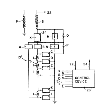
Ia contrast to the prior art shown in
Figure 1, Figure 2 represents a preferred
embodiment of the present invention, which
involves limiting the current through the tap
changing mechanism during short-circuit fault by
the addition of another controllable electronic
device; that is, a separate second group of
thyristors. Figure 2 is similar to Figure 1 in
that the tap windings are connected to the main
windings of the transformer with controllable
electronic switches and these switches are
activated with a control (20') analogous to
control device (20) in Figures 1. However, the
additional group of controllable electronic
devices, group X, has been added between the tap
winding T and the main winding S. This
additional group of controllable electronic
switches is controlled so that after a
~ predetermined high level of fault over-current
is detected by input control line 22 connected
to control device 20' from the transformer
secondary S, group X is gated off by means of
output control line 24 from control device 20'
to the gates of the croup X thyristors. The
R'O 95/27931 PCTlUS95103856
293477
- 12 -
term "over-current" is used herein to denote a
level of current approaching a full short
circuit condition.
Group X can take the form of a normal
thyristor which stops conducting at the next
current zero after gating signals are stopped
or, alternately, a gate turnoff device which
forces the current to zero based upon some
control logic. As an example, if during a fault
the current through the apparatus sad tap
windings reach a level deemed too large, the
gating signal to group X is interrupted and at
the next current zero the thyristor stops
passing current.
Alternately, the device using a GTO~s
(gated tuna off devices) can be used to force
the current to zero at any time within the half-
cycle during which the current through the tap
wiading(s) exceeds preset limits. Fault
duration in this embodiment is limited to the
speed with which the over-current can be
detected and the required signal can be
delivered to the control. Oae skilled is the
art will recognize that the GTO controlled
device can also be gated appropriately to
commutate the power flow is one or all of the
windings, allowing the transformer to remain on
line during a fault or transient overload
condition until the system control provides a
signal to gate it off line or the transient
overload condition is over.
The effect of this is to open circuit
the apparatus secondary winding "S" sad to limit
the short-circuit current after the first half-
cycle to zero. The voltage across electronic
device X is then determined by the winding and
the type of fault encountered sad the system X/R
WO 95/27931 PCTIUS95103856
'.~ ~. : ,~ ; ,,.. ~ 19 3 4 7 l
yi:~ .:i ..J
- 13 -
ratio (reactance to resistaac~e ratio).
Consequently, the breaker controllable
electronic switch group X, must be rated to
withstand the subsequent open circuit voltage of
the secondary winding. This, however, is a more
economical arrangement than Mast of ensuring
that all controllable electronic switches in the
tap arrangement can carry the fault current for
the full length of the system fault.
Ia Figure 2 group X is located between
the secondary winding and the tap winding. Thie
additional controllable electronic group may
also be located at the line end, the neutral, or
distributed throughout the tap winding itself.
The selection of its location will not affect
its stated function, which is to provide a
method to allow the reduction of the rating of
the controllable electronic switches in the tap
changing mechanism. Figure 2 illustrates a
solidly grounded winding but the method
presented hare applies equall~r well to a delta
winding and other windings of more complex
configuration.
Resistors O and P are included in the
circuit for the purpose of helping to grade (or
distribute in a desired manner) the open circuit
voltage across the.coatrollable electronic
devices X, A, B, C, etc., so that the most
affective use of the controllable electronic
switches voltage characteristic can be made.
Although not shown, electronic protective
circuits such as VBO (voltage break over) or MOV
(metal oxide varistore) can be used to protect
the system for unusually high transient or
dynamic voltages.
It will be understood by those versed
is the art that one clear advantage of Figure 2
WO 95127931 PCT/OS95103856
~~y' ''~ i, ~~ ~ ~ ~ y3
- 14 - 2~g3477
over that of Figure 1 is that the controllable
electronic switches is the tap changing winding
of Figure 2 can be of considerably lower current
rating. Accordingly, the cost of the tap
changing device or system can be reduced
considerably. Additionally, group X can replace
the system breaker and thn reclosing mechanisms
for that particular apparatus, since, group X
must be rated for full load current and is
capable of reacting faster (at least one half-
cycle) than any mechanical brnaker.
As will be understood from what has
been indicated previously, the function of the
control device 20' is to provide the gating
signals to the controllable electronic devices
to accomplish at least three activities: the
selection of the appropriate electronic devices
to achieve the desired voltage or current level
(elements A-I. is Figure 2); to gate or block the
breaker (group X in Figure 2); and to protect
the system due to failure of the control itself
or some component in the apparatus or system.
Current state of the art in gating of
controllable elnctroaic devices is sufficient to
meet any envisioned control and/or protection
strategy.
Figure 3 illustrates a different
winding arrangement from those shown is Figure 1
and 2. Figure 3, like Figure 2, combines a tap
changing mechanism with the circuit opening (or
breakerD controlled electronic device. Thin
will accomplish the desired task of controlling ,
the flow of short-circuit current sad allowing
lower rated electronic devices to be reliably
used. Figure 3 also shows a subset of a
geometric winding arrangement which requires the
minimum number of controllable electronic
WO 95/27931 PCTlOS9510385G
.,-~ ~,~,~x~_; ~ 193477
- 15 -
devices to achieve the desired voltage steps.
With this illustrated subset arrangement, there
are 2 tap winding groups, the first group 12
being indicated to have sections of one unit
each and the other group 14 to the right of the
first group, having sections of 4 units each.
It is understood that each unit may consist of
one or more winding turns based oa the turns
ratio of the device to which it is applied.
Thus, the tap winding group to the right is what
may also be termed the second group has a number
of turns 4 times greater than the number of
turns in each of the sections is the group 12,
or first spaced group.
Figure 8 contains three geometric tap
winding arrangements requiring the minimum
number of controllable electronic switches for
the maximum number of integer tap steps. Figure
8A contains the simplest arrangement comprised
of two one step taps and one two step tap. With
8 thyristora (or controllable electronic
switches) this arrangement can achieve up to
plus or minus 4 tap steps. Figure 8B contains
the next geometric arrangement which is 3 groups
of one step taps, 2 groups of three step taps,
and 1 group of sine step taps. As shows with
the use of 12 pairs of thyriators this
arrangement can achieve up to plus or minus 18
steps. Figure 8C illustrates a geometric tap
arrangement of 4 groups of one step tap, 3
groups of four step taps, 2 groups of 16 step
. taps, and 1 group of a 48 step tap. With 17
thyristors this arrangement can achieve every
integer step from -96 to +96. Figure 3 contains
a tap winding arrangement which consists of the
first two tap winding groups of Figure 8C. The
advantage of this type of tap winding
WO 95127931 PC'TlUS95l03856
X193477
- 16 -
arrangement is the simplicity of winding
construction and the reduced number of required
controllable electronic switches to achieve a
desired voltage level (in this example the
industry standard of + and - 16 steps).
Accordingly, this arrangement will produce as
electronic tap changing mechanism of reduced
cost.
It should be noted in connection with
Figure 3, that the control device previously
seen has been eliminated for the purpose of
simplification. Also, the non-linear resistors
(MOV's) N and M seen is Figure 2, and voltage
grading resistors O and P have been eliminated
for clarity in the drawing but may be required
in the construction.
In Figure 3, under the aasumptioa of
normal operation, the control device will gate
(fire) the appropriate thyriators (or
controllable electronic switches) to select the
specified tap position. Such normal operation
will be referred to as mode 1. It will be seen
that for the case of zero added turns to the
secondary-the current path will involve current
flow through either the path containing
thyristora X, R, and L in aeries or X, A, and B
in series. As will be apparent such current
flow is to reference potential (ground). The
other positions, involving steps 1 through plus
16 or minus 1 through minus 16 involve two
possible cries-cross paths in Figure 3. The
flow for negative taps is through R and thence
through various selected paths, including any
one of C to F and G to J and finally B to
ground. The flow for positive tap addition is
through A sad then say controllable switch C to
F and G to J sad finally L to ground.
W095/27931 PCT'1US95103856
~ ~ ~~ ~; ;~' ~7 ~ ~} a '19 3 4 7 7
-1~-
As one example, let us assume that one
wants plus 7 winding taps at a given moment,
then controllable electronic switches X, A, E,
H, and L are selected as those is the group of
thyristors that are to be gated oa and
conducting. The E group is at a location, i.e.,
the left leg, for which current flow is in the
plus direction through three single tap units,
and H involves current flow also is the plus
direction through four units in the leg on the
right. Accordingly, the total added tap winding
sections is plus 7.
The person versed in the art will
understand the other possible combinations that
may be selected (34 possible integer positions
being selectable, two of which have the same
tunas value).
One of the primary concerns is the
design of a device which contains controllable
electronic switches is that of overcurreat which
can take many forms, i.e., short-circuit or
inrush currents. One of the benefits of this
invention is that it takes advantage of the
short time transient overcurrent capability of
the controllable electronic switches sad
reconfigures the circuit in a controlled time so
that the design of the tap changing mechanism
does not have to withstand the anticipated
overcurrents in a aoxmal mechanical tap changer
or thyristor based tap changer based on previous
patents. Therefore, as an example, the tap
~ changer will use the first half-cycle of a fault
or abnormal event to identify that an event has
~ occurred and to execute the control strategy to
alter the conduction path. Oae possible
embellishment is upon determination of an
unacceptably large current tc stop gating the
WO 95127931 PCTlUS95103856
~~+,~~;;c~, 2193417
- 18 -
breaker controllable electronic device (element
X) is Figure 3. This would not affect the
characteristics or performance of the circuit
during the first half-cycle of the event but
would block element X.ia the next half-cycle and
all subsequent cycles until the control
inatructe element X to conduct by providing a
gating pulse. Thus element X would function
both as a high speed circuit breaker and
recloser responsive to preset or variable
control aigaals. The above has assumed that
element X is composed of all thyristors but it
could be constructed from thyristors and gate
turn off devices which could force the fault
current to zero based on some control strategy.
This reaction to as abnormal event is referred
to as mode 2. The timing of the control signals
to the element X is completely general and is
dependent upon economic and user dictated
operational preferences. The operation of the
tap changer mechanism in each phase can be
coordinated or they can be operated
independently.
One knows that an abnormal event is
occurring by a variety of measurements
including, but not limited to, current, voltage,
harmonics, etc. The actual measurement or
sensing can be accomplished in a variety of Ways
and the final configuration for a tap changing
mechanism is a blend of several factors
including but not limited to economics,
reliability, and user preference. Referring .
back to Figure 2, as indicated previously, the
suitably disposed input control lice 22 is .
connected to the control device 20' for this
purpose. Alternately, the control could be
created to react based on some level of ampere-
W O 95/27931 PCTIUS95I03856
r 'i~ ,~:.1-_~ : ~s - 19 - ~ 19 3 4 7 7
seconds or ampere-cycles. Ia either case, the
required control sig~sal would be generated to
cause the shifting of operation of the tap
changer in mode 2. 1!iode 2 involves in the
simplest of its embellishments the "blocking" of
' breaker group X composed of controllable
electronic switches in the tap changer 10'
thereby creating the previously noted open
circuit between the tap changer T' and the main
or secondary winding. If the breaker group X is
located at the neutral, at the line terminal, or
spread throughout the tap changer, the effect of
blocking it is manifest is a different open
circuit pattern but cne familiar to one skilled
in the art.
The process of opening the tap changer
windings produces a auras ratio voltage
distribution across the thyrietor group X
between the secondary winding S and the tap
changer 10'. The linear distribution Within the
tap changer is assisted by the grading resistors
(see elements P, Q, 1N, O, R is Figure 4).
Depending on the magnitude of this voltage, the
tap changer is Figures 3 and 4 may be able to
withstand the voltage by itself or will have to
be protected with a shunt circuit 30, as seen in
Figure 5. Therefore, if the system requires the
use of such shunt protector circuit, the signal
for transferring to mode 2 will not only open
the circuit to the tap changer winding T', but
will fire the thyristor group G in Figure 5.
A different situation governs at the
occurrence of the second half-cycle after short
circuit. Ia the simplest case the transformer
secondary is open and the tap changer can
withstand the dynamic overvoltage without the
use of the shoat circuit just referred to. This
WO 95/27931 PCT/US95/03856
2193477
- 20 -
is the preferred arrangement because it is the
simplest. This configuration will be held until
a signal is generated from the utility control
system that is acceptable to start conducting
again. This signal could be developed from a
cumber of different strategies, not being part
of the present invention. It is enough is
accordance with the present invention that a
signal is received at some point is time.
If the use of the shoat protective
circuit 30 seen in Figure 5 is required, its
function will be to divert the short circuit
currents of the balance of the winding that is
tapped into an energy absorbing resistor
(element B). This resistor is sized so that the
voltage across it when conducting will be no
more than some acceptable multiple times the
voltage across the tap range (e.g., if the tap
range is 10% sad the acceptable multiple were 4,
then the current through this resistor should be
limited to a value that would give only 40%
voltage across resistor B is Figure 4). This
limits the dynamic voltage across the tap
changer to 40%. The thyriator group G in the
shunt circuit of Figure 5 will have to be able
to carry at least 2.5 times the aomiaal current
in the secondary winding. The balance between
voltage across the tap changer and the current
through the shoat will be very strongly
influenced by economics of the components and
labor.
Now let us consider a return to mode 1
conduction. After some period of time, the
utility system should have cleared its short
circuit. If the arrangement is one is which
only the tap changer is used as in Figure 3 and
4, the system will, upon receipt of the signal,
WO 95/27931 PCTIUS95/03856
2193417
'' ~. i ':,' ' 'w
- 21 -
resume gating the thyristors again. In other
words, the system will move from mode 2 back to
mode 1. The decision to retv.ra to mode 1 can be
made in cumber of ways and will be strongly
influenced by the utility purchasing the
apparatus. The advantage of the system that
does not seed the shoat protective branch of
Figure 5 is that it has no time limit.
Therefore, almost any strategy in the utility
group 1 could be used to move from mode 2 to
mode 1.
However, any protective relay system .
designed in accordance with electrical codes
standards will clear this type of external fault
by opening the upstream circuit breakers before
this is a possibility.
It will be appreciated that the zinc
oxide non-linear (MOY) devices C sad D will
protect the circuit under all conditions.
Figure 6 is an alternative to the
arrangement shown in Figures 3 and 4. In
Figures 3 and 4, when the breaker thyristors X
were gated off, the control or gating signal to
all the other groups of thyristora could also be
gated off in the configuration shown in Figure
6, when the breaker thyriators X are gated off
the remaining thyristors is the tap changer must
maintain the pre-fault position gating pattern.
This will insure that the total open circuit
voltage will appear across the breaker thyriator
group X.
- Referring now to Figure 7, the
principle of the present invention is here
- modified to limit short-circuit current or
inrush current to an acceptable level. Under
normal operation, switch A is closed (gated to
conduct) and switch B is open. During inrush or
R'O 95!27931 YCTIUS95/03856
219.477
s 4, z - 22 -
short circuit, switch A is gated off and switch
8 is gated on. This forces the event current
through resistor D and as such will limit the
current during the fault. Voltage across the
neutral is limited by the non-linear resistor C.
The tap winding shown is similar to that shown
in Figure 3 or 4.
Although a number of embodiments of
the present invention have been shown herewith,
it will be apparent to those skilled in the art
that other variations or modifications of the
fundamental principle can be made. For example,
the control scheme of the tap changer could also
briefly make use of the firing angle capability
of thyriatora so as to limit the magnitude of
the inrush or short circuit current. Also,
instead of thyristoss, GTO devices could be
substituted if a performaace advantage would be
economically attractive.
It will be understood that, is
addition to those specifically discussed, a
large number of other geometric winding
progressions can be provided. Also, the
priaciple-of the present invention can be
applied to both the primary and the secondary
windings of a given transformer, the advantage
being that a very great number of tap-changing
steps are then achievable.
It should also be borne in mind that
asynchronous gating can be alternately employed;
that is, instead of the synchronous gating
already discussed. In Figure 3, it has been
demonstrated that it is possible to achieve +2
tap steps by continuously gating the thyriator
pairs A, D, G, L, and X. It is also possible to
achieve +3 tap steps by continuously gating
thyriator pairs A, E, G, L and X. Ia like
WO 95!27931 PCT/U595f03856
a -
~1 . i~ ~~: R~~ ~.
- 23 _ 293417
manner +4 tap steps can be achieved by gating A,
F, G, L, and X. It is also possible to achieve
the +3 tap steps RMS voltage by alternately
gating the +2 and +4 tap steps. The advantage
of this latter scheme is that any voltage can be
achieved by the selection of the number sad
combination of tap steps gated. As an example,
+2.5 tap steps could. be achieved by repeating
the combination of 3 times gating the +2 tap
step in combination with 1 time gating of the +4
tap step. This will allow tb.e use of fewer
thyristors or thyristor groups to achieve the
standard +/-16 steps or alternately the ability
to make the apparent tap steps much finer. This
gating can be performed at each half cycle,
i.e., 3 half cycles of +2 the 1 half cycle of 3
repeated 30 times a second equals +2.5 voltage
steps. Alternately, the thyriators can be gated
individually oa alternate half cycles, i.e., +2,
2D +1, +2, +1,.... _ +1.5 tap and +3, +2, +3,
+2.... _ +2.5 tap. This operation will generate
some level of harmonic output, but this can be
controlled and minimized by using a random
gating arrangement around the desired voltage
tap position. Alternately, this harmonic output
can be orchestrated to reduce the harmonic
content of the utility system in general. This
can be accomplished by as active control that
adjusts the gating signals to the thyristors as
a function of the harmonics that exist in the
system.
It will be apparent that the general
principle explained above for minimizing the
number of physical Winding tap steps, yet having
a wide variety of intermediates steps, relies on
selective gating on a sequential basis of a
combination of switc7aea to fixed selected tap
WO 95127931 PCT/US95103856
~;~1.~~='' 293477 i
- 24 -
steps so that intermediate values therebetweea
may be obtained. As an example, it has been
specifically noted above that tap +3 steps
(providing a desired output voltage) may be
obtained simply by alteraatiag gating +2 sad +4
tap steps. However, even finer refinements can
be obtained sad such are, indeed, obtained by
the extension of that principle following a
concept of the present application, namely, the
discrete-cycle modulation concept. Such concept
enables very small percentage differences
between physical voltage steps by precisely
controlling the number of cycles during which
one set or combination of switches ie activated
sad then another combination of switches is
activated for additional cycles, and repeating
these gating sequences as long as the resulting
RMS voltage is required.
Referring now to Figure 9, a single
phase topology is seen in which plus or minus
10% load tap changing is achieved on 34.5 RV 30
MVA system using 53 lei, 4500 V SCRs. At the top
of this figure is an inductive device, typically
a transformer 90 having a primary winding 91 and
a secondary winding 92. Included is Figure 9 is
a tap changer scheme or mesas 94 comprising two
tap changer units 94A sad 94B connected is
series, the upper unit 94A being a basic unit
controlling one tap winding (6.25%D with four
associated switches bl, b2, b4 and b5. The
other unit 94B controls two tap windings (1.25%
sad 2.5%) with six associated switches b6-bll.
Numbers inside each of the individual boxes
representing switches show how many back-to-back
SCRs are connected is series in each switch.
The switch b3 is added to the first tap changer
unit 94A because it is desirable that three
WO 95/27931 PCTIUS95/03856
~,~,r'A~~.~}E;.~ 2 X93.417
- 25 -
paths be available for sequentially sharing
excessive currents. However, since the second
tap changer unit 94B is already constructed to
' have three shoat paths, no more need be added.
The sequential sharing of excessive or fault
' currents in this way permits the maximum use of
each SCR without violating its thermal rating.
That is, each path moat support the full
ovarcurrent during, at most, ovary third cycle.
As noted in the brief description of
the drawing, Figure l0A essentially depicts the
various components within the control device
20". This scheme provides for synchronous
operation based on the fact tliat Iline is fed to
a logic device 98 to which line 22" is also
connected such that gating signals will be
initiated at zero current crossings.
A control voltage is fed on a lice
22", from a source, such as a power control
system, or from an error voltage source in
accordance with that source's variation from a
reference value. The control voltage can be
either analog or digital and, if analog, is
translated in device 98 into as appropriate
digital signal which is then fed to CPU 100.
CPU 100 is controlled by appropriate control
software 102, based on the discrete-cycle
modulation concept of the present invention, to
cause selective signals to be fed to the I/O
interfaces 104. From interface 104, an
appropriately timed combination of switching
signals is fed to the individual gates of
switches bl-bll, seen in Figure 9, to produce
selective conduction of those switches - as
will be apparent from Table I so as to
synthesize an RMS output voltage from discrete-
cycles having different voltage magnitudes.
WO 95127931 ~ ~ ~ ~ ~ TlUS95/03856
r t
- 26 -
Such a resultant output voltage over a time span
of 0.1 seconds as seen in Figure 12 for a purely
resistive load. The RMS output voltage is
controlled through changes in Vo, V1, M & N
where Vo is choice of lower tap voltage, V1 is
choice of higher tap voltage, M is number of
cycles at higher voltage, and N is number of
cycles is a modulation packet.
It will be appreciated that the
discrete number of cycles is formulated in such
a modulation packet comprising either two or
three cycles (in the simplified versions).
Reference here to the Table I (oa the next page)
of the specification indicates is Column 1 the
various cases being considered involving a
particular combination of switches being
switched on for a given time, and Columns 2 and
3 (N and M) identify the cycles involved is a
given modulation packet, where N represents
total cycles, M represents the number of cycles
when the higher magnitude of voltage is being
switched (V1), and N minus M (N-M) represents
the number of cycles when the lower magnitude of
voltage Vo is being switched.
Such a discrete-cycle modulated wave
form can be appreciated from Figure 12, in which
M represents the number of cycles (e.g. 2) at
higher voltage, (e. g. 1.0875), N is the number
of cycles in a modulation packet (e. g. 1.0250).
Of course, from the table herewith presented as
Table I (see next page), that M and N can take
on other values such as N being 2 cycles, or M
being 1 cycle. It is possible to pair up valid
modulation packets of different M and N within ,
the ordinary flicker constraint, while creating
an effective voltage which is different from
what either modulation packet would produce oa
WO 95!27931 ,, ,. PCTIUS95/03856
:~' t' ~~~ '' ~ 'I 9 3 4 l 7
- 27 -
its own. This multiple modulation is referred
to as super modulation, which is important since
it allows one to generate a large number of
additional effective tap voltage increments
between each of those listed in Table I.
This is done by applying the
modulation principle to those 24 synthesized
voltage steps shown in Table I as though they
ware actual physical taps. For example, one
could modulate i = 1 and i = 2 using
combinations of M and N to acb~iave tap voltage
increments between .417% and .625% (listed in
Table I, Column 15, rows 2 and': 3).
WO 95/27931 PCTlUS95103856
~~ ~~'t~r ~,~ 23 9371
T A B L E I -
1 2 3 4 5 6 7 8 9 10 11 12 13 14 15 16 17
Block O.T.V. Max. magnitude
Numbers
i N(i)M(i) m Flickerof harmonics
1 2 3 4 S 6 7 8 9 10 11T
1 1 1 096 None None
1 3 1 1 1 1 f~* 0.417 <109b 0.004134 @
~Yo 40 Hz
2 2 1 1 1 ~ * 0.62590<5% 0.005305 @
30 Hz
3 3 2 ~ * 0.833% <1096 0.004134 @
40 Hz
L250~o None None
4 3 1 1 1 ~ * ~ 1.667'k<1096 0.004134 @
40 Hz
2 1 1 1 1 ~ * ~ 1.87596c596 0.005305 @
30 Hz
6 3 2 1 ~ * ~ 2.083% <I0.b 0.004134 @
40 Hz
1 1 1 2b96 None None
7 3 1 1 1 ~ * 2.91796<1096 0.004134 @
40 Hz
8 2 I 1 1 1 ~ * 3.12596c596 0.005305 @
30 Hz
9 3 2 1 ~ * 3333.6 c1096 0.004134 @
40 Hz
1 3.75096None None
3 1 1 ~ * ~ * * ~ 4.16796d096 0.004134 @
40 Ha
11 2 1 1 ~ * ~ * * ~ 4.37596c$9o 0.005305 @
~ 30 Hz
12 3 2 1 ~ * ~ * * ~ 453896 <1096 0.004134 @
40 Hz
1 1 5.096 None None
13 3 1 1 * ~ 5.417!0<1096 0.004134 @
40 Hz
14 2 1 1 * ~ 1 5.6250 <596 0.005305 @
30 Hz
3 Z 1 * ~ 5.833'Yo<1096 0.004134 @
40 Hz
1 1 ~ 6.25096None None
16 3 1 1 1 ~ * 6.6679b<1096 0.004134 @
40 Hz
17 2 I 1 1 1 ~ * ti.875%1596 0.005305 @
30 Hz
18 3 2 1 1 1 ~ * 7.083 <1096 0.004134 @
% 40 Hz
1 1 1 7.5~ None None
19 3 1 1 * ~ * ~ 7.917% <IO% 0.004134 @
40 Hz
2 1 1 * ~ * ~ 8.12596<596 0.005305 @
30 Hz
21 3 2 1 * ~ * ~ 8.3339'0<IO% 0.004134 @
40 Hz
1 8.75096None None
22 3 1 1 1 f~* 9.16796<i096 0.004134 @
40 Hz
23 Z 1 ~ * 9375% <Sk 0.005305 @
30 Hz
24 3 2 I~* 9583%a <IO% 0.004134 @
40 Hz
1 10.0% None None
~ Switch is on for M cycle * Switch is on for N-M cycle 1 Switch is on for all
the time
SUBSTITUTE SHEET (RULE 26~
WO 95/27931 PCT/US95/03856
....~i.,..,r,; ~~9~471
'~ ;~.;. t
- 29 -
It will be uaderstocd that Table I
represents only net positive tab voltage
increments. By gating the individual switches
so as to reverse the relative winding polarities
and using the same modulation packets, each of
the 24 synthesized output tap voltages and the 8
directly obtainable t:ap voltages (B, C, D, E, F,
G, H, I) can be generated as ~aubtractive
percents of the secondary voltage.
It will also be apparent that similar
strategies can be invoked with different percent
voltage physical taps, or more or less physical
tap windings to create optimized combinations of
transformer windings and load tap changer
controls strategies for specific power system
applications. Thus the windings sad controls
strategies already shown and described are
merely practical examples of the invention.
Referring n.ow to Figure 13, a
different example of the application of this
invention to another power system and involving
different value tap windings are illustrated.
Whereas, is Figure 9 two basic tap units were
placed in parallel to form unit 94B and this
combination was placed in series with the third
basic unit 94A, the configuration in Figure 13
is such that 3 basic units are connected in
series. Again, numbers inside the boxes
representing the switches are the back-to-back
SCRs or the like in series for each switch. The
system is 115 RV, 100 MVA, using 4500 V SCRs.
The switches seen on the far right in Figure 13
are placed in parallel with each basic tap unit
so as to create a third path through which fault
current may be circulated. The circulation of
fault currents permits the maximum use of each
SCR without violating its thermal rating. That
WO 95!27931 PCTlUS95103856
~~934~7
,;.?~ ~~ _ 30 _
is, each path must support the full load current
during, at most, every third cycle. The third
switch can also be used to improve efficiency
when the associated tap winding is not used.
Table I also.prnaeats two potential
limits for DCM based on the visual perception of
flicker (Column 16), and an acceptable level of
harmonica (Column 17). The flicker constraint
is arbitrary and is based on a reference study.
"The visual perception and tolerance of
flicker", by S. R. Griscom, Utilities
Coordinated Research, Iac., 1937. Thin
reference suggests a relationship between the
magnitude and frequency of a cyclical voltage
change and the percent of observers that will
perceive flicker is an incandescent lamp. The
gating sequences shown is Table I will limit
perception of flicker to 10% or leas of the
observers based oa the reference study. The
actual flicker perception will vary from
application to application of the tap changer
system and will control the number of voltage
increments that can be synthesized from a given
set of tap windings.
The magnitude of harmonics generated
in synthesizing the voltage increments, 1 thru
14 is Column 1 of Table I is presented is Column
17 as per unit of the fundamental power
frequency. They are significantly less than the
levels allowed is Industry Standard, ANSI sad
are presented for reference.
The gating signals required to produce
a particular voltage increment can be directed
to the required, inversely connected, pairs of
SCR's precisely at zero crossing of the line
current, as in discrete-cycle modulation or to
the individual SCR, in each of the pairs, that
W O 95/27931 PCTIUS95/03856
c~ ~; ~. ~~ ~; v:. 219 3 4 77
- 31 -
will be required to conduct in the next half
cycle of current at nay time :in the half cycle
immediately prior to the required conduction
period as is asynchronous gating. Ia either
case the control logic, imbedded in the control
software 102, will assure syachronizationa with
line current and provide the required gating
signals to provide a single conducting path thru
the tap changer system in eacli half cycle of
line current.
By referring back to Figure 9,
accompanied by Table I, several examples or
cases of DCM operation will be explained. For
simple cases, zero percent, 5%, 7.5%, and 10%,
what is involved are physical tap windings
increments.
In contrast to the above, let us
consider the examples 7 and 9 shown in the first
Column designated i on the Table I. Here, three
cycles are involved in the switching operation
(N=3). As noted previously - and seen in Table
I - the darkened circle symbol stands for the
given switch being oa all the time.
Accordingly, switches 2, 5 aac'L 8 are oa for the
full three cycles, whereas as seen in Column 3,
the M value is 1 and hence, the value N minus M
is 2, which means that the switch is the form of
a square with dots inside, namely, number 9 is
switched oa for only one of said cycles at V1 or
+3.75%, whereas a switch, namely, number 10
designated with an asterisk (*) and indicating
the switch is on for two cycles will result is
at Vo or +2.5% as output tap voltage (OTV is
Column 15), i.e., as effective output tap
voltage of +2.917%, 102.917% of the nominal
voltage which, of course, is the weighted
average produced by the modulation, that is, by
WO 95127931 PCTlU595103856
2193471
32
the different cumber of cycles that given
switches are oa.
Referring to case number 9 in Table I,
this case is very similar to case 7 except that
the two switches 9 and 10 are on for different
cycles since N retains the value of 3, that is,
three cycles but M has a value of 2, and peace,
switch 10 is on for only one cycle at the lower
magnitude voltage Vo or 2.50% as may be verified
by reference to Figure 9. On the other hand,
switch 9 is this case is oa for M cycles, i.e.,
2 at the higher voltage, V1 or +3.75%.
Accordingly, it will be understood
that in cases 7 sad 9 the operation ie identical
except for the two switches 9 and 1D which
transmit a different number of cycles during the
time when each of 9 or 1D is conductive.
Moreover, in case 9, in particular, the
effective output tap voltage 3.333 will be
readily understood from the fact that where
switches b9 and b10 are conductive for the given
number of cycles, as incremental tap voltage of
3.75% has persisted for 2 cycles, Whereas a
2.50% voltage increment (switches b8 and b1D
conductive) has persisted for one cycle. The
sum is a 10% voltage increment over the total
number of cycles for the modulation packet and
the average is 3.333%.
Moreover, it will be seen from Table I
that in addition to the various combinations of
the physical tap windings, gated on
continuously, additional voltage steps are
available intermediate to the physical tap
voltage values. Combinations of the physical ,
tap voltages A thru I in Column I, additional
incremental tap voltage steps are available
intermediate to A~thru I, namely, 1 thru 24 in
WO 95!27931 PCTIU595f03856
~,.~_;~' v, 2~934~7
- 33 -
Column I. In this example, the three physical
taps generate +/-32 tap voltage increments
without super modulation.
By reference to Figure 11 it will be
appreciated that the software scheme controls
what has bass already explained, that is, that
all the appropriate switches a.re turned on at
appropriate times to produce all of the desired
intermediate incremental voltage values, and by
appropriate reference to look-up tables and by
synchronizing With the zero crossing of line
current enables the turning on the gates of
appropriate switches to produce those
intermediate values, but enables turning on only
the appropriate switches to the physical tap
values on a continuous basis.
1. Full Cycle DCM
From what has already been described
it will be appreciated that Figure 11 shows the
essential features of the first preferred, full
cycle, discrete-cycle modulation (DCM)
embodiment of implementation. In the form of a
flow chart, to begin, a commanded output voltage
ie compared against a table of tap values which
are physical and against a table of
synthetically created tap values to determine
whether DCM is needed. The physical tap values
are based on the appropriate combination of the
actual secondary tapso the synthesized taps are
created through proper cyclic alternation
between two, or more, physical taps. Gating
signals are provided to the appropriate reverse-
connected pairs of switches in each of switch
means bl-bll. As will be understood, if DCM is
needed, a table look up is used to find M, N,
Vo, and Vl. The switches appropriate to voltage
Y1 are then closed for M cycles (2M znro
WO 95127931 PCTIU595103856
2193477
- 34 -
crossings), followed by closing the switches
appropriate to voltage Vo for N - M cycles (2N -
M zero crossings). This operation is repeated
until a different tap value is requested.
2. Half Cycle DCM
In similar fashion to the schematic
arrangement of Figure l0A for the first
preferred embodiment, Figure lOB depicts a
second preferred embodiment which is as
asymmetric or half-cycle arrangement. In this
embodiment, a variation of DCM is effectuated
whereby two different voltages are used to
create both V1 and Vo. That is, each positive
half-cycle of line current is driven by voltage
Vl, while each negative half-cycle of line
current is, driven by V1-. Similarly, voltage
Vo would be decomposed into Vo+ and Vo- for
positive and negative half-cycles of line
current, respectively. It follows that this
method of asymmetric DCM would use M+, M-, N+
and N- to stipulate the number of half-cycles of
line current which are driven by V1+, V1-, Vo+
and Vo-, respectively. Thus gating signals bl+,
bl-, b2+, b2-, etc. are provided to the
appropriate individual switches, which may or
may not be in a paired relationship for say
given voltage increment. Implementation of
asymmetric DCM requires not only information
about the zero crossings of the Line current,
but the derivative of the line current, so that
it is known whether each zero crossing of line
current is going more positive or going more .
negative. Practical current sensors facilitate
this information When sampled regularly by a
digital processor, a comparable digital circuit,
or an analog circuit. The determination of lice
current derivative is readily accomplished by
WO 95!27931 PCTIU595103856
2~ 9.471
'_ ;! r., ;' S ~ i ,:~ _ 3 5 -
one skilled in the art.
3. Fault Rotation
It will be understood that the fault
handling software, seen in Figure 108, can also
be included in the full cycle DCM arrangement of
the current sensors used for detecting zero-
crossinga of the line current (sad the line-
current derivative, ~na appropriate) can also be
used to determine when the line current has
increased beyond an acceptable value, referred
to here as a fault cbadition. A dedicated
current sensor could also detect a fault. A
fault condition would interrupt normal operation
of the tap changer, whether DCM is being used or
not.
The presence of a fault would, in
practice, initiate one or two actions which are
intended to interrupt the fault current. The
first action would be to initiate the opening of
a circuit breaker. If a solid-state circuit
breaker, such as that seen in Figure 2, is
contained within the tap changer apparatus, this
may be the only action required since a solid-
state circuit breaker would open quickly enough
to prevent damage to any of the SCRs assigned to
tap changing. If an electromechanical circuit
breaker is involved, however, the tap changing
SCRs would need to be instructed to begin
rotating the fault current promptly. This need
is manifested by the long time required of
electromechanical circuit breakers to interrupt
fault current relative to a solid-state circuit
breaker. In an economically viable realization
failure to rotate the fault current through the
tap-changing SCRs would result in irreparable
damage to the SCRs because of thermal fatigue.
The essential features of fault
WO 95127931 PCTIUS95103856
X193417
current rotation can be explained is the context
of Figure 9, units 94a and 94b. Fault rotation
could operate independently within these two
units, or be coordinated, through the kernel of
the idea remains unchanged. To begin, assume
that device blocks bl and b5 are conducting
within unit 94a and device blocks b6 and b9 are
conducting within unit 94b at the time a fault
is detected. Within unit 94a, the gating
commands to device blocks bl and b5 would be
immediately removed. At the next appropriate
zero crossing of the line current, device block
b3 (or device blocks b2 and b4) are gated. The
gating command to device block b3 (or b2 and b4)
would then be removed and applied to device
blocks b2 and b4 (or b3). The rotation of the
fault current among device blocks bl and b5, b2
and b4, and b3 is continued in sequence as long
as the fault current is present. Similarly, in
block 94b, the fault current would rotate is
sequence from device blocks b6 and b9 to blocks
b7 sad b8 and bll before returning to blocks b6
and b9.
The rotation of the fault current is
synchronized to the zero crossing of the line
current, just as in normal tap-changer
operation. Each unit of tap changer (94a and
94b in Figure 9) needs to offer a minimum of
three separate paths (bl sad b5, b2 and b4, sad
b3 is unit 94a) to the fault current to prevent
the thermal overloading of the switching
devices. The minimum requirement of three paths
is based on the thermal characteristics of the
switching devices for practical, economically
viable implementations of this configuration.
The exact number of paths for fault rotation in
any given application could be more or less than
WO 95/27931 PCT/US95103856
~..
- 3~ - 2~ 93477
3, based oa switching devices selected and the
thermal capacity as a function of the rating of
the inductive device.
While there has bees shown and
described what is considered at present to be
the preferred embodiment of the present
invention, it will be appreciated by those
skilled in the art that modifications of such
embodiment may be made. It is therefore desired
that the invention sot be limited to this
embodiment, and it is intended to cover in the
appended claims all such modii_ications as fall
within the true spirit and scope of the
invention.