Note: Descriptions are shown in the official language in which they were submitted.
21937Q9
95-SM6-209
13-881
METHOD AND APPARATU~ FOR ION BEAM TRI~N8POR
Field of Invention
The present invention concerns a method and an
apparatus for improving ion beam transmission in an ion
implanter while maintaining ion implantation dose uniformity
within acceptable limits across the surface of an implanted
target.
Background of the Invention
In a high current ion implanter, the ion beam
propagates from the ion source to the work piece through a
beam plasma. In such a plasma, the positive space charge
produced by the ions is compensated by negative space charge
produced by electrons orbiting through and around the ion
beam. These electrons are quasi-stationary and do not move
along the direction of the ion beam propagation.
If these electrons are removed from the beam space, the
uncompensated space charge produced by the ions will
generate electric fields in a direction radial to the beam
center. Under the effect of such fields, the ions will be
deflected away from the beam center, causing the beam to
diverge and increase in cross-section, until it no longer
fits within the available physical envelope. This
occurrence is generally referred to as "beam blow-up".
The beam target or work piece is often an electrically
insulating silicon wafer from which a CMOS integrated
circuit is fabricated. As the positively charged ion beam
strikes the silicon wafer, the wafer acquires a net positive
charge. Acquiring this charge will create an electric field
in the region of the wafer which will att~act neutralizing
electrons from the beam plasma resulting in beam blow-up.
A second result of positive charging of the CMOS
integrated circuits is possible damage to the circuit. As a
net positive charge builds on the circuit, large electric
fields develop at the surface of the wafer which can damage
` 2193709
the junctions and gates of the device as they are being
created.
To prevent the damage caused by an ion beam that has a
net positive charge prior art implanters have utilized an
"electron shower" or "electron flood." Such a device is
located just up-stream from the target and provides an
electron current equal to the positive ion beam current so
that the resulting ion beam has zero net charge.
While electron showers for ion implanters have been
used with some success in prior art implanters their use
does have some drawbacks. The electron showers may not
provide sufficient electron current to completely neutralize
the ion current. When this occurs the beam will partially
blow-up and may cause unacceptable implant dose non-
uniformity. Experience with prior art implanters suggest
that even though the beam is not totally neutralized, if the
length of beam blow up can be limited the adverse effects on
beam uniformity are lessened.
In order to limit the effects of partial blow-up caused
by a non-neutralized beam, a "bias aperture" is generally
located upstream (in the direction of the ion source) from
the electron shower. This aperture is a negatively charged
metallic ring that surrounds the beam. This aperture causes
a negative potential in the center of the beam that prevents
2S electrons from either side (upstream or downstream) from
propagating through the ring. This phenomena is illustrated
in Figure 2 which illustrates a representative prior art
electron suppression ring placed upstream from an electron
shower.
In the Figure 2 depiction the ring R is located between
two grounded conductive members C1, C2. The ring R is
maintained at an electric potential of 2.5 kilovolts below
ground and hence deflects electrons away from the plane of
the ring R as seen by the movement of electrons in Figure 2.
2193709
Unfortunately, the same electric field that prevent
electrons from propagating through the biased ring R also
depletes electrons within a distance of about one ring
diameter of the bias ring R. Within this distance of the
ring R, the positive ion space charge is totally
uncompensated and beam blow-up will occur. The problems
caused by this beam blow-up are more pronounced for low
energy ion implantation beams.
lo Disclosure of the Invention
Practice of the present invention impedes backstreaming
of neutralizing electrons, but unlike use of a negatively
biased electrode does not deplete a region of the ion beam
of all electrons.
In accordance with practice of the invention a beam of
ions is directed along a beam travel path from a source to
an implantation station where target workpieces are placed
for ion beam treatment. Neutralizing electrons are injected
into the ion beam at a neutralizing location before the ion
beam contacts the target workpieces. A magnetic field is
created upstream from the neutralizing location to inhibit
backstreaming of neutralizing electrons.
The creation of the magnetic field is most preferably
accomplished by positioning permanent magnets on opposite
sides of the ion beam at a location just before the beam
reaches the beam neutralizer. The magnets set up a magnetic
field in the region through which the ion beam passes. This
magnetic field causes electrons to move back and forth along
spiraling paths, but does not repulse them away from their
positions within the ion beam. Electrons that move away
from the region of the beam neutralizer back up the ion
beam, however, are repulsed by the magnetic field created by
the permanent magnet.
Electron loss in the region of the magnet is further
inhibited by providing a magnetic field where highly
2193709
concentrated magnetic field lines are outside the region of
the ion beam space.
These and other objects, advantages and features of the
invention will become better understood from a detailed
S description of a preferred embodiment of the invention which
is described in conjunction with the accompanying drawings.
Brief Descri~tion of the Drawinqs
Figure 1 is a top view, partly in section, showing an
ion implanter including-an ion source, beam forming and
lo shaping structure and an implantation chamber;
Figure 2 is an enlarged section view of a region of a
prior art suppression electrode positioned upstream from an
ion beam neutralizer in an ion implanter;
Figure 3 is an enlarged section view of a region of an
ion beam implanter where a magnetic field is set up for
inhibiting backstreaming from an ion beam neutralizer;
Figure 4 is a perspective view of a region of an ion
beam travel path in the vicinity of a permanent magnet;
Figure 5 is an enlarged section view of a region of an
ion beam implanter wherein a magnetic field for inhibiting
electron backstreaming has magnetic field lines that are
concentrated outside of the ion beam travel path;
Figure 6 is a graph of transmission efficiency as a
function of ion beam energy for two contrasting electron
backstream controls; one of the backstreaming controls is a
prior art technique and a second is a technique practiced in
accordance with the invention;
Figure 7 is a section view of a preferred magnetic
electron repeller constructed in accordance with the present
invention;
Figure 8 is a view of the preferred magnetic electron
repeller as seen from the plane 8-8 of Figure 7; and
Figure 9 is a view of the magnetic repeller as seen
from the plane 9-9 in Figure 8.
-- 219370~
Detailed Description
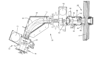
Turning now to the drawings, Fig. 1 depicts an ion
implanter, shown generally at 10, which includes an ion
source 12 for emitting ions that form an ion beam 14 that
traverses a beam path to an implantation station 16.
Control electronics (not shown) monitor and control the ion
dosage received by the wafers within a process chamber 17 at
the implantation station 16.
The ion source 12 includes a plasma chamber 18 into
lo which source materials are injected for ionization. The
source materials may include an ionizable gas or vaporized
source material. Energy is applied to the source materials
to generate positively charged ions in the plasma chamber
18. The positively charged ions exit the plasma chamber
interior through an elliptical arc slit in a cover plate 20
overlying an open side of the plasma chamber 18.
Ions in the plasma chamber 18 are extracted through the
arc slit in the plasma chamber cover plate 20 and
accelerated toward a mass analyzing magnet 22 by a set of
electrodes adjacent the plasma chamber cover plate 20. The
mass analyzing magnet 22 is supported within a magnet
housing 32. The strength of the magnetic field is
controlled by the ion implanter control electronics. The
magnet's field is controlled by adjusting a current through
the magnet's field windings. The mass analyzing magnet 22
causes the ions traveling along the ion beam 14 to move in a
curved trajectory so that only ions having an appropriate
atomic mass reach the ion implantation station 16.
Before reaching the implantation chamber the ion beam
14 is further shaped, evaluated and accelerated due to the
potential drop from the high voltage of the mass analyzing
magnet housing 32 to the grounded implantation chamber. The
beamline travel path from the source to the chamber 17 is
maintained at a reduced pressure by vacuum pumps P1, P2
spaced along the beam line.
2193709
Downstream from the magnet 22 the ion implanter
includes a quadruple assembly 40, a pivoting Faraday cup 42
and an ion beam neutralizer 44. The quadrupole assembly 40
includes set of magnets oriented around the ion beam 14
which are selectively energized by the control electronics
(not shown) to adjust the height of the ion beam 14. The
quadrupole assembly 40 is supported within an implanter
housing 50. Coupled to an end of the quadrupole assembly 40
facing the magnet 22 is an ion beam shield plate 52. The
plate 52 functions in conjunction with the mass analyzing
magnet 22 to eliminate undesirable ion species from the ion
beam 14.
The Faraday flag 42 is located between the quadrupole
assembly 40 and the ion beam neutralization apparatus 44.
The Faraday flag is pivotably coupled to the housing 50 so
that it can be pivoted into position to intersect the ion
beam 14 to measure beam characteristics and, when the
measurements are satisfactory, swung out of the beam line so
it does not interfere with wafer implantation at the
implantation chamber 17.
A prior art ion beam neutralizer 44, commonly referred
to as an electron shower, is disclosed in U.S. Patent No.
5,164,599 to Benveniste, which issued November 17, 1992, and
is assigned to the assignee of the present invention.
Ions extracted from the plasma chamber 18 are
positively charged. If the positive charge on the ions is
not neutralized prior to implantation of the wafers, the
doped wafers will exhibit a net positive charge. As
described above and in the '599 patent to Benveniste, such a
net positive charge on a wafer has undesirable
characteristics.
A prior art ion beam neutralizer is disclosed in
copending Canadian Patent Application Number 2,181,076
2193709
filed July 11, 1996 to Blake.
Directly upstream of the neutralizer 44 is a magnetic
repeller 110. Components of the repeller 110 are
schematically shown in Figure 3. The repeller 110 includes
permanent magnets M1, M2 for inhibiting backstreaming of
electrons from the neutralizer. The magnets M1, M2 replace
the biased ring aperture R discussed above in relation to
Figure 2.
The neutralizer 44 disclosed in Figure 1 bounds an open
ended, cylindrical interior region large enough to allow the
beam to pass unimpeded while neutralizing electrons are
injected into the ion beam. The neutralizer 44 and the
repeller 110 are shown in Figure 1 as being formed as an
integral unit and are supported by a common base 52 attached
to the housing 50.
Rotatably supported within the implantation chamber 17
is a disk shaped wafer support (not shown). Wafers treated
by the beam are positioned near a peripheral edge of the
wafer support and the support is rotated by a motor (not
shown) at a rate of bout 1200 RPM. The ion beam 14 impinges
on the wafers and treats the wafers as they rotate in a
circular path. Multiple wafers are supported around the
edge of the wafer support and are loaded and unloaded
2s through a load lock to allow the beam line to remain
evacuated during loading and unloading.
The implantation station 16 is pivotable with respect
to the housing 50 and is connected thereto by a flexible
bellows 92. The ability to pivot the implantation station
16 permits adjustments to the angle of incidence of the ion
beam 14 as the beam impacts wafers within the implantation
chamber.
Maqnetic repeller 110
Figure 3 schematically illustrates operation of the
magnetic repeller 110. The two permanent magnets M1, M2 are
2193709
spaced on opposite sides of the ion beam 14. A north pole
face 122 of the first magnet M1 faces the ion beam 14 on one
side of the beam and a south pole face 124 of the second
magnet M2 faces the ion beam on an opposite side of the ion
beam. Field lines between the two magnets are illustrated
in the Figure 3 depiction. Electrons moving through the ion
beam from locations either upstream or downstream from the
magnetic repeller 110 experience a force when they move into
the magnetic field between the magnets M1, M2.
lo An important advantage of the invention is illustrated
by the Figure 3 depiction. Electrons already located
between the two magnets M1, M2 are not swept away from their
positions within the ion beam. The negatively charged
electrons within the magnetic field do not experience a
force unless they are moving. If they do experience a force
due to random movement within the ion beam they tend to move
along spiraling paths 130 back and forth across the ion beam
14. These electrons continue to help neutralize the beam
rather than being swept from the beam due to the presence of
electric fields set up by a prior art suppression electrode
or ring R (Figure 2).
Figures 4 and 5 illustrate an alternate embodiment of a
magnetic repeller having field defining structure that
bounds the two elongated bar magnets N1, M2. Elongated bars
142, 144 constructed from a ferromagnetic material cause the
magnetic field lines to be concentrated on the side of the
ion beam 14. The presence of the magnetic bars allows field
lines to cross from the south to the north pole but
restricts the region in which highly concentrated field
lines occur.
Figures 7-9 illustrate an alternate and presently
preferred structure for mounting a repeller 140 that is
separate from the neutralizer 44. A metal base 150
supported by the implanter housing 50 includes an inwardly
facing surface 152 that abuts the housing 50 around an
access opening in the housing 50.
2I93709
The base 150 is secured to the implanter housing 50 by
means of threaded connectors 154 that engage appropriately
located openings in the housing 50. An elastomeric gasket
160 fits within a groove 162 (Figure 8) in the base and
seals the implanter interior to allow the implanter 10 to be
pumped down to sub-atmospheric pressures. To remove the
repeller 140 the connectors 154 are loosened and the base
lifted away from the implanter housing 50. A lead shield
162 overlies the base 150 and shields the region of the
repeller 140 from ionizing radiations in the region of the
implanter.
A bracket 170 attached to the base 150 is connected by
a support frame 172. The support frame 172 has four sides
and as seen in Figure 9 is generally rectangular in plan.
Four connected side walls 173-176 surround the ion beam 14
and directly support the repeller 140.
The repeller 140 includes two magnets M1, M2 and two
graphite shields 180, 182 supported by the frame 172. The
graphite shields 180, 182 prevent the ion beam 14 from
directly contacting the magnets M1, M2. The magnets M1, M2
set up a generally uniform dipole field in a region between
the magnets. The magnetic lines of force set up by this
field are illustrated in the Figure 9 depiction of the
repeller 140.
Each magnet such as the magnet M1 in Figure 7 is made
up of two abutting bar magnets 190, 192 which can be seen in
the phantom view of Figure 7. The magnets 190, 192 are
aligned end to end with the south pole of one magnet
abutting the north pole of the adjacent magnet. The
repeller preferably uses four identical magnets constructed
from samarium cobalt and having a surface field strength of
at least 2S00 gauss. In a typical implanter the ion beam is
shaped to be about 0.7 inches wide at the location the beam
passes through the neutralizer 44. To allow unimpeded
passage of the ion beam through the magnetic repeller 140
2I9370~
the two magnets M1, M2 are spaced apart by about 2.8 inches.
Figure 6 is a graph of ion beam transmission as a
percentage of the beam which leaves the mass analysis magnet
22. This efficiency is plotted as a function of beam energy
in kev. Two different sets of data are depicted. The data
points for a prior art ion implanter that utilizes a
suppression electrode or ring R biased at a negative
potential are plotted with `x's on the graph. The data
points on the graph designated with `o's are for an ion
implanter having a magnetic repeller such as the repeller
140 shown in Figures 7-9. The transmission efficiency is
seen to have improved from approximately 60% for the prior
art implanter to an efficiency of greater than 80% for the
implanter using a magnetic repeller 140.
While the present invention has been described in some
degree of particularity, it is to be understood that those
of ordinary skill in the art may make certain additions or
modifications to, or deletions from, the described present
embodiment of the invention without departing from the
spirit or scope of the invention, as set forth in the
appended claims.