Note: Descriptions are shown in the official language in which they were submitted.
21 ~4022
CA9-96-018
WIRELESS COMMUNICATIONS SYSTEMS WITH
SELF THRESHOLD SETTING
Field of the Invention
The present invention relates to col...l.unications systems and more particularly to a voltage
col,lpal~lor circuit which makes use of both delayed and real time inputs to adjust its
threshold values to respond to various inputs in order to reduce the effects of fluctuating
5 signal strength or signals of a wide dynamic range for the duration of the co"""lll~ications.
Background of the Invention
Wireless or light co"""~ ication systems, particularly infrared col,ll--unications systems have
a number of problems to deal with in effecting successful co"""ll"ications. One of the
10 char~ctP.ri~tics of wireless con~ ul~ications, in particularly infrared co~ -ications, is that
the signal being received at a receiver may vary by many orders of magnitude because of
differences in transmitter power, direction, atmospheric effects, distance, absorption, and
other effects that interfere with signal tran~mi~sion. In addition there is significant noise
from other sources of heat and light that i~ .rele with infrared co-~ ications, and for this
15 purpose, special ci~.;uil y has been used to enhance the reception of the true signal being
transmitted. The signal being tran~mitte~ is typically in the form of digital pulses, which
would, under ideal conditions, easily be perceived by the receiver. Because of the
inl~Çclellce that may be present, as mentioned, conventional circuits use a comparator which
col..pales the received signal to a threshold value.
21 q4022
CA9-96-0 1 8
In the infrared co~ lul,ication, a photodetector is used to detect infrared signals received and
produces electric pulses in response to the infrared signals. The electric pulses produced
by the photodetector are typically amplified and the resultant amplified digital pulse stream
is compared to an int~m~l decision threshold voltage by means of a voltage comparator and
5 based on the comparison made, the comparator will produced an output pulse if the voltage
threshold is exceeded.
In other fields of co-~ ul~ications a fixed threshold may be satisfactory; however, in the
wireless or infrared col~ u~ications fields, a fixed threshold can cause numerous problems
10 due to the wide variations in the signal. These variations will cause dead zones, fading, and
pulse widths that are too wide or too narrow to be handled by the receiving circuitry. When
the signal strength is too high, because of a nearby tr~n~mit~er, for instance, the pulse widths
being received may be too large for the receiver circuilly to handle; correspondently when
the transmitter is either too weak because of positioning or distance then the pulse width
l 5 determined by the comparator circuit would be too narrow for reliable processing.
U.S. Patent 4,459,311 issued October 17, 1995, assigned to Hewlett-Packard Company, Palo
Alto, California, is directed to a fibre optic system of a fixed length that includes both a light
source for producing optical signals, and optical fibre coupled to the light source to transmit
20 the optical signals. A photodetector is coupled to the optical fibre to detect those optical
signals and convert them to electrical signals. A delay line is coupled to the photodetector
to delay the electrical signals from the photodetector for a period sufficient for the decision
threshold circuit, which includes a peak detector, to detect the peak voltage of the first pulse
received in a coll-ll,ullication tr~n~mi~sion. The threshold voltage is set to half of the peak
25 voltage ofthe first digital pulse received. This threshold setting is m~int~ined for the rest of
21 q4022
CA9-96-0 1 8
the transmission. In addition, as the peak voltage is used a problem is encountered which
requires compensation for a cumn~ ve DC offset voltage.
As the reference is directed to a fibre optics system in which the system itself is a fixed
5 configuration, ie: the transmitter, receiver, and optical fibre line are fixed to each other; the
variations in signals expected would not result in a large change over short periods of time,
eg. during the currency of a transaction. The variations indicated by the reference vary by
no more than 20 dB and this variation is not generally time related. It is apparently related
to the length of fibre chosen for each system, and the strength of the transmitter. So a given
10 receiver having an effective range of signal strength acceptance can be used in different fixed
installations. The system disclosed apparently cannot compensate for variation in signals
during a communication period as it sets its threshold only at the beginning of a
col,u"unication period.
15 In the optical fibre collllllullication system, once established the signal amplitude is constant
and typically only one co~ l,unication protocol is used such as SONET (SDH). However,
in infrared co"ll"ullication, the co~"~"ullication distance may vary over time during the
tr~n~mi~sion. For instance in a mobile infrared telephone the users may be moving with
respect to each other. The signal amplitude changes within a very large range over time and
20 the receiver expected to operate in this environment must also handle a large number of
di~el~ comn-unication protocols. This in turn poses a problem which the reference does
not appear to be able to handle. In the reference the question left unsolved is how long
should the peak value detected for the first pulse be kept, and when should it be updated.
As we have discussed, this is not a critical problem in a fibre optic co"ll"unication system
25 where one protocol is being used. However, in the infrared field and when different
21 94022
CA9-96-01 8
communication protocols are being used, the pulse duration and pulse separation can be
widely di~elenl for the IrDA 2.4 Kbs protocol the pulse duration varies between 1.41 ,us to
85.55 ,us. For the IrDA 1.152 Mb/s protocol standard the pulse duration may vary between
147.6 to 260.4 ns. This poses a serious problem for prior art systems such as the reference.
5 We have found by experimentation, that peak detection system does not work properly in
infrared communications.
It is therefore desirable to use the instant signal as a basis for adjusting the threshold.
Another basic problem for wireless communications is due to the base line shift caused by
lO AC coupling which is used to reduce environmental noise. Peak detection circuits cannot
compensate for this, whereas, it is desirable to handle this situation as well in order to
achieve successful communications flexibility.
Summ~ry of the Invention
15 The present invention overcomes the difficulties posed by the prior art. In its preferred
embodiment the invention is capable of accepting a wide input dynamic range of signals up
to five orders of magnitude (50 dB) while overcoming the difficulties presented by many
colmnu fications protocols such as the pulse position protocol system which is widely used
in infrared co.~ lunications.
Conventional fixed threshold settings cause the output pulse width of an amplified
photodetector input to strongly depend on the input signal amplitude so that the signal may
exceed the threshold required for effective collllllullication but the co-l~llunication will still
fail because the output pulse is either too wide or too narrow with respect to the requirements
25 of the colll-llu lication protocol being used. If a fixed threshold is used a strong signal may
21 94022
CA9-96-0 1 8
cause a very wide output pulse and may result in two pulses being merged. Conversely, if
a small signal is received the resultant pulse may be too narrow.
The invention provides a co~ ication system that can be useful in the infrared spectrum
5 which includes a photodetector for detecting infrared signals from an infrared source and
converting the infrared signals to electrical signals; a first delay device having an input
coupled to the photodetector for delaying the signal from the photodetector for a period of
time related to the rise time of an expected electrical signal from the photodetector; a voltage
divider having a input coupled to the photodetector for reducing the amplitude of the signal
10 from the photodetector; a second delay device having an input coupled to the output of the
voltage divider for delaying the reduced signal from the photodetector for a predelelll~ ed
period of time related to the fall time of an expected electrical signal from the photodetector;
a first voltage colll~al~lc,r coupled to an output of the first delay device and to the output of
the voltage divider for comparing the signal received therefiolll and adapted to generate the
15 front edge of a voltage output in response to the detection of the front edge of a pulse from
said photodetector; a second voltage comparator coupled to the photodetector and to an
output of the second delay device for generating the back edge of a voltage output in
response to the detection of the back edge of a pulse from the photodetector.
20 In addition, the invention advantageously provides for the outputs of the first and second
comparators be coupled to the inputs of an AND gate to produce an output pulse from the
AND gate when the outputs of the two voltage colllpal~tors are active.
Brief Description of the Drawings
25 These and other features of the present invention will be better understood with reference to
21 94022
CA9-96-018
the following detailed description when considered in connection with the accompanying
drawings in which:
Figure 1 is a generalized block diagram representation of an infrared communication circuit
5 having a fixed threshold in accordance with the prior art;
Figure 2 is a block representation showing a specific implementation of the present
invention;
Figure 3 is a block representation showing a second specific implementation of the present
10 invention;
Figure 4 depicts input and output waveforms for the circuit of Figure l;
Figure 5 depicts input and output from the implementation of Figure 2;
Figure 6 depicts input and output waveforms for the Figure 3 implementation.
15 Detailed Description of the Drawings
Referring to Figure 1, an infrared co~ ication system having a fixed voltage threshold
input Vth is illustrated. The system includes a photodetector 1 coupled to an amplifier 2 the
output of which, VO is fed to the input 4 of voltage comparator 3. In addition, co~ or
3 is provided with a fixed threshold voltage at input 5.
When voltage comparator 3 is presented with an electrical pulse on input 4 from the
amplified output of the photodetector an output VCO will be produced at the output at terminal
6 in accordance with detected pulses received that exceed the fixed threshold voltage.
25 There has been found that such a circuit is inc~p~ble of handling a wide input dynamic range
21 q402~
CA9-96-0 1 8
of up to five orders in magnitude (50 dB) may occur in infrared co~ ications. Inaddition, the protocol of the pulse position modulation that is widely used in infrared
communications requires a circuit output pulse width to fall within specific limitations as
indicated previously. The conventional fixed threshold circuit of Figure 1 will have an
5 output voltage pulse width (from voltage comparator 3) strongly dependent on the input
signal amplitude. So that if the signal amplitude exceeds the threshold by a large amount,
then co~ cations will fail because the output pulse will be too wide to be acceptable to
the infrared collllllul~ication protocol. If the input pulse is too weak to exceed the threshold
by a significant amount, the coll~ ication will fail because the output pulse will be too
10 narrow to fall within the requirements of the collllllullication protocol.
An analysis of the pulse width dependency of the circuit of Figure 1 is discussed below:
The output pulse width of VCO is expressed in the following formula when the fixed threshold
15 V,h is set to half minimum input pulse amplitude multiplied by the system small signal gain
(ie. no saturation effects).
PwO = PWi + ~ Ln {(2Vin/Vmjn-l) * [l-exp(-PWj/~)]} (1)
Where PWO: output pulse width of VCO
PWj input pulse width
Vjn: input pulse amplitude
T: system time constant and ~ = (2~BW)-'
BW: system bandwidth
Ln: natural logarithm
- 21 94022
CA9-96-0 1 8
exp: natural exponential
A detailed calculation of this is shown in Appendix A.
5 As can be seen, the output pulse width depends on the input pulse amplitude. It should be
pointed out especially that when t = T, the input pulse period, then at the moment the next
pulse starts, there is still a residual voltage, Vre present from the previous pulse where
Vre= [1-exp(-PWj/ I)]* exp[-(T - PWj)/ T] * K * Vjn
where K = system small signal gain
T = input pulse period
When the input pulse amplitude is large enough so that Vre reaches the level of V~, it results
in the merger of the two pulses into one, and the collllllunication will definitely fail. This
limits the system input dynamic range to
15 Vre= Vth= KVmin /2 or
Vm~Vmjn = exp[-(T-PWj) /T)]/~2*[1-exp(-PWj / T )]}
where Vm"~ = maximum input pulse amplitude
Using 4 Mb/s IrDA protocol and a fixed threshold the dynamic range will be limited to about
20 2 orders (ie. 20 dB) of magnitude.
We have determined that one solution to the problem is to use a comparator in which the
comparator threshold is not fixed but is derived from the photodetector amplifier output
itself. In this way, when the input pulse received is large the threshold voltage becomes
25 high; when the input pulse received is small, the threshold voltage is reduced. In this manner
21 94022
CA9-96-0 1 8
we have delel-lJilled that the output pulse width will kept constant, irrespective of the
magnitude of the input pulse amplitude.
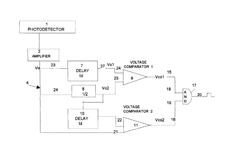
One embodiment in accordance with the invention with self threshold setting is shown in
5 Figure 2.
It can be seen that the communication circuit of the embodiment of the invention depicted,
comprises a photodetector 1 capable of detecting infrared signals from an infrared transmitter
source and converting the infrared signals to electrical signals.
In this embodiment the output of the photodetector is amplified by amplifier 2 to produce a
photodetector output voltage VO on line 4.
A first delay device 7 has an input 23 coupled to the output of the photodetector on line 4 for
15 delaying the signal from the photodetector for a predete~ ined period of time td (which is
related to the rise time tr of the expected electrical signal from the photodetector.) We have
found that delay time td should be close to the rise time tr~ for instance if the rise time is 35
ms in the case of the 4 Mb/s IrDA protocol a time delay td of 20 to 50 ns will be effective.
less delay can be used if signal noise is small and the offset voltages of the colllpa~ators is
20 small.
Voltage divider 8 has an input 24 which is coupled to the photodetector output for dividing
the amplitude of the signal from the photodetector by a predetermined amount. In the case
of Figure 2, it is dividing the signal by half.
- 21 ~4022
CA9-96-0 1 8
A second delay device 10 has an input 26 coupled to the output 25 of voltage divider 8 for
delaying the signal from the photodetector 1 for the period of time td.
The first voltage comparator 9 is coupled to output 27 of the first delay device 7 and to the
5 output 25 of the voltage divider 8 for coll~palillg the signals received from them at input
t~nnin~l~ 24 and 23 of the voltage comparator 9 to generate the front edge of a voltage output
VcOl on upper terminal 15 the response to detection of the front edge of a pulse from the
photodetector 1. The second voltage comparator 11 is coupled by input terminal 21 to the
photodetector 1 and by terminal 22 to the output 28 of delay device 10 for generating the
10 back edge of a voltage output Vc02 in response to the detection of the back edge of a pulse
from the photodetector 1.
The input t~nnin~l 18 and 19 AND gate 17 are coupled to the outputs 15 and 16 respectively
of voltage comparators 9 and 11 and produces an output pulse on its output gate 20 in
15 response to its outputs of the voltage colllpal~lol ~ 9 and 11 producing a suitably shaped pulse
when the outputs 15 and 16 of colll~al~lol~ 9 and 11 respectively are active. This pulse will
correspond in width with the infrared pulse received by photodetector 1 and will be relatively
independent of the input amplitude received by the photodetector.
20 The output of the AND gate 17 will comprise a series of pulses in accordance with the
infrared pulses detected by photodetector 1 and can be further processed by circuitry and or
software which will not be described as it is not the subject of this invention for the handling
of received information thereby.
25 In the embodiment of Figure 2, the amplifier output signal VO is delayed in time and/or
21 q4022
CA9-96-0 1 8
divided by 2 in amplitude to generate VOI~ but Vo2 and Vo3.
VOI has the same amplitude as VO7 but is delayed to tdin time.
Vo2 has the half amplitude of VO~ but is not delayed.
Vo3 has the half amplitude of VO7 and is delayed by td in time.
5 VOI and Vo2 are connected to the inputs of voltage comparator 9 to generate the front edge
of the circuit output pulse.
VO and Vo3 are connected to the inputs of voltage comparator 11 to generate the back edge
of the circuit output pulse.
Vo2 and Vo3 are essentially used as the thresholds of the comparators. Their values are not
10 preset to a fixed value, but depend on the signal amplitude itself. This is called self threshold
setting.
The output pulse width is shown below:
PWO= I* In {[2 * exp (PWj/ ~ ) -2 + exp (td 1~)]1[2* exp (td / ~) - 1]} (2)
15 where td: delay time for Vo2 and Vo3 and other variables are the same as in equation ( 1) above.
Equation (2) shows the circuit output pulse width is independent of the input amplitude, and
accordingly all problems caused by dependence of output pulse width on input amplitude
have been solved.
20 Appendix B shows the detailed derivation.
It has been determined that the delay time that will produce s~ f~ctory results in this
invention as depicted in the specific embodiment, depends on the bandwidth of the
co.~ unication system designed. The delay time td should be approximately the same as the
25 rise time of a pulse tr. It is well known in the art that the rise time of a pulse is defined as the
~1 q4022
CA9-96-01 8
time interval that it takes for the pulse to rise from 10% of the pulse amplitude to 90% of the
final pulse amplitude. It is also well known that the co~ ication system bandwidth
determines pulse rise time and that pulse rise time can be calculated according to the formula
[tr = 350 / bandwidth] in which the rise time will be determined in nanoseconds and
bandwidth is represented in Megahertz.
In the current IR technology, bandwidth has been kept to 10 Megahertz or less so the rise
time expected in such a system for a pulse is 35 nanoseconds or longer.
It has been found that the amplitude ratio chosen in this embodiment for the voltage divider,
namely 0.5 is a satisfactory value as it tends to keep the output pulse width approximately
the same as the pulse width of the input provided to it.
In the high speed infrared field for which this device is adapted, the rise and fall times of
pulses being transmitted are very fast so that the pulse shape approaches that of bell with
curved rise and falling edges. The comparator circuit generates in response to this a shaped
pulse that is suitable for use by digital processing and decoding circuits following or attached
to this device.
Referring to Figure 3, another embodiment of the invention is shown. We have found that
the output pulse width of this circuit will be kept very close to the width of the input from
the photodetector. This is illustrated in Figure 6.
In this circuit the second comparator 11 receives as its inputs the outputs of the first delay
device 7 and the second delay device 10. Delay device 10 is adapted in this embodiment to
21 94022
CA9-96-018
delay the signal by approximately 2 td (ie. Twice as much as imposed by the first delay
circuit).
The delay devices depicted in the drawings and text have not been discussed in detail as
5 those f~rnili~qr with the art would be well able to use suitable devices in order to achieve the
objectives of the invention without difficulty. Suitable delay devices would include RC
filters and analog delay lines or such other devices as may be known in the art.
13
21 q4022
CA9-96-018
APPENDIX A
Calculation of Output Pulse Width (Fixed Threshold)
This Appendix, taken together with Figure 4, illustrates the behavior of the circuit of Figure
1.
[I-exp (- t)] K Vin o~t~PWi
Vo(f)=~ [1-exp (_PWi)] K Vin exp (_t PWi) PWi~t~T
[I-exp (_PWi)] K Vin exp(-T PWi)] + [1-exp (_t T)] K Vin T~t~T+PV~
Where
Vo(t) = amplifier output
exp = natural exponential function
system time constraint, ~ = (2~BW)-
BW = system bandwidth
K = system small signal gain
Vin = input pulse amplitude
PWi = input pulse width
T = input pulse period
Usually the threshold is preset to l/2 K Vmin, that is:
Vth = 1/2 K Vmin
Where Vth = fixed threshold value
K = system small signal gain
Vmin = minimllm input pulse amplitude
14
2i 94022
CA9-96-0 1 8
Calculation of t" the cross point of the output pulse front edge and the threshold:
[1 -exp (- 1 )] K Vin = Vth = 1/2 K Vmin
t~ In ~ 2Vin- Vmin~
2Vin
Calculation of t2, the cross point of the output pulse back edge and the threshold:
[1-exp (_PWi)] K Vin exp ( f2 PWi~= Vfh = 1/2 K Vmin
f2 = ~ ln Vmin +PWi
2[1 -exp(- PWi)]Vin
The circuit output pulse width:
PWo = t2-fl = PWi+l In ~ V i -1) [1 -exp(- PWi)]
21 94022
CA9-96-01 8
APPENDIX B
Calculation of Output Pulse Width (Circuit of Figure 2~
This Appendix, together with the circuit of Figure 5, illustrates the behavior of the circuit of Figure
2.
The math expressions of Vo, Vo" Vo2 and Vo3 are shown below:
[1-exp (- ~)] K Vin o~t~PWi
[I-exp (_PWi)] K Vin exp (_t PWi) PWi~t~T
o ~td
V () [I-exp (-~ ~d)] K Vin ~d~tcPWi+~d (2)
[l-exp (_PWi)] K Vin exp ( f PWi ~d) Pwi+~d~T+~d
/2 [1-exp (- ~)] K Vin o~t~PWi
1/2 [l-exp (_PWi)] K Vin exp (_~ PWi) PWi~t~T
16
2 ! 94022
CA9-96-01 8
' o o~t~td
V () 1/2 [1-exp (_t td)] K Vin td~t~P Wi+td
l/2 [l-exp (_PWi)] K Vin exp (_t-P Wl-td) P Wi+td~t~ T+td
(2) and (3) determine the cross-point of tl, the output pulse front edge:
K Vin [1-exp(- I d)]=l/2 K Vin [1-exp( 1)]
t~ = ~ ln [2 exp ( d~ _ 1]
(1) and (4) determine the cross-point oft2, the output pulse back edge:
V [1 (_~Wi)] exp (_t2-1' Wi) = l/2 K Vin [1-exp( - )]
t2 = ~ ln {2 [ exp (_ P Wi) _ 1] + exp (td)}
The circuit output pulse width PWo is:
2exp(PWi) - 2 + exp(td)
P Wo = t2-t~ = ~ In~
2exp( td) -1
2 1 94022
CA9-96-01 8
While the cilcuilly of the invention has been described mostly in the context of infrared
communications, it can be appreciated that the invention can be applied to coll"~ullication
systems using other wavelengths of light.
While the present invention has been described with reference to a few specific
embodiments, the description is illustrative of the invention and is not to be construed as
limiting the invention. Various modifications to the invention may be made by those skilled
in the art without departing from the true spirit and scope of the invention as defined by the
appended claims.
18