Note: Descriptions are shown in the official language in which they were submitted.
W0 96104650 2 1 9 4 2 2 7 PCT~Us9sl07096
DUAL LAYER OPTICAL MEDIUM HAVlNG
PART~Al .1 .Y RE~ECl~G T~l EILM LAYER
Field of the Invention
The present invention relates generally to the field of optical media, and
more specifically to the area of optical media which employ two or more
'- storage layers.
Back~round of the Invention
There is a seemingly never-ending demand in the field of data storage for
media having increased storage capacity and p r.... ---, e In the field of pre-
recorded optical &scs, such as compact discs and video discs, increased storage
15 capacity is usuaUy achieved by increasing the storage density per unit area of the
disc. However, the maximum data storage density achievable in an optical
recording system is limited by the smallest feature that the optical system can
resolve. For .,~,.... ' far-field imaging systems, the smallest resolvable feature
size is limited by difflaction effects to alJp~ the ~ . ' , ' of the available
light source, usually a solid state laser diode. Thus, one method of increasing disc
storage capacity is to decrease the wavelength of the laser diode. However, while
the ~YD~.~ ,,' available from laser &odes have been steadily decreasing, the
decreases have not been dramatic due to limitations in solid state technology and
materials.
A number of other techniques for increasing storage capacity of optical
recordmg systems have been proposed. These include: (1) higher efflciency data
coding schemes, e.g., I ' ..;J~I. ' ' , (2) optical and/or magnetic super-
resolution; (3) zoned recording at constant angular velocity; (4) advanced data
channel detection methods, such as partial I~D~OOnS;~/III~IIIUIII likelihood detection,
30 and (5) recording on both the grooves and land areas of the disc.
While the preceding methods for increasing storage capacity all rely upon
increasing the storage density per unit area of the disc, an alternative method for
w0 96io46s0 2 1 9 4 2 2 7 r~l,., . . L
increasing the capacity of an optical disc is to employ additional storage layers on
the disc which can be L 1~ . L .~lly recorded or reproduced. Thus, the approach in
this case is to increase the add.~le area of the disc. This approach is attractive
because it has the potential to ' ~l~ increase media storage capacity with
only a modest increase in media and recording system complexity.
Tf multiple storage layers, e.g., 2, are to be reproduced by optical beam(s)
provided on one side of the disc, then one of the storage layers of the disc must be
reflective enough so that it may be reproduced by the optical beam(s), but
transparent enough so that the beam(s) may penetrate the first storage layer andpass on to a second storage layer. However, such a disc has proved to be difficult
to construct, especially, where only a single laser is employed.
.~nmrr ~y of th~ InvPnti~m
Accordingly, the present invention provides an optical disc having a partially
rerdecting layer and a transparent spacer layer that allows a single .~q,.-' _
optical beam to focus on either of two different plames within the disc. The disc
includes a tr~msparent substrate having a pattem of pits in one of its sides. A
partially reflective layer adjacent the pit pattem has an index of refraction having a
real component (n) between 2.6 and 3.2 and an imaginary component (K) less than
0.4, measured at any wavelength within the range of from 500 to 850 nm. A
transparent polymer spacer layer is provided over the partially reflective layer, and a
highly reflective layer is provided over the spacer layer.
In one '-" of the present invention, the substrate comprises
pcl~l and the spacer layer comprises a PI~ JVI~ . A second pattem of
pits may be provided in the side of the spacer layer adjacent the highly reflective
layer. The internal surface reflectivity of the partially reflective layer preferably
varies by less than +0.03 over variations in thickness in the partially reflective layer
of _10~/~. The spacer layer has a thickness of from about 5 to 100 ~Lm.
In another; b~ " of the present invention, the partially reflective layer
includes silicon carbide. One preferred ratio of the silicon to the carbon in the
partially reflective layer is 1:1.3. In yet another ~i I ' t, the partially reflective
WO 96/04650 2 l 9 4 2 2 7 r~
layer includes silicon carbide containing from about 5 to 15 atomic % oxygen. The
partially reflective layer is preferably 30 to 80 nm thick.
The present invention also includes optical storage systems which include
the media described above. The systems further include a focused laser beam
positioned to enter the medium through the substrate, means for adjusting the focal
position of the laser beam on either the partiaUy reflective or highly reflective layer,
and a l' ' positioned to detect the reflected laser beam exiting the
medium.
As used herein, the terms "silicon carbide" or "SiC" mean mixtures of silicon
and carbon ranging in cu ~ from 30-50 atomic % silicon, 35-60 atomic %
carbon, and 0-20 atomic % oxygen, as measured by x-ray ,uLùLù~le.,l~un
~ ,L~u~,u~)y~ and having silicon-carbon ' ranging from SiCog to
SiC~
Brief Descrigtion of the Drawing
FIGURE I shows an optical data storage system according to the present
invention.
FIGURE 2 is a computer-generated graph of internal interface reflectivity at
650 nm as a function of thickness for various materials.
FIGURE 3 is a computer-generated graph of internal surface reflectivity at
650 nm as a function of thickness for silicon carbide according to the present
invention.
FIGURE 4 is a computer-generated graph of apparent reflectivity at 780 nm
as a function of thickness for silicon carbide according to the present invention.
FIGURE 5 is a graph of the real component of the index of refraction (n) as
a function of wavelength for various materials according to the present invention.
FIGIJRE 6 is a graph of the imaginary component of the index of refraction
~K) as a function of wavelength for various materials according to the present
invention.
FIGURES 7A-7C show I ' u~ hs of various layers of the optical
recording medium ~,u~l ~Llu~,Lcd according to Example I .
-3-
wo 96/046s0 2 ~. 9 4 2 2 7 I~ 6
n ~ ~ Descriptiorl ~.
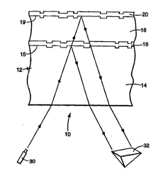
An optical data storage system 10 according to the present invention is
shown in FIGURE 1. Optical storage medium 12 comprises a transparent substrate
14, a partially reflective thin film layer 16 on a first data pit pattern 15, a transparent
spacer layer 18, and a highly reflective thin film layer 20 on a second data pitpattern 19. An optical laser 30 en~its an optical beam toward medium 12, as shown
in FIGURE 1. Light from the optical beam which is reflected by either thin film
layer 16 or 20 is sensed by detector 32, which senses ' ' - in light intensity
0 based on the presence or absence of a pit in a particular spot on the thin film layers.
Although patterns 15 and 19 are referred to as "data pit pattems," pit
patterns 15 and 19 may be any pattern of pits or grooves that is capable of storing
'- , be it data, servo or tracking r ' , format r ~ ~ etc.
The capabilit,v for ' ~" ' 1~, reading either the first or second pit pattern
15 or 19 is based on the ~,u~u~ iv~l~ limited focal depth ~.Lvv~ , of typical
optical disc readout systems. The lenses employed in typical optical
c~,uld~ L.~_.v to form a diflfraction limited laser radiation spot on the media
storage layer have moderately large (0.4 to 0.6) numerical apertures to improve
resolution and increase storage density. Such lenses exhibit focal depths (i.e., the
range of focus variation over which the focused spot size remains ~
diflraction limited) of about 2 llm; for large focus variations the size of the
illuminated spot grows rapidly. C~ , if partially reflective thin film layer
16 exhibits adequate and the distance separating the two data pit
pattems 15 and 19 is large relative to the optical system focal depth, it is possible to
2s focus the laser 30 on either data pi~ pattern with acceptably low "cross-talk" from
the other data pit pattern. Thus, although the light from laser 30 will be reflected
back toward detector 32 by both layers 16 and 20, only the layer upon which lhe
laser is focused will strongly modulate the reflected light intensity, thereby enabling
data readout.
30The data pit patterns 15 and 19 on medium 10 can be reproduced most
easily by first focusing on one of the reflective layers 16 or 20, and then
w096l04650 ~ 1 9 4 2 ~7 Y~
IqJI~ ~U ' ,, the data on that entire layer before switching focal position to focus on
the other reflective layer. In the alternative, it may be desirable to switch focus
position one or more times before completely ltlJluJuv;llg the data contained m one
of data pit patterns 15 and 19. In either case, use of two data pit patterns separated
5 by transparent layer 18 effectively doubles the data storage capacity of optical
recording medium 10.
T . , substrate 14 may be a polymeric materiai suitable for opticai
disc substrates which supports moldmg of data pit pattern 15 with sufficient fidelity,
such as pol~ or amorphous polyolefin. Al ~ it is possible to use
o a flat substrate of, for example, glass or pGl~l...,Ll.J' ' ~iale~ and form data pit
pattern 15 by means of pl-V~U~/GI,r..l~l replication, as will be described for the
formation of data pit pattern 19.
T ,, spacer layer 18 may be a polymer, such as a pl,~,l.. ,.l11.
polymer, which has a complex refractive index with a reai r r t, n, ranging
from about 1.45 to 1.6 and an imaginary , t, K, of less than 10~ and more
preferably less than 105. Transparent spacer iayer 18 should be thick enough to
ailow laser 30 to focus on either of data pit patterns 15 and 19 with a minimum of
cross-talk. This translates into a thicicness that is preferably within the range of
from about 5 to 100 llm, and more preferably from about 30 to 5ollm
Highiy reflective layer 20 may be a metailic layer which exhibits high
reflectivity at the laser vvv~L,..,~ used to reproduce the data. Currently available
laser diode sources radiate at ~ ' ranging from about 600 to 850 nm.
Aiuminum, gold, silver, copper and their alloys can exhibit suitably high reflectivity
in this ~vvv, ' . ' range. Highiy reflective layer 20 preferably has a reflectance of
at least 70~/0, and more preferably at least 80%
In order to minimize the complexity and cost of optical data storage system
10, it is desirable that the average readout signai levels from each of the data pit
patterns 15 and 19 be vlJyl~ 1~, equal. Thus, the apparent l~Li~,~,Liv;l;.,v from
layers 16 and 20, as seen by detector 32, should also be vp~ , equai
As used herein, the term "apparent ~ ,livity" refers to the fraction of
opticai power incident upon transparent substrate 14 which, when focused to a spot
wo961046s0 2 1 9 4 22 7 . ~IIU~ S _ v G
~n a flat region of either layer 16 or 20, could, in principle, be sensed by a
in an optical readout device. It is assumed that the readout device
comprises a laser, an a~ ulJl;vLcl~ designed opticai path, and a ~ t n~ . It is
further assumed that the optical eiement in the opticai path which is in closest5 proximity to transparent substrate 14 is a high (>0.4) numerical aperture objective
lens. As used herein, the terms "intemai surface lcn~,~,LiviLy" or "intemai interface
c,n~~ " refer to the fraction of opticai power incident upon an interface withinthe media structure (e.g., the interface betveen transparent substrate 14 and
partiaily reflecting layer 16 or the interface between spacer layer 18 and highiy
lo reflecting layer 20) which is reflected.
In order to estimate the necessary reflectivity from partially reflective layer
16, we assume that highiy reflective layer 20 consists of aluminum, which reflects
about 80 to 85% of the light incident on the intemai interface between spacer layer
18 and highiy reflective layer 20. It is further assumed that the refractive index reai
1S : . t, n, of spacer layer 18 is 1.5, that substrate 14 is pul~,al~ with a
refractive index real ç/~mnr~n~nt~ n, of 1.57, and that reflections at the air-substrate
interface do not contribute to the readout signal. If we further assume that partially
reflecting layer 16 is an ideal materiai which exhibits no absorption, it can be shown
that a reflectivity of about 0.35, as observed at the intemal interface between
20 substrate 14 and the partially reflecting layer will yield a balance in the apparent
~-,n~,~,LiviLi~,v from layers 16 and 20. While a partially reflecting iayer 16 which
exhibits no absorption is ideal, reai partiaily reflecting layer materials are iikely to
exhibit some absorption. If we choose a h~u~h~,ti~.ai partially reflective layer which
absorbs 25% of the iight it does not reflect and define this as an upper limit for
2s acceptable absorption, we find that an intemal surface reflectivity of about 0.25 is
required to baiance the reflectivity of layers 16 and 20. In this case, the apparent
~cll.,~L;viLi.,D from both layers is about 30% less than for the case of a partially
reflecting layer which exhibits no absorption. Thus, the preceding examples define
a range for the intemai surface reflectivity at the interface between the substrate 14
and layer 16 of from about 0.25 to 0.35 Taking into account the attenuation due to
~ W096104650 2 1 9 ~ ~7 PCTIUSgS/07096
reflections at the substrate-air interface, the above range CUIIG~)UIIdS to am apparent
~ reflectivity seen by an opticai readout device of about 0.24 to û.33.
Candidate materiais for partiaily reflecting layer 16 include metais,
~ ' and dielectrics. Metais, however, are generally strongly absorbing
and may be expected to cause excessive signai at~pn~ on Ful~h~ u~ the
reflectivity of metaiiic fiims typically is a very strong function of film thickness.
FIGURE 2 is a computer-generated graph based on optical modeling showing
intemai surface reflectivity for incident iight of ~va~ ll 650 nm as a fiunction of
thickness caiculated for films of gold (Au), aiuminum (Ai), and siiicon (Si) films
10 sall;i~ ~i between a 1.2 mm thick pOly~al~ substrate and a slab of n= 1.5,
I~ = û material, which a~ u~;lllatl~D the effect of transparent spacer layer 18.r - of FIGW~E 2 reveals that the reflectivity of an Ai or Au
partially reflecting layer chamges very rapidly with thickness, making control of film
thickness and unifomlity during lllal.ura~,tul~: very difficult. An amorphous layer of
15 the ! ' ~ S; exhibits behavior which is similar to that of Au over the
desired reflectivity range of û.24 to U.33; i.e., small changes in film thickness result
in substantiai changes in reflectivity. r...Lh~....ul~, films with l~iu~,~iviL.,i~ in the
desired 0.24 to U.33 range would be oniy about 4 nm thick for Ai and about 15-2ûrlm thick for Au and Si. Such relatively thin films may exhibit poor ~,.,~;.~ '
stabiiity.
In contrast to the behavior depicted in FIGURE 2, I have found that a
partiaily reflective film comprising amorphous siiicon carbide exhibits reflectivity vs.
tbickness behavior which is much more desirable. As shown in FIGURE 3, which is
a computer-generated graph based on opticai modeiing, the intemai surface
reflectivity at 650 mm lies within the desirable range of from about 0.24 to 0.33 for
amorphous siiicon carbide fihm thicknesses ranging from about 35 nm to 65 nm.
Smail changes in thickness within this range have a much less p~ u~luu.l~ d effect on
reflectivity than is observed for the materials depicted in FIGURE 2. C~r-~q~
*e r ' ~ / of a duai layer disc comprising a siiicon carbide partiaily
reflecting layer is greatly improved relative to that of a dual layer disc comprising
partiaily reflecting layers with ~,La~ a~ Lh~ such as those depicted rn FIGURE 2.
W096/04650 2 19 4 2 2 7 r_l,.S . .~ ~
The complex refractive index used to generate the graph shown in FIGURE
3 was determined for an amorphous silicon carbide film having a~.y~ , 42
atomic % silicon, 53 atomic % carbon, amd 5 atomic % oxygen, as measured by x-
ray, ' ' ua D~ LluDcu~Jy. The highly dcsirable behavior shown in FIGURE 3
5 results from the complex refractive index ~ ul~ L;u of amorphous silicon
carbide. The relatively low value of K (~0.19 at 650 nm) results in acceptably low
attenuation of the signal from second data pit pattern 20, and in . ' with
the relatively large value of n (~3.07at 650nm), yields a first maximum in
reflectivity as a function of thickness that lies within the desired range for the
lo FIGURE I media ..o..~.u, The small rate of change in reflectance versus
thickness on either side of the maximum yields the highly desired viLy of the
reflectance to variations in the thickness of partially reflecting layer 16.
As noted previously, in addition to having a partially reflective layer for
which reflectance changes only slowly with thickness variations, it is also desirable
15 that the apparent ~;n~LiviLi~D from layers 16 and 20 be ~ Jlwd~ LulJ equal, and it
is most desirable that both . ~ n. ~ occur over the same range of partiallyreflectmg layer i' ' Stated differently, it is most desirable to have a media
CUIIDLIU~LiUII for which the apparent ~r~ iviLkD from layers 16 and 20 are both
".~, equal and insensitive to layer 16 thickness variations. This situation is
20 depicted ' '1~ in a computer-generated graph based on optical modeling
shown in FIGURE 4 . Inspection of FIGllRE 4 reveals that the apparent
~t n~ ~Livi~ D from layers 16 and 20 differ from one another by less than about
_ 0.03 for partially reflecting layer thicknesses ranging from about 50 to about 80
nrn, i.e., a thickness variation from a nominal value of 65 nm of more than + 20%.
25 It can be shown that the absolute values of apparent reflectivity for both layers 16
and 20 depend upon both the real and imaginary r~ - ~~ of the partiaOy
reflecting layer complex reflractive index, and that the behavior shown in FIGURE 4
occurs for only a narrow range of complex refractive index values.
Using the previously described ~ . regarding the reflectsmce of the
30 highly reflective layer and the optical properties of the substrate 14 and
~LUL~ U /~ Iayer 18, it can be shown that a SiC partially reflective layer (similar
~ W0 96/046~0 2 1 9 4 2 ~ 7 P~ v. E
in . . to the film used in FIGURE 3) will exhibit behavior ' 'ly
identical to that depicted in FIGURE 4 when used at a ~4a~,L l.~,LIl of 780 nm, i.e.,
the ~a~lul~ Il used by currently available compact disc players. Amorphous
silicon carbide, thus, is close to an ideal material for use at this ~a~' ,,"
5 However, K varies as a function of ~av. ' ,," Use of amorphous silicon carbide- containing no more than 5 atomic % oxygen at ~a~ .S~ho in the 600-650 mm
range is some,vhat less ideal, however, as K has increased from about 0.12 at 780
nm to about 0.24 at 600 nm.
The a~ lu~ hlldt~ doubling of K results in less light i through
o partially reflecting layer 16, which reduces the apparent reflectivity from highly
re'decting layer 20. C.. l ~ly, the apparent ~cn~Livi~h,s from layers 16 and 20
will not be ' 'l~ equal over the desired range of partially refiecting layer
thi~ l-n.~cc~c Accordingly, it may be desirable to alter the physical properties of the
SiC to reduce K This may be , ' ' ' by the use of a dopant, such as silicon
dioxide.
The real and imaginary r ' of complex refractive index for three
different amorphous silicon carbide: . are shown in FIGURES 5 and 6
as a function of ~ ' These three specimens were prepared by UUv~UI ' ~,
from a silicon carbide target and a silicon dioxide target and changing the power
levels, resulting in three different amorph~us silicon carbide c ~ ~u~ -- - The first
CUIIIIJI "' contained about 42 atomic % silicon, 53 atomic % carbon, and 5
atomic % oxygen. The second and third amorphous silicon carbide l u~
contained about 8 and 12 atomic ~/0 oxygen, ,.,v~ ,Li~ . As shown in FIGURES 5
and 6, the complex refractive index of these materials varies with ~a~lul~5 h.
FIGURES 5 and 6 show that addition of oxygen to the amorphous SiC
reduces both n and K of the resulting mixture. As the reduction in n will decrease
the magnitude of the maximum refiectivity from the internal interface between
substrate 14 and layer 16 while the reduction in K manifests itself as increasedof light through layer 16, it is apparent that relatively small additions of
oxygen into SiC can be used to tune the optical properties of the resulting mixture
such that the highly desirable behavior ' "!~ depicted in FIGURE 4 can be
wo 96/0465~) 2 1 9 4 2 2 7 r~
obtained for ' '1~ any ~n~ ~ for which media operation is desired
within the 500 to 850 mm ~n~ range.
Those skilled in the art will appreciate that me&um 12 of the present
invention is not restricted to pre-recorded media. For example, second data pit
5 pattem 19 could be replaced with a grooved or pitted pattem which provides
tracking '' to the drive. If a highly refiective, recordable material were
used for highly reflective thin film layer 20, medium 12 could contain pre-recorded
'- in first data pit pattem 15 while allowing data to be recorded by the
user into layer 20. Thus, in this case, medium 12 would have one layer of pre-
10 recorded data and one layer of user recordable
The present invention will now be further illustrated by the following non-
limiting examples. (All ~ are n~ u~di~ Le.)
Example 1
A medium 10 as shown in FTGURE I was CU.. ~.lUl,ltl;] as follows. A
nominally 1.2 mm thick pul~l,, substrate 14 having a data pit pattem 15 was
injection molded. Substrate 14 was placed under vacuum for at least 8 hours to
remove absorbed water. Amorphous silicon carbide was used for the partially
re'dective layer 16. The silicon carbide was sputter deposited from a silicon carbide
20 target onto data pit pattem 15 on substrate 14 using an inner diameter (ID) and
outer diameter (OD) mask.
The &sc was then placed in a spin coater. Transparent spacer layer 18 was
deposited by dispersing via syringe about I ml of W curable ~ Lul~ul~ having
a nominal viscosity of 1350 centipoise in a "donut", 6,, dLiUII near the disc ID25 while the disc was rotating at about 50 ~vuluL;uns/ ~ (rpm). The rotational
speed of the disc was then quickly (i.e., in less than one second), ramped up to 3000
rpm for at least 10 seconds.
The disc was then removed from the spin coater using a vacuum wand and
was positioned on a replicator platen. The disc was covered with an inert
30 a , ' c; (nitrogen) and was cured using ultraviolet (W) radiation from a
medium pressure mercury arc lamp.
-10-
~ wo 961046s0 2 l 9 4 2 2 ~ PCT/USgS/07096
A second pl.~"opol.~ Iayer was deposited and cured on the previous layer
in the same manner described above to create a nominal I ~ l spacer layer
18 of 34-37 llm between the data pit pattern molded into the substrate and the
s ' . ~v deposited i ' . ~ . Iayer into which the second data pit pattern
was replicated.
Second data pit pattern 19 was formed by first depositing a third
layer as described above, but without performing the W cure step.
A stamper containing a negative of the second data pit pattern was brought into
contact with the uncured 1 ' . 1~ . The third polymer was then W cured and
0 the stamper carefully removed. The disc was then subjected to a post-W cure.
The disc was then placed under vacuum for at least 8 hours to remove
absorbed water and other vacuum ~~ Using an ID mask, highly
reflective layer 20 comprising about 97 atomic % alummum was vacuum deposited
to a thickness of about 100 nm.
A pl ~lu~ P sealcoat was then deposited over highly reflective layer 20
to protect it, and was W cured as described above. As a final step, the disc wasfinished by abrasive polishing around its outer ..;. ~ ~ .,.,ce to remove any excess
1' ' r-l~lll~.l from the spin coating and replication processes. The abrasive
finishing step was ,- . ' ' ' by holding the disc in a center-hole chuck, rotating
it at about 500 to 1000 rpm, and gently holding the edge against sandpaper attached
to a firm surface.
ExamDle 2
Discs made in the manner described above were then placed in a Nkon
model UM-2 measuring ~. '_,uscu~,~;. P; ~ ' u~a~LD of the two reflective layers
are shown in FIGURES 7A and 7B. Fl[GURE 7A shows data pit pattern 15 for
partially reflective layer 16. FIGURE 7B shows data pit pattern 19 for highly
reflective layer 20. Note that even though light from the ~.u.,.u~,op., must pass
through partially reflective layer 16 to reach highly reflective layer 20 (and then
must pass back through layer 16 upon refiection from layer 20), the ~ u~,ul~, was
still able to focus on highly reflective layer 20. The ~ ' ~ u~sla~JL~ shown in
w0 96/04650 2 1 9 4 2 2 7 ~ c
FIGURES 7A and 7B show good contrast between land and pit regions, which
would be expected to lead to adequate read-back signals from a laser focused on
either layer. FIGURE 7C is a r~ - u~lvph taken where the ll~ivlU~vOpe was
focused at a point midway between reflective layers 16 and 20. The
5 1 ' ~ u~;.v.~,hv d ...~ that it is possible for a drive to focus on and
distinguish between the two data pit patterns.
-12-