Note: Descriptions are shown in the official language in which they were submitted.
W096/02057 P~ Y
~ 21 q4283
OPTICAL RANDOM ACCE66 ME~ORY
~AVING DIFFRACTIVE 6IMPLE2 IMAGING LEN6
CROSS n~r~n~._r; TO RELATED APPLI QTIONS
U.S. Patent Application Serial No. 07/815,924, filed
re ' 30, 1991, and international Patent Application Serial
No. PCT/US92/11356, filed De- ~-r 30, 1992, by James T.
Russell for OPTICAL RANDOM ACCESS MEMORY.
~AuK~nuuN~ OF THE INVENTION
The invention relates to optical storage and retrieval of
digital data stored a5 light altering characteristic~ on an
optical material and, more particularly, to an imaging lens
therefor.
Optical 'r~s of the type having large amounts of
digital data stored by light modifying characteristics of a
film or thin layer of material and accessed by optical
addressing without -hAn;rAl v~ L have been yL~osed but
have not resulted in wide spread commercial application. The
interest in such optical r~or~i ng and retrieval t~rhn~qy is
due to its projected ~ApAh;l;ty of faster retrieval of large
amounts of data compared to that of existing ele~LL~ ~Lical
-hAn; - guch ag optical discs, and magnetic storage such as
tape and magnetic disc, all of which require relative motion
of the storage medium.
For example, in the case of optical disc r~, it is
n~ssAry to spin the record and move a read head radially to
W096l020~7 21 942~3
retrieve the data, which is output in serial fashion. The
3erial A~CP~3i ng of data generally requires ~rrn~fpr to a
buffer or solid state random access memory of a data proce330r
in order to r _ 'qte high speed data addres3ing and other
data operations of modern computers. Solid state ROM and RAM
can provide the relatively high access speeds that are sought,
but the cost, size, and heat dissipation of such devices when
P~p~n~Pd to relatively large data capacities limit their
applications.
r ~1P~ of efforts to provide the relatively large
capacity storage and fast access of an optical memory of the
type that is the subject of this invention are ~;r~l~spd in
the patent literature such as U.S. Patent 3,806,643 for
P~uI'O~APUIC RECORDS OF DIGITAL INFORMATION AND PLAYBACR
SYSTEMS INCLUDING OPTICAL sr~NNFR~ and U.S. Patent 3,885,094
for OPTICAL SCANNER, both by James T. Russell; U. S. Patent
3,898,005 for a ~IG~ DENSITY OPTICAL MEMORY MEANS EMPLOYING A
MULTIPLE LENS ARRAY; U. S. Patent No. 3,996,570 for OPTICAL
MASS MEMORY; U. S. Patent No. 3,656,120 for READ-ONLY MEMORY;
U. S. Patent No. 3,676,864 for OPTICAL MEMORY APPARATUS; U. S.
Patent No. 3,899,778 for MEANS EMPLOYING A MULTIPLE LENS ABRAY
FOR READING FROM A ~IGH DENSITY OPTICAL STORAGE; U. S. Patent
No. 3,765,749 for OPTICAL MEMORY STORAGE AND n~L~I~v~L SYSTEM;
and U. S. Patent No. 4,663,738 for UIG~ DENSITY BLOCR ~k~
SOLID STATE OPTICAL 'I ..1 ~ . While some of these 3ystems
attempt to meet the above mentioned objectives of the present
invention, they fall short in one or more respects.
W096/020~7 2 1 9 4 2 8 3 ~IIU~. _ ' /y
For example, 30me of the systems ~Lu~osed above have lens
or other optical structure not capable of providing the
requisite re301ution to retrieve useful data density. The
optical resolution of the data image by these prior lens
systems does not result in snffiripnt data density and data
rate to compete with other forms of memory. Although certain
lens systems used in other fields such as miuLoscope
objectives are theoretically capable of the needed
resolutions, such lens combinations are totally unsuited for
reading data stored in closely spaced data fields. Another
~ i f f i n-l 1 ty encountered with existing designs is the practical
effect of t _ ~uLe and other physical disfllrhAn~A~ of the
- ~~ni~Al relationch;r between the data film or layer, the
lens as3 ~1;P~ and the optical sensors that convert the
optical data to electrical signals. For example, the thermal
~Yr~n~;nn effectg of even moderate density optical ~ of
this type can cause severe misregistration between the optical
data image and the read out sensors. Similar ~iffinllltie5 are
encountered in the required registration between the recording
prooess and the subseguent reading operations. Intervening
misregistration of the high density optical _ ~8 can
cause sign;f;nAnt data errors if not total lo~s of datP.
Becau3e of inherent overlap in imaging lens elements of close-
pack arrays, it would be ~sir~hl~ to use all diffractive
elements and, if po~3;hle, just a single diffractive surface.
~owever, there are basic optical system constraints to
cnn~ r. There is a ~fining apelLuLe in any optical system.
This aperture may be just the edges of one of the optical
W096/02057 r~ ,s,~ ~Y
2 1 ~4283
elements, or it (pre$erably, in visual devices) may be
operatiny in a ~;~phra~m. In optical design terms, this
aperture i8 called the stop. The stop sets the size of the
ray bundles, and it sets the loratinn and direction of eaoh
bundle throughout the optioal system. The location of the
stop can have a very R;gnif;rAnt effect on image quality. For
example, the aperture stop may be located at the lens. The
central ray from each point in a field (such as each bit in a
field cf data) must pass through the center of the stop, i.e.,
the lens. In another example, the stop may be placed a long
distance beyond the lens. The central rays still are aimed at
the center of the stop, 80 they do not go through the center
of the lens, n~c~RR~rily.
In the first example, the resulting image is poor,
especially for the full field bits. The reason is that all
rays from all field points must pass through the same area of
the same lens, hence will be acted upon in a similar way. But
the ray bundles that come from a nu.. c~--LL~l field point will
be going through a tilted lens, which will distort the image.
In the second example, with a lens optimized with the
stop a long distance away beyond the lens and image plane, the
resulting images are good for both on- and off-axis. This is
because the of$-axis bundles go though the lens in an
asymmetrio pattern, and use a partly different lens area.
~5 Since the lens can be aspheric, a large field can be
ted.
Although the image is good f or the second example, the
image spot is 3/2 larger than previous lens systems using two
-
W096/02057 2 1 9 4 2 8 3 ~ Y
(or nore) lens elements. Therefor, other thing~ being equal,
the density of a system using a slngle lens will be less.
Such lower density may be acceptable for certain applications.
~owever, there are further constraints on a single
element design. In the above second example, a good image i~
obtained because the stop restricted the off-axis ray bundles
to one side of the len~. Uowever, this 3top ig an artif;~
cu..~LLu~. There can be no actual physical stop out beyond
the image. In fact, because of adjacent pages, the only place
to put an actual stop is at (or before) the lens. A ~;~phrA;
wlth a hole cannot be used at the lens, either, (because of
the overlap) but the lens edges would form the stop. A stop
before the lens does not work, because the bundles will be
directed to the wrong side of the len~, tending to over bend
the marginal rays.
SU~ARY OF lNv~L~Ll~N
In accordance with the invention, an optical random
access memory uses an array of single element diffractive
lenslets, one for each patch or page of data on a data layer,
and corrects for certain inherent ~;ff;~;Pn~ of single lens
~ystems by creating an effect, like a distant stop, by
controlling the way the bundles of data bit light ray3
intersect the diffractive element. This ar~ifi~iAl or virtual
distant 3top is created by preferentially ;11 nm; n~ting the
len~ on the same side of the len3 axis as the data field point
or bit that is to be imaged. To do 80, first the div~lgellc~ of
the light from a transparent bit depend3 on the size of the
W096l020~7 r~ ,'l /Y
21 94283
bit (hole) with respect to the wavelength of source light, and
3econdarily on the div_Igellce of the illnmin~ting source. To
the extent that the bit is very small, the output distribution
is an elongated lobe, i.e., an equal intensity contour would
be a circle that is tangent to the bit. 3y selecting a bit
size and an ;11 nm; nAtion divergence that restricts the
divergence and direction of the light coming from a bit, the
resulting ~L~ollge~L intensity portion of the bit profile can
be directed to that part of the lens that is effective for
that field location, leaving other bit rays to be attenuated.
Secondly, the Pff;riPnry of a diffractive lens depends not
only on the blaze, but on the acceptance angle at a groove. A
groove is a 3 ~i -innAl structure. The aspect ratio, or
depth to width ratio, is chosen according to the invention to
be in the range of 1:1 to 4:1 or more, ~p~n~ing on the
change in the index of refraction acro~s the lens and is
preferr~bly 3:1 or greater. By using a larger aspect ratio
for the diffraction grooves, the acceptance angle for ;r ~ng
light is increasingly restricted. The present invention
selects this aspect ratio to restrict the acceptance angle to
reduce the ~ff;r;~n~y for rays coming from the opposite side
of the lens axis, and thereby achieves with the first effect
above, further ~;~rr;~;nAtion and hence attenuation or
suppression of "bad" light rays, i.e., those that would
distort the image.
~ W096/02057 ' 21 9~283 r "~ Y
BRIEF DESCRIPTION OF ~E n~wTr-r
FIGURE 1 is a ~;~3 tic view of the optical random
nccess memory having a diffractive simplex lens array for
storing and retrieving data in A~cnr~An~e with the invention.
FIGURE 2 is a plan view ~iA~ t;rAlly illustrating the
arrangement of multiple h~Y~gnn~l light sources used for
selectively ill ll~i n~ting patches or pages of data in a
preferred e '-'; L of the apparatus using the present
invention.
FIGURES 3a, 3b and 3c are respectively a plan view, an
enlarged frA~ Lary view and a further enlarged cross-
sectional view of the ArrA-3~ L of the data in patches or
pages in accordance with the preferred ~; L.
FIGURES 4a, 4b and 4c are respectively a plan view, an
enlarged fragmentary view and a further enlarged cross-
sectional view of the simplex diffractive lens array in which
each page of data is imaged by a single diffractive lens
element or surface.
FIGURE 5 is a diayL ; r view on a much enlarged scale
illustrating the light rays propAgAt;ng from a center bit and
an extreme edge bit of a single page of data and being
selectively accepted and ';f;ed by the sp~r;Ally shaped
grating grooves for the single diffractive element for that
data page.
- 25 FIGURE 6 is a computer generated simulation showing the
data light rays from a center and opposed extreme bit
locations on a single page of data as ';f;~d by the single
diffractive element.
W096/02057 2 1 9 4 2 8 3
FIGURE 7a and 7b are respectively a front elevation view
of an optical random access memory device incorporating the
simplex diffractive lens array of the present invention and an
electronic block diagram of the interface circuits for
arcessing data stored in the data layer.
DETAILED DESCRIPTION
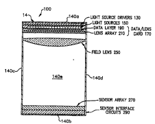
As shown in Figure 1, the data layer 190 for storing
optical data is formed as part of a data/lens card 170 which
incuL~ol~tes, in accordance with the present invention, a
simplex lens array 210 that is characterized by a single
diffractive element or surface for each page of data to be
imaged on sensor array 270. This single diffractive element,
one per data page, collects data image light created by
energi~ing one of multiple light sources (omitted in Figure 1
but shown in the _ _let~ memory apparatus of Figure 7a) and
causes the image rays to be pLucessed for creating an image on
~ensor arr~y 270 through an intervening field lens 250 that is
common to all of the data pages in layer 190 and all of the
diffractive simplex elements of array 210. Other than the
unique optical and structural characteristics of the simplex
lens array 210 of the present invention, the basic
construction and operation of the optical random access memory
shown in Figure 1 and more completely in the apparatus of
Figure 7a and 7b, are ~; ~rl osed in related co-pending U.S.
Patent ~pplirnt;rn Serial No. 07/815,924 and international
Patent Application Serial No. PCT/US92/11356, the pllhl;~hr~
sprr;f;rntions of which are incuL~uLated herein by reference.
~ W096/02057 2 19 ~ 2 8 3 r~l,u~sl~ ~Y
Thus, as in the above mentioned related applications,
. ~ ~
data/lens card 170 i5 constructed as a unitary e L
formed by bonding together the various layers ;n~ ing the
data layer 190 and, in this case, the simplex diffractive lens
array 210, 80 that card 170 i8 removable and rPpl~P~hle by
other like constructed data cards for storing different data,
into the memory 100 shown in Figure 7a.
Unique to the present invention is the economy of
manufacturing data/lens card 170 with an array 210 which has
but one surface, that being diffractive, for each of the data
pages. As ~;~cn~sP~ in greater detail below, the present
invention is capable of resolving the relatively dense data on
layer 190 by using a spPc;~lly constructed grating that forms
the diffractive surface of lens array 210 and by requiring
that the data bits or spots on the data layer 190 be
configured 80 as to produce a certain light dispersion
envelope that co-functions with the spP~;~lly configured
diffractive grating on the lens element to differentially
reject light rays from the data layer that are not capable of
being focused sharply on sensor array 270.
To better underst~nd the structural and optical
requirements of the data/lens card 170 in accordance with the
present invention, reference is made to Figures 3a, b and c,
and 4a, b and c, showing respectively the data layer and the
configuration of the patches or data pages, and the simplex
diffractive element or surface, ;nrlll~;ng the ovPrl~pr;ng
concellLLic grating patterns and specially configured grating
grooves. Thus, in Figure 3a, the data layer 190 is organized
W096/020S7 P~~ /Y
2~9~2&3 ~
into a large num~er of data pages 195, here in the form of
roughly hexagonal or circular cells closely packed for
m-~;m; 7i ng page and hence data density. Figure 3b
illustrates, but at a much lower density than in actual
practice, the individual data bits, here in the form of spots
or holes in a phof~hPm;~A1 film for representing binary data.
An open hole represents a binary bit "1"; a closed hole
s~-lLs the bit 0 . The data bits are as densely packed
~8 can be resolved by the optics and, in this case, the data
holes of diameter dl = 0.9 microns at a spacing of d2 = 1.5
microns as shown in the cross-section of Figure 3c. These
data holes are furth~ selected as ~c~rihed below 80 that
the dispersion envelope of light from a light source having a
plane wavefront that coacts with an aspect ratio of depth to
15 width of the grating grooves on the diffractive layer creates
a virtual or arfifiriAl stop in the overall optical imaging
system of Figure 1 that yields a highly resolved sharp image
of the data layer on sensor array 270.
Thus with reference to Figures 4a, 4b and 4c, the simplex
20 diffractive grating layer 230 has overlapping circular
gratings that form a dif~ractive element 215, one for each of
the data pages 195 and in axial registration therewith. The
overlapping of the gratings is exaggerated for illustration in
Figures 4a and 4b, but some overlap is needed because the
25 light rays, as they propagate from the data layer 190 shown in
Figure 1, veer off axis and into a neigh~ring diffractive r
lens element 215 due to the close pack pages 195 of data layer
190. Although not discernible from Figure 4c, the grating
WO 96102057 I'~ S. 1~
~ 2~ ~42~3
pattern of each of the diffractive lens elements 215 has a
selected minimum depth to width aspect ratio in the grating
groove that is critical to the present invention and is
~ discussed more fully in connection with Figure 5.
While it i8 not possible to place a real physical stop at
a location beyond the image in order to optimize the sharpness
of the image, it i8 ~Lu,uosed in accordance with the present
invention to achieve the same or similar result by creating an
ar~;fir;~l stop by other optical structure to control the way
that the bundles of data rays intersect with the diffractive
lens element. More sp~rifirAlly, and as best illustrated in
Figure 5, the simplex diffractive lens 215 for a single page
195 is preferentially illnmin~ted on the same side of the
center line or axis 217 of the lens as the data point that is
to be imaged. In the preferred '-'i L this i8 in part
achieved by using a hole size for each data bit that causes,
in conjunction with the predet~rmined wavelength A of the
source light, an output distribution envelope or intensity
profile 219 that restricts the div~Ly~llce and direction of the
light to attenuate or minimi~e those "bad" rays that would
diverge and i~ min~te the lens on the other side of the axis
217 from the originating data bit. In other words, any light
following ray path 221 as shown in Figure 5 would be first
attenuated or min;m;~d by the intensity envelope 219 in
~rc~r~nre with the following function:
w096l02057 F~~ /Y
21 94283 ~
sin n-d, sin(x~ 2
f(x) = ~ (1 + CO8(X) )2
n d. sin~xi 2
A
n n n
x = -- , -- _ + .01. . .
-2 2 2
and A= 0.645 microns
10dl= 0.9 microns
This function defines the intensity of the envelope
originating at a point source and is a function of the
wavelength A of the light source, and the diameter of the data
hole. In this : ' 'i L, a wave length of 0.645 microns i8
u~ed as the source light and a data hole in page 195 is 0.9
microns. It is obs~Lv.2d that the intensity envelope
~;gn;fir~ntly attenuates light rays that diverge from the
point source at an angle that in the extreme bit poc;~;~n of a
data page would pass through the diffractive lens element 215
on the other side of center line 217. It is ~uch diverging
rays such as illustrated by dotted line 221 that are to be
discriminated against in order to optimize the resulting image
on the sensor array.
~ second optical feature of the preferred ~ is
to fabricate the 3implex diffractive lens 215 with a grating
groove pattern 223 that, as shown in Figure 5, has a greater
depth than width aspect ratio and this ratio is preferably at
least 3:1. Thus the three ~; c;~n~l gf LLY of grating
grooves 223 with a depth to width ratio as sp~; f; ed, creates
an acceptance angle that ~;C~r;~in~tes against the divergent
bad rays such as indicated by ray path 221 as shown in Figure
5. While the aspect ratio of grooves 223 can be in the range
12
WO96/02D57 2 ~ 9 4 2 ~ 3 ~ ~ I r ~ ~ ~Y
of 1:1 to 4:1 or more ~p~n~ing upon the difference in the
index of refraction from the transparent bonding ~-t~ni~1 of
the card through the material of diffractive lens 215, a
preferred aspect ratio is as mentioned of D to W equal to or
greater than 3:1. This diffraction groove aapect ratio
cooperates with the elongated intensity profile of the bit
hole light to further ~ic~nim;n~te against and hence attenuate
those bad light rays that if allowed to reach the sensor image
plane would make an aberrated image and cause errors in the
data readout.
Figure 6 is a computer generated view of the imaging
effect of a single diffractive lena element 215 prscescing
data bits on a page 195 consiating of a center bit and two
extreme bits. In this illustration, the field lens has been
omitted in order to more clearly show the crossing of the
bundles of light rays from the extreme bit l~a~;nnc as they
are ~Loces3ed by the simplex diffractive lens 215. It will be
nppreciated that in both the illustration in Figures 5 and 6,
the complete operating optical random access memory has an
array of pagea 195 and a coLL~ullding array of diffractive
lenslets or lens 215 each in effect forming a layer of the
sandwich data/lens card 170 as depicted in Figures 1 and 7a.
Now with reference to Figures 7a, and the associated
addressing and control electronics in Figure 7b, the operation
of the memory 100 is ~c~rih~ in detail in the above
mentioned cop~n~; ng U.S. Patent Application Serial No.
07/815,924 and international Patent Application Serial No.
PCT/US92/11356. The addressing electronics 290 may be
13
W096/020~7 Y~~ ( /9
21 94283
integrated into a flat substrate and mounted as shown in
Figure 7a for Arc~sing data from ORAM 100 by accepting
~ddressing data from a data bus 121 connected via an interface
bus 123 through an address buffer 125 to select particular
rows of data after an image has been formed on sen30r array
270. ~his is done by operating row select switches 127. To
;llnmin~te a gelected data page, the address available from
bua 121 ;nrlnA~s page address data fed over x and y decode
buses 131 and 133 which cause x decode 135 and y decode 137 to
select a particular one of the multiple light source drivers
130 of sources 150 to ill nmi nAte a single page 195 of data for
imaging onto sensor array 27. A timing control 139 provides
in a manner known per se, a sequence of timing control signals
identified as "pulse LYD" (controls page light drivers source
130); "pulse CCD row" (controls the read-out of data from a
charge coupled device sensor array 270); gate MUX" (controls
an output multiplexer from sensor array 270); and "data ready"
(signals that the data is ready from the data output
multipl~Y~r and interface to a data user bus). The output of
data from sensor array 270 is made available through a buffer
register 141, a multiplexer 143, an interface to bus 145, and
an output data bus 147.
While only particular e ' 'i Ls have been ~ los~d
herein, it will be readily apparent to persons skilled in the
art that numerous changes and 'i f i ~ation8 can be made
thereto, in~ ing the use of equivalent means, devices, and
method steps without departing from the spirit of the
invention.