Note: Descriptions are shown in the official language in which they were submitted.
WO 96/04572 2~ 94569 PCT/6B95/01724
i
1
IONIZING RADIATION DETECTOR
The present invention relates to an ionizing
radiation detector, and in particular to a detector
suitable for detecting high energy radiation and/or
charged or neutral particles.
A typical prior art detector is shown in Figure 1.
The detector comprises a flat sheet 10 of an insulating
material such as diamond, having thin gold electrode
coatings 12,14 on its upper and lower surfaces. The
upper electrode coating 12 comprises a plurality of
parallel readout strips which are aligned in a direction
perpendicular to the plane of the paper in the Figure,
and the lower electrode coating 14 comprises a further
plurality of readout strips _aligned in a direction
parallel with the plane of the paper. A large potential
difference V is maintained between the electrode
coatings.
A charged particle following a path 16 through the
diamond produces electron-hole pairs 18,20, which
separate under the influence of the electric field and
induce a charge on the readout strips. The energy of the
particle can be determined by the amount of charge which
is collected, and its position by the intersection of the
upper and lower strips receiving the largest induced
charges.
There are a number of disadvantages with this type
of detector, in particular its relatively poor charge
collection efficiency. The charge collection efficiency
is typically limited by the charge intrinsic life time
within the diamond, and this can only be made large if
expensive diamond is used, having a large recombination
length. In addition, the accuracy with which the
particle can be located in the x-y plane is limited by
WO 96/04572 21 ,9 4569 PCT/GB95/01724
2
the inevitable cross-talk between the readout channels.
Finally, the detector is sensitive to particles coming in
from a wide range of angles, which means that it is not
particularly suited for imaging purposes. If imaging is
to be required, it is normally necessary to incorporate
a collimator in front of the detector to ensure that
particles travelling at an angle to the normal to the
detector surface are weeded out. Such collimators not
only add to the cost of detection equipment, but also
limit its sensitivity.
in an effort to improve detection efficiency, and to
avoid the use of collimators, there have been a number of
proposals to provide detectors which are deep in
comparison with their width. Typically, a bundle or
stack of several of these individual detectors are used
together. Examples are shown in US-A-4891521 and GB-A-
1559664. The devices shown in both of these documents
appears to be specifically intended for high-rate data
taking. The present invention, on the other hand, is
concerned with providing a device which is at least in
principle capable of extremely high time resolution and
spatial resolution when detecting an individual event.
It is an object of the present invention at least to
alleviate the problems of the prior art.
According to the present invention there is provided
an ionizing radiation detector comprising a single wafer
of a detector material, the wafer having a plurality of
parallel sided grooves in a surface thereof thereby
defining between the grooves a plurality of parallel
sided detector elements, opposing sides of each element
carrying opposing readout electrodes; and means for
applying a potential difference between the opposing
electrodes of each element to create an electric field
across the element.
WO 96/04572 2 1~ ~ 50 PCT/GB95101724
~ 3
Also according to the present invention there is
provided an ionizing radiation (or photo) detector
comprising a substrate and a plurality of detector
elements, having generally parallel sides, extending
outwardly from a surface of the substrate, the sides
carrying readout electrodes.
Such detectors of the present invention have many
advantages, particularly for the construction of the type
of detector working on the photoconducting principle.
They are relatively cheap to manufacture, they can
provide high sensitivity, extremely fast readouts, and
they can provide very accurate positioning information
with minimal cross talk between channels. It is
anticipated that detectors of this type will find a
multitude of uses, including medical imaging, high energy
particle physics, combustion and plasma physics, ultra-
violet detectors for use in astronomy and so on.
The size of the detector elements determines the
ultimate resolution, the resolution being limited in the
present invention merely by limitations in the
fabrication process. Detector elements can be
manufactured, for example by laser etching techniques,
having a width of 10 micrometres or more. For optimal
readout speed, it is preferred that the width of the
detector elements be less than the recombination length
of the material from which the detector elements are
manufactured, so that a large proportion of the ionised
electrons/holes reach the electrodes. The exact
preferred width of the elements will of course depend
upon the material used, but typically the width is likely
to be between 20 and 100 m. For special uses it would
be possible to build devices having gaps between the
ridges of as little as 1 m; however, as this would
require the use of ion beams the resultant device would
~
WO 96104572 2194569 PCT/GB95/01724
$ ~
inevitably be expensive.
The detector may be made from diamond, either
natural or artificially grown. The diamond, if
artificially grown, is preferably intrinsic (that is, not
doped). Suitable diamond growing techniques include CVD
(chemical vapour deposition) and plasma enhanced CVD.
These can be used as detectors for particles with energy
from a few eV upwards. A typical characteristic of this
type of diamond is that the carrier recombination length
is small compared with that obtained in natural type IIA
diamonds. The small recombination length normally
results in poor collection of the charge carriers
produced by an incoming particle in a detector of
traditional design. The proposed detector geometry,
however, enables the lateral dimension (width) to be
sufficiently small to match the micrometre-size
recombination length of standard grown diamond, without
the need for expensive techniques to improve the quality
of the diamond to increase the recombination length.
Accordingly, the detector of the present invention is
able to make use of relatively cheap, poor quality grown
diamond (for example 6 m recombination length) which at
present is less desirable for use in detectors. It may
also use slightly higher quality diamond (but still not
of the highest quality) of between 80 and 100 m
recombination length.
Alternatively, the detector may comprise silicon or
GaAs, for example a single wafer of either of these
substances.
Preferably, the height of each detection element,
measured in a direction parallel to its sides, is
relatively large in comparison with its width, defined as
the distance between the parallel sides. The aspect
ratio (height/width ratio) is preferably at least as high
WO 96/04572 219 4 5 6 9 PCT/GB95/01724
as 10, and may be as much as 100 depending upon the
application. The use of high aspect ratios enable
detectors embodying the present invention to exhibit both
high sensitivity (because a particle being detected
traverses the entire length of the detector element) and
high speed (because the electrons/hole carriers only have
a very short distance to travel be-fore they reach the
nearest electrode.
The greater the aspect ratio, the greater will be
the directional sensitivity of the device. With large
aspect ratios, it is possible to do away entirely with
the collimators which are frequently found to be
necessary with prior art detectors used in imaging
applications. The device of the present invention should
both be -directional enough, and spatially accurate
enough, to provide imaging without the use of separate
collimators, given an appropriate disposition of detector
elements, for example upper and lower orthogonal ridges
as described below. The ridge length is preferably large
in comparison with the ridge height and width.
It will be appreciated, of course, that the
invention is not restricted to devices having detection
elements which are higher than they are wide. Likewise,
the invention is not restricted to any particular
relationship between the spacing between the detector
elements and the widths of the elements themselves. In
some embodiments, it might be preferable to have very
narrow spaces between the elements (compared with the
widths of the elements themselves); in other embodiments
it might be preferable for the spacing between the
elements to be wider than the widths of the elements
themselves.
The detector preferably comprises a generally flat
wafer, with detector elements extending outwardly in a
WO 96/04572 21945" 9 PCT/GB95101724
6
direction generally perpendicular to the plane of the
wafer. In use, the detector is designed to be positioned
so that the incoming particle or radiation beam being
detected is normal to the plane of the wafer. In one
preferred embodiment, the detector elements comprise a
plurality of parallel ridges, etched, grown or otherwise
formed in the front surface of the wafer. Where location
in two dimensions is required, the wafer may be double-
sided with a first series of parallel ridges on one side,
and a second orthogonal series of parallel ridges on the
other side. Two sets of readout devices may be provided
so that the upper surface provides x position information
and the lower surface y position information.
Where the detector elements comprise a plurality of
parallel ridges, the lateral electrodes will produce a
relatively large capacitative effect. This can be
largely eliminated by arranging to match the impedance of
each pair of electrodes with the impedance of the readout
devices at the ends of the ridges (wires, amplifiersand
so on). Effectively, what one is doing is treating the
readout electrodes as transmission lines and matching the
impedance of those transmission lines. This results in
very much faster signal processing, and substantially
reduced signal loss.
Depending upon the exact configuration, in
particular the material of which the detector is made and
the aspect ratio, various types of particle may be
detected. Specifically, detectors embodying the present
invention could be used for all types of charged particle
detection and for photons. To obtain a greater signal
strength when photons are to be detected, a layer of
high-Z material may be placed on top of the detector
elements to cause showering. Since the showering layer
is immediately in front of the detector elements, very
WO 96104572 21/45U 7 PCT/G895/01724
~ 7
little additional cross-talk is introduced. With high
aspect ratios, efficient gamma rays detection can also be
achieved; self-collimation is critical here, since
normal collimators generally lose too large a proportion
of the sample. The detection of neutral particles such
as neutrons may be enhanced by filling the spaces between
the detector elements with an absorber material, such as
a plastics material.
According to a further aspect of the invention there
is provided an ionizing radiation (photo) detector
comprising a plurality of detector elements having
parallel sides, the sides carrying readout electrodes,
the detector being arranged to operate with the
electrodes parallel to an incoming particle or radiation
beam to be detected.
Preferably, the height of the detector elements, in
a direction perpendicular to the incoming beam, is
relatively large in comparison with the width, defined as
the distance between the parallel sides.
With at least certain embodiments of the present
invention it is expected that charge readout times will
be less 50 ps, probably less than 35 ps.
The invention may be carried into practice in a
number of ways and several specific embodiments will now
be described, by way of example, with reference to the
drawings, in which:
Figure 1 shows a prior art detector;
Figure 2 is a cross-section through a detector
embodying the present invention;
Figure 3 is a perspective view of the detector of
Figure 2;
Figure 4a shows another embodiment, the electrodes
being connected in a bipolar voltage configuration;
Figure 4b shows the embodiment of Figure 4a, the
2194569 WO 96/04572 PCT/GB95101724
8 *
electrodes being connected in a resistor chain
configuration; and
Figure 5 shows yet a further embodiment.
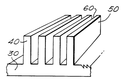
The preferred detector of the present invention is
illustrated in Figures 2 and 3. it is a diamond detector
and comprises a diamond substrate 30 having, on one
surface, a plurality of parallel etched diamond ridges
40. on one side of each ridge there is a positive
readout electrode 50, and on the other side a negative
electrode 60. These are preferably conductors, but
could instead be of a high-conductivity doped semi
conductor material.
In use, the detector is positioned so that the
substrate lies substantially normal to a particle or
- radiation beam 70 to be detected. An individual particle
passing into one of the ridges creates ionised carriers,
which rapidly migrate to the electrodes 50,60 by virtue
of the large potential difference which is maintained
between them. Charge is thereby induced on the
electrodes, this charge being read off by readout devices
(not shown) at the ends of the ridges.
The substrate and the ridges are preferably of
diamond, which may either be natural or artificially
grown. The ridges may either be grown, with the
substrate, or they may be etched (for example with an
eximer laser) The electrodes 50,60 may be of any
suitable ohmic material, such as gold, tungsten, titanium
and so on. Standard deposition techniques may be used to
apply the metal as a thin coating to the sides of the
ridges. Typically, the device may be made by etching
the ridges, depositing the material, and then polishing
the top surface.
It will be appreciated from Figure 2 that the
sensitivity of the device shown can be increased by
21.94569
WO 96/04572 PCT/GB95/01724
~ 9
making the value of D (or the height of the ridges)
larger. The greater the height of the ridges, the larger
the amount of material which a particle has to pass
through, thereby increasing the ionisation within the
device. The height of the ridge will normally be matched
to the expected penetration depth of the particles to be
detected. The readout speed and efficiency is determined
by the width L of each of the ridges. Depending upon
the particular application, the value of L may be as
little as a few micrometers, or a larger value up to
about 200 m, and the value of D 10 m or more. The
signal-to-noise ratio is large, as there is negligible
cross-talk between signals emanating from individual
ridges. A typical substrate depth is around 100 {im,
sufficiently thick to support the ridges and to be free-
standing without requiring an additional supporting base.
Preferably, the device ma7ces use of relatively poor
quality diamond, having a recombination length of perhaps
6 }cm or so.
The impedance of the readout devices (not shown) at
the end of the ridges is preferably matched with the
impedance of the electrodes 50,60, thereby increasing
readout speed and reducing.signal losses.
There are a number of ways in which a potential
difference may be applied between the electrodes 50,60
shown in Figure 2. In its simplest form, a voltage
source may simply be connected between the two
electrodes. Alternatively, the electrodes may be coupled
to a resistor chain (not shown), the potential difference
between the electrodes thereby being defined by the
potential drop across the corresponding resistor.
Another embodiment is shown in Figure 4, in which
the electrodes are formed over-the base and the sides of
the space between the diamond ridges 40. This means,
WO 96/04572 219-T 567 PCT/GB95101724
effectively, that each electrode 50' on the left side of
a ridge 40 is electrically coupled with a corresponding
electrode 60' on the right hand side of the next ridge in
the sequence so that they together form a single U-shaped
5 electrode 61. In the embodiment of Figure 4a, first
alternate pairs of U-shaped electrodes 61 are coupled via
a first voltage source Võ and second alternate pairs are
coupled by a second voltage source V2. Such a bipolar
voltage configuration ensures that there is always a
10 constant potential difference V1 - V2 across each of the
ridges 40.
An alternative method of applying voltages to the U-
shaped electrodes 61 is shown in Figure 4b. Here, a
resistor chain is used to drop an input voltage V across
a plurality of series resistors R. The voltage across
each ridge 40 :may be chosen by selecting appropriate
values for V and R.
It will be understood, of course, that a similar
bipolar voltage configuration or resistor chain voltage
configuration may be used in conjunction with the
embodiment of Figure 2.
A typical pote.ntial difference across the ridge 40
may be in the region of 1 volt per pm. Substantially
higher voltages could be used, if desired (since diamond
has a very high breakdown potential), but there is
generally no need for high potential differences since at
greater voltages the carrier speed rapidly saturates.
In a further embodiment (not shown) a further
parallel set of ridges, orthogonal to the first set, is
provided on the lower surface of the substrate 30. These
two perpendicular sets of ridges allow accurate x-y
positioning of each detected particle.
The spaces between the ridges may be filled with a
plastics material, or other absorber, thereby improving
CA 02194569 2006-04-07
67573-11
11
the capability of the detector to detect neutral particles.
Yet a further embodiment is shown in Figure 5.
Here, the spaces between the ridges 40 have become extremely
narrow, and they each contain a separate electrode 62. Such
an embodiment is, in many circumstances, preferred since the
narrowness of the gaps between the ridges 40 produces only a
small acceptance loss compared with the embodiments of
Figures 2, 3 and 4. The width of the gap, and hence the
width of the electrode 62, may depend primarily on how
narrow a slot can be cut into the diamond substrate. The
electrodes 62 may be coupled together in any convenient
manner so as to produce a suitable potential difference
across the ridges 40, for example using the approach of
Figure 4a or of Figure 4b.
The detection of high energy electromagnetic
radiation, such as gamma rays, may be improved by adding a
showering layer (not shown) on top of the ridges. An
incoming photon first strikes the showering layer, and the
resulting shower then penetrates into one of the ridges
below, providing a signal which can be detected.
The ionizing radiation detector described above
can provide extremely rapid charge readout, probably within
35 ps and certainly within 50 ps. These readout speeds
cannot currently be achieved for any single pulse detector
of comparable sensitivity and positional accuracy.