Note: Descriptions are shown in the official language in which they were submitted.
2194711
~..
Method and Apparatus for Improved Coin, Bill
and Other Currency Acceptance and Slug or
Counterfeit Rejection
This is a division of copending Canadian Patent
Application Serial No. 2,069,875 filed on May 28, 1992,
based on PCT/US91/07548 filed October 9, 1991.
Technical Field
The present invention relates to the
examination of coins, bills or other currency for purposes
such as determining their authenticity and denomination,
and more particularly to methods and apparatus for
achieving a high level of acceptance of valid coins or
10 currency while simultaneously maintaining a high level of
rejection of nonvalid coins or currency, such as slugs or
counterfeits. While the present invention is applicable
to testing of coins, bills and other currency, for the
sake of simplicity, the exemplary discussion which follows
15 is primarily in terms of coins. The application of the
present invention to the testing of paper money, banknotes
and other currency will be immediately apparent to one of
ordinary skill in the art.
Backqround Art
It has long been recognized in the field of
coin and currency testing that a balance must be struck
between the conflicting goals of "acceptance" and
'~rejection"--perfect acceptance being the ability to
correctly identify and accept all genuine items no matter
25 their condition, and perfect rejection being the ability
to correctly discriminate and reject all non-genuine
items. When testing under ideal conditions, no difficulty
arises when trying to separate ideal or perfect coins from
slugs or counterfeit coins that have different character-
30 istics even if those differences are relatively slight.
Data identifying the characteristics of the ideal coins
2194711
--2--
can be stored and compared with data measured
from a coin or slug to be tested. By narrowly
defining coin acceptance criteria, valid coins
that produce data falling within these criteria
can be accepted and slugs that produce data
falling outside these criteria can be re~ected.
A well-known method for coin acceptance and
slug rejection is the use of coin acceptance
windows to define criteria for the coin
acceptance. One example of the use of such
windows is described in U.S. Patent Nos.
3,918,564 and 3,918,565, both assigned to the
assignee of the present invention.
Of course, in reality, neither the
test conditions nor the coins to be tested are
ideal. Windows or other tests must be set up
to accept a range of characteristic coin data
for worn or damaged genuine coins, and also to
compensate for environmental conditions such as
extreme heat, extreme cold, humidity and the
like. As the acceptance windows or other coin
testing criteria are widened or loosened, it
becomes more and more likely that a slug or
counterfeit coin will be mistakenly accepted as
genuine. As test criteria are narrowed or
tightened, it becomes more likely that a
genuine coin will be rejected.
U.R. Application Serial No. 89/23456.1
filed Oct. 18, 1989, and assigned to the
assignee of the present invention, is one
response to the real world compromise between
achieving adequately high levels of acceptance
and rejection at the same time. This U.K.
application describes techniques for
establishing non-uniform windows that maintain
a high level of acceptance while achieving a
high level of rejection.
Another prior art approach is found in
the Mars Electronics IntelliTrac~ Series
products. The IntelliTrac Series products
194711
-- 3
operate substantially as described in European Patent
Application EP 0 155 126, which is assigned to the
assignee of present invention.
SUMMARY OF THE INVENTION
In accordance with one aspect of the invention
there is provided a method of operating a money validation
apparatus which compares at least one output signal
generated by a sensor in response to an inserted item to
at least one predetermined acceptance window to validate
the item, wherein the acceptance window is defined by a
range of values between a reference value and a first
acceptance boundary, comprising: setting a deviation
limit between the reference value and the first acceptance
boundary; accepting an inserted item as genuine money if
the output signal is within the acceptance window; and
modifying the acceptance window if a predetermined number
of accepted items had output signals falling within the
deviation limit.
In accordance with another aspect of the
invention there is provided a method of operating a money
validation apparatus which utilizes acceptance criteria
corresponding to genuine items of different types, wherein
the acceptance criteria is comprised of characteristic
data having a center point, comprising: setting a
deviation limit which is small in comparison to the
distance from the center point to a boundary of the
acceptance criteria; testing an item and generating
characteristic data for the item; accepting the item as
being of a particular type if its characteristic data is
within the acceptance criteria corresponding to that type;
calculating the absolute difference between the character-
istic data of the accepted item and the center point of
the acceptance criteria; adding the difference of the
center point and the~ data of the accepted item to a
cumulative sum if the absolute difference is less than or
equal to the deviation limit; incrementing the center
point of the acceptance criteria by a preset amount when
the cumulative sum exceeds a predetermined limit, or
decrementing the center point by a preset amount when the
219~711
-- 4
cumulative sum is less than a predetermined negative
limit; and resetting the cumulative sum.
In accordance with yet another aspect of the
invention there is provided a money validation apparatus
having a means for comparing tested item data to item
acceptance criteria corresponding to genuine items of
different types, wherein each item acceptance criteria has
a center point, comprising: means for setting a deviation
limit which is smaller than the distance from the center
point to a boundary of the acceptance criteria; means for
testing an item and generating characteristic data; means
for accepting the item if its characteristic data is
within the acceptance criteria; means for calculating the
absolute difference between the accepted characteristic
data and the center point; means for adding the difference
of the accepted item characteristic data and the center
point to a cumulative sum if the absolute difference is
less than or equal to the deviation limit; means for
incrementing the center point by a preset amount when the
cumulative sum is greater than a predetermined limit, or
decrementing the center point by a preset amount when the
cumulative sum is less than a predetermined limit; and
means for resetting the cumulative sum.
The present invention can be applied to a wide
range of electronic tests for measuring one or more
parameters indicative of the acceptability of a coin,
currency or the like. The various aspects of the
invention may be employed separately or in conjunction
depending upon the desired application.
Brief Description of the Drawinqs
The present invention taken in conjunction with
the invention disclosed in copending Canadian Patent
Application Serial No. 2,069,875 filed on May 28, 1992,
based on PCT/US91/07548 filed October 9, 1991, will be
described hereinbelow with the aid of the accompanying
drawings in which:
Fig. 1 is a schematic block diagram of an
embodiment of electronic coin testing apparatus, including
sensors, suitable for use with the invention;
219~711
-
- 4a -
Fig. 2 is a schematic diagram indicating
suitable positions for the sensors of the embodiment of
Fig. 1;
Fig. 3 is a graphical representation of a prior
art coin acceptance window for testing three coin
acceptance criteria;
Fig. 4 is a graphical representation of one
aspect of the present invention, namely improved coin
acceptance criteria using coin acceptance clusters;
Fig. 5 is a flow chart of the operation of the
coin acceptance clusters for the improved definition of
coin acceptance criteria of the present invention;
Fig. 6 is a graphical representation of a
typical line distribution curve of certain measured
criteria for a genuine coin;
Fig. 7A is a graphical representation of the
line distribution for the genuine coin criteria of Fig. 6
drawn to include a line distribution for the same criteria
of an invalid coin, to illustrate the anti-fraud or anti-
cheat aspect of the present invention;
Fig. 7B is an additional graphical
representation showing substantial overlap for certain
measured criteria of a genuine coin line distribution and
an invalid coin line distribution;
Figs. 7C and 7D are additional graphical
representations showing minimal overlap for certain
measured criteria for certain genuine coin
219~711
line distributions and invalid coin line
distributions;
~ig. 8 is a flow chart of the operation
of the anti-fraud or anti-cheat aspect of the
present invention;
~ig. 9 is a flow chart of the operation
of the zspect of the present inventi,on relating to
minimizing the effects of counterfeit coins and
slugs on the self-adjustment process for the
center of the coin acceptance window;
~ig. 10 is a flow chart of a portion of
the operation of the present invention relating to
relative value computation and conservation of
memory space and minimization of microprocessor
computation time in a microprocessor based coin
validation system; and
Fig. 11 i5 a graphical representation
concerning that aspect of the present invention
describing the m~dification of the measured
response in the validation apparatus due to the
presence of large changes to the reference
parameter; Fig. 11 is located on the same sheet
of drawings containing Figs. 6 and 7A.
Detailed Description
2S The coin examining apparatus and methods
of this invention may be applied to a wide range
of electronic coin tests for measuring a parameter
indicative of a coin's acceptability and to the
identification and acceptance of any number of
3~ coins from the coin sets of many countries. In
particular, the following description concentrates
on the details for setting the acceptance limits
for particular tests for particular coins, but the
application of the invention to other coin tests
and other coins will be clear to those ~killed in
the art.
2194711
-6-
The figures are intended to be
representational and are not drawn to scale.
Throughout this specification, the term ~coin~ is
intended to include genuine coins, tokens,
counterfeit coins, slugs, washers, and any other
item which may be used by persons in an attempt to
use coin-operated devices. Also, th,e disclosed
invention may suitably be applied to validation of
bills and other currency, as well as coins. It
will be appreciated that the present invention is
widely applicable to coin, bill and other currency
testing apparatus generally.
The presently preferred embodiment of the
method and apparatus of this invention is
implemented as a modification of an existing
family of coin validators, the Mars Electronics
IntelliTrac Series. The present invention employs
a revised control program and revised control
data. The IntelliTrac Series operates
substantially as described in European Application
EP 0 155 126.
Fig. 1 shows a block schematic diagram of
a prior art electronic coin testing apparatus 10
suitable for implementing the method and apparatus
of the present invention by making the
modifications described below. The mechanical
portion of the electronic coin testing apparatus
10 i~ shown in Fig. 2. The electronic coin
testing apparatus 10 includes two principal
sections: a coin examining and ~ensing circuit 20
including individual sensor circuits 21, 22 and
23, and a processing and control circuit 30. The
processing and control circuit 30 includes a
programmed microprocessor 35, an analog to digital
(A/D) converter circuit 40, a signal shaping
2194711
circuit 45, a comparator circuit 50, a counter 55,
and NOR-gates 61, 62, 63, 64 and 65.
Each of the sensor circuits 21, 22
includes a two-sided inductive sensor 24, 25
having its series-connected coils located adjacent
opposing sidewalls of a coin passageway. As shown
in Fig. 2, ~ensor 24 is preferably of a large
diameter for testing coins of wideranging
diameters. Sensor circuit 23 includes an
inductive sensor 26 which is preferably nrranged
as shown in Fig. 2.
Sensor circuit 21 is a high-frequency,
low-power oscillator used to test coin parameters,
such as diameter and material. As a coin passes
the sensor 24, the frequency and amplitude of the
output of sensor circuit-21 change as a result of
coin interaction with the sensor 24. This output
is shaped by the shaping circuit 45 and fed to the
comparator circuit 50. When the change in the
amplitude of the signal from shaping circuit 45
exceeds a predetermined amount, the comparator
circuit 50 produces an output on line 36 which is
connected to the interrupt pin of microprocessor
35.
The output from shaping circuit 45 is
also fed to an input of the A/D converter circuit
40 which converts the analog signal at its input
to a digital output. This digital output is
serially fed on line 42 to the microprocessor 35.
The digital output is monitored by microprocessor
35 to detect the effect of a passing coin on the
amplitude of the output of sensor circuit 21. In
conjunction with frequency shift information, the
amplitude information provides the microprocessor
35 with adequate data for particularly reliable
testing of coins of wideranging diameters and
materials using a single sensor 21.
219~711
--8--
The output of sensor circuit 21 is also
connected to one input of NOR gate 61 the output
of which is in turn connected to an input of NOR
gate 62. NOR gate 62 is connected as one input of
NOR gate 65 which has its output connected to the
counter 55. Freguency related information for the
sensor circuit 21 is generated by selectively
connecting the output of sensor circ'uit 21 through
the NOR gates 61, 62 and 65 to the counter 55.
Frequency information for ~ensor circuits 22 and
23 is similarly generated by ~electively
connecting the output of either sensor circuit 22
or 23 through its respective NOR gate 63 or 64 and
the NOR gate 65 to the counter 55. Sensor circuit
22 is also a high-frequency, low-power oscillator
and it is used to test cDin thickness. Sensor
circuit 23 is a strobe sensor commonly found in
vending machines. As shown in Fig. 2, the sensor
26 is located after an accept gate 71. The output
of sensor circuit 23 is used to control such
functions as the granting of credit, to detect
coin jams and to prevent customer fraud by methods
such as lowering an acceptable coin into the
machine with a string.
The microprocessor 35 controls the
selective connection of the outputs from the
~ensor circuits 21, 22 and 23 to counter 55 as
described below. The frequency of the oscillation
at the output of the sensor circuits 21, 22 and 23
is sampled by counting the threshold level
crossings of the output signal occurring in a
predetermined sample time. The counting is done
by the counter circuit 55 and the length of the
predetermined sample time is controlled by the
microprocessor 35. One input of each of the NOR
gates 62, 63 and 64 i5 connected to the output of
its associated sensor circuit 21, 22 and 23. The
2194711
output of sensor 21 is connected through the NOR
gate 61 which is connected as an inverter
amplifier. The other input of each of the NOR
gates 62, 63 and 64 is connected to its respective
control line 37, 38 and 39 from the microprocessor
35. The signals on the control lines 37, 38 and
39 control when each of the sensor circuits 21, 22
and 23 is interrogated or sampled, or in other
words, when the outputs of the sensor circuits 21,
22 and 23 will be fed to the counter 55. For
example, if microprocessor 35 produces a high
(logic ~1~) signal on lines 38 and 39 and a low
signal ~logic ~o~) on line 37, sensor circuit 21
is interrogated, and each time the output of the
NOR gate 61 goes low, the NOR gate 62 produces a
high output which is fed through NOR gate 65 to
the counting input of counter 55. Counter 55
produces an output count signal and this output of
counter 55 is connected by line 57 to the
microprocessor 35. Microprocessor 35 determines
whether the output count signal from the counter
55 and the digital amplitude information from A/D
converter circuit 40 are indicative of a coin of
acceptable diameter and material by determining
whether the outputs of counter 55 and A/D
converter circuit 40 or a value or values computed
therefrom are within stored acceptance limits.
When sensor circuit 22 is interrogated,
microprocessor 35 determines whether the counter
output is indicative of a coin of acceptable
thickness. Finally, when sensor circuit 23 is
interrogated, microprocessor 35 determines whether
the counter output is indicative of coin presence
or absence. When both the diameter and thickness
tests are satisfied, a high degree of accuracy in
discrimination between genuine and false coins is
achieved.
-- 219~711
--10--
A person skilled in the art would readily
be able to implement in any number of ways the
specific logic circuits for the block diagram set
forth in Fig. 1 and described above. Preferably,
S the circuitry suitable for the embodiment of Fig.
1 is incorporated in an application specific
integrated circuit (ASIC) of the type presently
part of the TA100 ~tand alone acceptor sold by
Mars Electronics, a subsidiary of the assignee of
the present invention. Another ~pecific way to
implement the circuitry of Fig. 1 is shown and
described in European Patent Application EP 0 155
126, referenced above, which is assigned to the
assignee of the present invention.
The methods of tne present invention will
now be described in the context of setting coin
acceptance limits based upon the frequency
information from sensor circuit 21. As a coin
approaches and passes inductive sensor 24, the
frequency of its associated oscillator varies from
the no coin idling frequency, fO and the output of
sensor circuit 21 varies accordingly. Also, the
amplitude of the envelope of this output signal
varies. Microprocessor 35 then computes a maximum
change in frequency f, where f equals the
maximum absolute difference between the frequency
measured during coin passage and the idling
frequency. The f value is also sometimes
referred to as the shift value. f=max(f~ ured ~
fO). A dimensionless quantity F= f/fO is then
computed and compared with stored acceptance
limits to see if this value of F for the coin
being tested lies within the acceptability range
for a valid coin. The F value is also sometimes
referred to as the relative value.
219~711
--11--
As background to such measurements and
computations, see U.S. Patent No. 3,918,564
assigned to the assignee of the present
application. As discussed in that patent, this
type of measurement technique also applies to
parameters of a sensor output signal other than
frequency, for example, amplitude. Similarly,
while the present invention is specifically
applied to the ~etting of coin acceptance limits
for particular sensors providing amplitude and
frequency outputs, it applies in general to the
setting of coin acceptance limits derived from a
statistical function for a number of previously
accepted coins of the parameter or parameters
measured by any sensor.
In the prior art, if the coin was
determined to be acceptable, the ~ value was
stored and added to the store of information used
by microprocessor 35 for computing new acceptance
limits. For example, a running average of stored
F values was computed for a predetermined number
of previously accepted coins and the acceptance
limits were established as the running average
plus or minus a stored constant or a stored
percentage of the running average. Preferably,
both wide and narrow acceptance limits were stored
in the microprocessor 35. Alternati~ely these
limits could be stored in RAM or RO~. In the
embodiment shown, whether the new acceptance
limits were set to wide or narrow values was
controlled by external information ~supplied to the
microprocessor through its data co~munication bus.
Alternatively, a ~election switch connected to one
input of the microprocessor 35 could be used. In
the latter arrangement, microprocessor 35 tested
for the state of the switch, that is, whether it
was open or closed and adjusted the limits
- 219~
-12-
depending on the state of the switch. The narrow
range achieved very good protection against the
acceptance of slugs; however, the tradeoff was
that acceptable coins which were worn or damaged
were likely to be rejected. The ability to select
between wide and narrow acceptance limits allowed
the owner of the apparatus to adjust the
acceptance limits in accordance with his
operational experience. As described further
below in conjunction with a discussion of Figs. 4
and 5, the present invention has an improved and
more sophisticated approach to the
acceptance/rejection tradeoff.
Other ports of the microprocessor 35 are
connected to a relay control circuit 70 for
controlling the gate 71 shown in Fig. 2, a clock
75, a power supply circuit 80, interface lines 81,
82, 83 and 84, and debug line 85. The
microprocessor 35 can be readily progra~med to
control relay circuit 70 which operates a gate to
separate acceptable from unacceptable coins or
perform other coin routing tasks. The particular
details of controlling such a gate do not form a
part of the present invention.
The clock 75 and power supply 80 supply
clock and power inputs required by the
microprocessor 35. The interface lines 81, 82, 83
and 84 provide a means for connecting the
electronic coin testing apparatus 10 to other
apparatus or circuitry which may be included in a
coin operated vending mechanism which includes the
electronic coin testing apparatus 10. The details
of such further apparatus and the connection
thereto do not form part of the present invention.
Debug line 85 provides a test connection for
monitoring operation and debugging purposes.
21 9471~
-13-
Fig. 2 illustrates the mechanical portion of
the coin testing apparatus 10 and one way in which
sensors 24, 25 and 26 may be suitably positioned
adjacent a coin passageway defined by two spaced
side walls 32, 38 and a coin track 33, 33a. The
coin handling apparatus includes a conventional
coin receiving cup 31, two spaced sidewalls 32 and
38, connected by a conventional hinge and ~pring
assembly 34, and coin track 33, 33a. The coin
track 33, 33a and sidewalls 32, 38 form a coin
passageway from the coin entry cup 31 past the
coin sensors 24, 25. Fig. 2 also shows the sensor
26 located after the gate 71, which in Fig. 2 is
shown for separating acceptable from unacceptable
coins.
It should be understood that other
positioning of sensors may be advantageous, that
other coin passageway arrangements are
contemplated and that additional sensors for other
coin tests may be used.
The various aspects of the present
invention will now be described.
COIN CLUSTERS - I~PROVED DEFINITION OF COIN
ACCEPTANCE CRITERIA
2~ When validating coins, two or more
independent tests on a coin are typically
performed, and the coin is deemed authentic or of
a specific denomination or type only if all the
test results equal or come close to the results
expected for a coin of that denomination. For
example, the influence of a coin on the fields
generated by two or more sensors can be compared
to measurements known for authentic coins
corresponding to thickness, diameter and material
content. This is represented graphically in Fig,
3, in which each of the three orthogonal axes Pl,
2194711
P2 and P3 represent three independent coin
characteristics to be measured. ~or a coin of
type A, the measurement of characteristic P1 is
expected to fall within a range (or window) W~,
which lies within the upper and lower limits U~
and L~. Similarly, the characteristics or
properties P2 and P, of the coin ~re expected to
lie within the ranges W~ and W~, respectively. If
all three measurements lie within these ranges or
windows, the coin is deemed to be ~n acceptable
coin of type A. Under these circumstances, the
measurements for acceptable coins will lie within
the three-dimensional acceptance region designated
as RA in Fig. 3. A coin validator arranged to
validate more than one type of coin would have
different acceptance regions RB~ R~, etc., for
different coin types 8, C, etc.
As discussed further in connection with
Figs. 7B, ~C and 7D below, counterfeit coins or
slugs may have sensor measurement distributions
which fall within or overlap those for a genuine
coin. ~or exa~ple, a slug may have
characteristics which fall within region RA Of Fig.
3 because the slug exhibits properties which
overlap those of a valid coin of that
denomination. Although tighter limits on the
acceptance region RA may screen out such slugs,
such a restriction will also increase the
rejection of genuine coins.
The present invention, in order to
provide improved coin acceptance criteria which
are better defined, takes into ~ccount two
observations concerning the vast majority of
counterfeit coins. First, counterfeit coins do
not produce the same distribution of sensor
responses as do valid coins. Second, most
counterfeit coins falling within an acceptance
2194711
region, such as region R~ shown in Fig. 3, were on
the periphery of the acceptance region and
exhibited very little overlap with the values
found for genuine coins. See, e.g., the
histograms designated as Figs. 7B, 7C ~nd 7D,
which show the overlap for three ceparate coin
tests, between a large set of empirically tested
United States twenty-five cents coins and a large
set of empirically tested foreign coins. The coin
measurement criteria are represented on the
abscissa of each histogram; the percentage of
tested coins having specified measurement criteria
may be determined from the ordinate of each
histogram. It is noted that there is very little
overlap on Figs. 7C and 7D.
Looking at Fig. 7B, it is seen that the
data for the twenty-five cents coins significantly
overlaps the data for the foreign coin for the
material test illustrated in this figure. No
adjustment of this test criteria can practically
reduce the acceptance of the foreign coin without
also rejecting the vast majority of genuine
twenty-five cents coins. On the other hand, for
the thickness and diameter tests of Figs. 7C and
7D, the areas of overlap are much smaller and
individual adjustments of the acceptance criteria
could be made that would significantly increase
the rejection of the foreign coin while ~till
accepting a large number of genuine twenty-five
cents coins. In its presently preferred
embodiment, the present invention takes a more
subtle approach than just described in that it
recognizes that coin acceptance criteria such as
material, thickness, diameter and the like are
generally not independent of one another. For
example, a slug which has coin thickness which
overlaps that typical of a genuine coin may be
219471 1
-16-
much more statistically likely to have a coin
diameter that also overlaps that typical of a
genuine coin. The present invention takes into
account such interrelationships as further
described below.
~or a particular denomination coin,
sensor response data from ~everal different sets
of sensors and for a large population of genuine
coins was collected. One such distribution is
illustrated in Figs. 7B, 7C and 7D, which show the
peak change in sensor response for a large number
of representative twenty-five cents coins
submitted through a coin mechanism in a normal
manner. All this data was then mapped into a
three dimensional coordinate system to form a
~cluster~ of acceptance ~alues. Likewise, data
was collected and mapped for known counterfeit
coins or slugs. The data for one such foreign
coin often used as a slug is also illustrated in
Figs. 7B, 7C and 7D. This data was similarly
mapped into a three dimensional coordinate system,
and certain points were ruled out as acceptance
points.
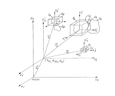
Fig. 4 represents a mapping of coin
sensor values in a three dimensional coordinate
system. The point f10, f20, A0at the intersection
of the Xl~ X2, X3 coordinate axes (~x coordinate
system~) represents the point of zero electrical
activity for the 6ensing circuits, while the point
fl0, f20, Ao represents an idle operating point for
the system. The point f10, f20, Ao is an arbitrary
starting point shown for exemplary purposes only
and can be changed in response to environmental
factors or the like. A vector C0 terminates at
this steady state idle operating point, and is
utilized to perform a mapping from the x
coordinate system, or the zero electrical activity
219~ill
system, to an x' coordinate system, the idle
sensor response coordinate system.
Thre regions R~, RB, and ~ represent
linear acceptance regions ~uch as ~hown in Fig. 3
for use in detecting genuine coins of three
differing denominations, while the regions CA~ C~
and Cc represent cluster regions for these same
three genuine coins. Regions S~ and SB are
examples of counterfeit coin cluster regions.
Vectors V1, V2 and V3, which ~riginate from the
origin of the x' coordinate system, terminate at
the genuine coin cluster centers for the sensor
response distributions for each of the coin
denominations, in effect mapping from the x'
system to x'' systems for each of the coin
clusters. This additional mapping to the x''
coordinate system saves on memory requirements and
computation time for the microprocessor.
Additional beneficial effects of this mapping
approach are discussed below.
Coin clusters are formed and optimized
for two sets of criteria. First, a mean vector
for each coin type, represented by vectors Vl, V2
and V3 in Fig. 4, is created. These vectors are
determined based on empirical statistical data for
each coin. Once these vectors are determined,
increased flexibility in acceptance criteria can
be accomplished by allowing and increasing
- ~tolerance~ for the location of each vector.
Typically, a tolerance of plus and minus one count
for each vector is needed to maintain acceptance
rates greater than 90%. The cluster center can
also be offset by a tolerance of plus or minus two
count permutations from its true position, and
aug~ented again to achieve a higher acceptance
rate of genuine coins.
219471 1
-18-
The second criteria is to minimize slug
acceptance. The goal of attaining the required
slug rejection rate is addressed by removing the
portion of the augmented coin cluster that
overlaps the cluster region of a slug or 61ugs.
An example of a portion that would be removed is
shaded portion O~ in Fig. 4. This portion OA has a
very low frequency of occurrence for valid coins,
and thus its removal minimally affects the coin
acceptance rate. In the presently preferred
embodiment, the resulting coin acceptance cluster
is represented by points in a three dimensional
space stored in a look-up table in memory.
Fig. 5 is a flow chart showing the
operation of this aspect of the invention. For an
initial coin denomination identification i=1
(block 503), the differences ( ~ ) between the
measured characteristics of the coins (X1...~)
(block 502) and the respective center point for
each vector (Cntr1,.... Cntr~) (block 504) are
compared against upper and lower limits (block
506). In terms of the variables used on Fig. 5, i
is the coin denomination index, m is the number of
measured coin parameters, (~1---~1) are the
lower limits and (U1~.. ..U~,) are the upper limits.
If the values do not fall within the
appropriate limits, then the coin denomination
index i is incremented (block 508) and the
values are compared against the limits for another
coin denomination. When the values are within
the limits, the ~ystem checks to see if the vector
formed by the values is in the look up table
(block 510); if the vector is in the table, then
the coin is accepted (block 512). The coin
denomination variable will be incremented until
valid data is determined or until all valid
denomination values have been ~earched (blocks
2~ 9~711
--19--
514, 516). Each time the coin denomination index
~i~ is incremented, the system looks to that
portion of the look-up table relating to that coin
denomination.
In this manner a specific level of coin
acceptance is achieved while maintaining a high
level of slug rejection. Further, the method and
apparatus of the present invention attains the
rejection of slugs that produce ~ensor responses
that are not distinguishable from those of genuine
coins following an approach as illustrated in Fig.
3.
A further advantage stems from the fact
that the points defining the clusters may be
represented as vectors whose components are all
integer numbers and the cluster volume is a finite
set of integer values. Sensor response
measurements are taken relative to the x'
coordinate system allowing the use of a smaller
set of numbers than if the measurements were taken
relative to the x coordinate system. In addition,
the V vectors map the x' coordinate system to the
x'' coordinate system. If the mean is again
removed from each measurement, then an even
smaller set of integer numbers is needed to
represent the cluster volume. Conseguently, a
canonical code may represent the cluster volumes.
Representation of the coin clusters by canonical
codes makes practical the use of low cost
microprocessors having limited memory ~pace, in
that the specific function for each cluster can be
easily stored in memory in a look-up table.
Further, a large degree of commonality
was found to exist between clusters of different
coin types relative to the x~ coordinate system.
This commonality permits the large common portion
of cluster information for all coins to be stored
~194711
-20-
only once, and the remaining coin specific values
to be stored separately in microprocessor memory.
Consequently, a savings in memory requirements is
realized.
In the preferred embodiment, the look-up
table is stored in memory in a sorted fashion in
order to permit a fast search through the table.
The search starts in the middle of the table, and
uses a search technigue for fast identification of
the portions of the table which contain the data
of interest.
It should be noted that in order to
stabilize the measurements and maintain a high
degree of genuine coin acceptance with varying
environmental changes, historical information for
each of the C0 and V vectors must be maintained,
and these vectors must also be varied when system
parameters change due to temperature, humidity,
component wear and the like. These vectors point
to the idle operating state of the system and are
functions of parameters which may experience step
changes as well as slow variations, all of which
reguire compensation and adaptive tracking to
provide a stable operating platform. Also, while
the V vectors for all coin types are compensated
in exactly the same manner, they can also be
compensated as a function of coin denomination.
It should ~lso be noted that the coin
acceptance cluster may be created in two
dimensions rather than three, based on measurement
of two coin characteristics rather than three.
ANTI-FRAUD AND ANTI-CHEAT
Another aspect of the present invention
involves an improved method and apparatus for
avoiding a fraud practice where slugs have been
used in a prior art coin validator in an attempt
219~711
-21-
to move the acceptance window toward the slug
distribution. The prior art method may be
understood by taking all f variables as
representing any function which ~ight be tested,
S such as frequency, amplitude and the like, for any
coin test. The specific discussion of the prior
art which follows will be in terms of frequency
testing for United States 5-cent coins using
circuitry as shown in Fig. 1 programmed to operate
as described below.
For initial calibration and tuning, a
number of acceptable coins, such as eight
acceptable 5-cent coins, are inserted to tune the
apparatus for 5 cent-coins. The frequency of the
output of sensor circuit 21 is repetitively
sampled and the frequency values f~.,ur.~ are
obtained. A maximum difference value, f, is
computed from the maximum difference between
f~,.ur~d and fO during passage of the first 5-cent
coin. f=max(f~ur~d - fO)-
Next, a dimensionless quantity, F, is
calculated by dividing the maximum difference
value f by fO where F=( f/fO). The computed F for
the first 5-cent coin is compared with the stored
acceptance limits to see if it lies within those
limits. Since the first 5-cent coin is an
acceptable 5-cent coin, its F value i6 within the
limits. The first 5-cent coin is accepted and
microprocessor 35 obtains a coin count C for that
coin.
The coin count C is incremented by one
every time an acceptable coin i6 encountered until
it reaches a predetermined threshold number.
Until that threshold number is reached, new F
values are stored based on the last coin Accepted.
When that threshold number is reached, a flag is
set in the 60ftware program to use the latest F
2194711
-22-
value as the center point to determine the
acceptance limits of the acceptance ~window~ for
subsequently inserted coins. The originally
stored limits are no longer used, and the new
limits may be based on the latest F value plus or
minus a constant, or computed from the latest F
value in any logical manner. Once t~e apparatus
is tuned as discussed above, it is capable of
performing in an actual operating environment.
The coin mechanism was designed to
continually recompute new F values and acceptance
limits as additional coins were inserted. If a
counterfeit coin was inserted, its F value
theoretically would not be within the acceptance
limits so the coin would be rejected. After
rejection of a counterfeit coin a new idling
frequency, f0, was measured and then the
microprocessor 35 awaited the next coin arrival.
Recomputation of the F values and
acceptance limits in this manner allowed the
system to self-tune and recalibrate itself and
thus to compensate for component drift,
temperature changes, other environmental shifts
and the like. In order for beneficial
compensation to be achieved, the computation of
new F values was done so that these values were
not overly weighted by previously accepted coins.
While achieving many benefits, the prior
art system has suffered because in practice a ~lug
exists whose measured characteristics overlap
those for a known acceptable coin as illustrated
in Fig. 7A. ~n Fig. 7A, the item designated 710
is a line distribution for certain measurement
criteria of a genuine coin. Curve 720 is a line
distribution for the same measurement criteria of
a slug. The overlap is shown as the shaded area
730 in Fig. 7A. As a result, the repeated
219~711
-23-
insertion of these slugs will move the window
center point toward the slug by tracking as those
slugs are accepted. Eventually, acceptance will
be 100~ for the slug and poor for the valid coin.
S The present invention addresses this
problem as discussed below.
Acceptance criteria for any given
denomination coin may be illustrated by the
~easured distribution of coin test dsta from the
center point of a coin acceptance window. In the
preferred embodiment of the present invention, as
discussed earlier in this application, the
dimensionless guantity F is computed and then
compared with stored acceptance limits to see if
the computed value of F for the coin being tested
lies within a certain di-stribution in the coin
acceptance window. Fig. 6 is a representation of
such a distribution having a center point at zero
and acceptance limits at ~+3~ and ~-3~. Item 610
in ~ig. 6 represents a measured criteria line
distribution for a genuine coin.
In practice, invalid coins have
distributions that slightly overlap those of
genuine coins. Item 710 in Fig. 7A depicts the
genuine coin line distribution of Fig. 6 having a
center point at ~0~, and the overlapping line
distribution of an invalid coin or slug having a
center point at ~5~. The invalid coin line
distribution is designated as 720. Of course,
there are distributions for invalid coins other
than that shown in Fig. 7A, includiny
distributions to the left of the genuine coin
distribution 710. The genuine coin distribution
and the invalid coin distribution shown in Figs. 6
and 7A are exemplary only.
It is readily seen that the line
distribution of characteristic data for the
-- 219~711
-24-
genuine coin overlaps with the line distribution
for the invalid coin in the shaded area 730 shown
in Fig. 7A. For a coin mechanism employing window
self-adjustment, such as that described above with
respect to the prior art, repeated insertion of
invalid coins, some of which have characteristics
just within the outer edges of the genuine coin
acceptance window, will cause the system to move
the center point of the coin acceptance window
toward the distribution pattern of the invalid
coin. This "tracking" eventually results in
acceptance of invalid coins and rejection of
genuine coins. A person wishing to cheat or
defraud the coin mechanism need only repeatedly
insert a certain invalid coin into the coin
mechanism, thereby in effect programming the
system to accept non-genuine coins, resulting in a
significant loss of revenue.
To combat such behavior, the present
invention provides for improved invalid coin
rejection by preventing this "tracking" of the
center point of the acceptance window toward the
invalid coin distribution. This is accomplished
by sensing any invalid coin that has parameters
which fall close to the outer limits of the coin
acceptance window, ~uch ~s within a "near miss"
area "z" in the invalid coin distribution between
points "3" and ~4" on the graph in Fig. 7A.
The ~equence of steps followed for this
method are set forth in the flow chart of Fig. 8.
First, a determination is made whether a submitted
coin i6 valid tblock 812, Fig. 8). Coins having
specified parameters within the genuine coin
acceptance window, for example as defined by
symmetrical limits J+3" and "-3" nround the center
point "0" of the genuine coin distribution of
Figs. 6 and 7A, ~re considered valid; thcse coins
219471~
-25-
outside of that coin acceptance window are
considered not valid.
If the coin is not valid, the system
determines whether the cheat mode flag i6 set
(block 802). If that flag is not set, a
determination is made whether the invalid coin
fits within the ~near miss~ area, ~z,~ between ~3~
and ~4~ on Fig. 7A (block 804). If the answer to
that inguiry is yes, the system moves the center
of the coin acceptance window a preset amount away
from the invalid coin distribution curve (block
806). For example, with reference to Fig. 7A, the
center of the coin acceptance window is moved from
~0~ to ~ . Alternatively, the right acceptance
boundary may be moved from ~3~ to ~2~. In either
case, very few genuine coins will not be accepted,
but essentially all invalid coins will now be
rejected, thereby preventing any attempted fraud.
A cheat counter is then cleared (block
808), and the cheat mode flag is set (block 810).
If another invalid coin is then inserted into the
mechanism, the system recognizes that the cheat
mode flag is set (block 802), ~nd no changes are
made to the center position of the coin acceptance
window.
With regard to the Fig. 7A example, the
center of the coin acceptance window is maintained
at its ~ position until a preset, threshold
number of ~alid coins of the s~me denomination are
counted in the cheat counter. The cheat counter
can be reset to zero if another invalid coin is
cubmitted to the mechanism which has a
characteristic which fits within the ~near mi~s~
area ~z~ on Fig. 7A.
Once the cheat counter reaches the
desired threshold number, the cheat mode flag is
cleared and the center of the coin acceptance
219~711
-26-
window is moved back to its original position.
These steps are shown on the Fig. 8 flowchart, in
the left-hand colu~n, blocks 812 to 824.
Specifically, after block 812 determines
that the coin is valid, block 814 recognizes that
the cheat mode flag is 6et. If the valid coin is
the same denomination as what triggered the cheat
mode flag (block 816), then the chea't counter is
incremented (block 818). When the cheat counter
reaches its preset threshold limit (block 820),
the cheat mode flag is cleared (block 822), and
the acceptance window is returned to its original
position (block 824).
In the Fig. 7A example, the center of the
coin acceptance window is moved from ~-lr back to
~on once the threshold number of valid coins is
counted in the cheat counter.
By this method, attempts to train the
coin mechanism to accept counterfeit coins, slugs
and the like are thwarted, in that the center of
the coin acceptance window will not move toward
the invalid coin distribution if the user
repeatedly inserts a number of the invalid coins
into the coin ~echanism, even though some of these
coins would normally be acceptable and some would
only miss being ~cceptable by a 6mall amount 6uch
that a slight movement of the acceptance criteria
would result in their acceptance. In fact,
according to this aspect of the present invention,
the coin acceptance window moves away from the
invalid coin distribution for certain non-valid
coins or slugs, until such time as a threshold
number of valid coins are counted.
The above described method can be used
for any denomination coins. Further, the value of
various parameter6 i6 adjustable, including but
not limited to the threshold value of genuine
2~ 94711
.
coins required to clear the cheat mode flag, the
width of that portion of the invalid coin
distribution which triggers the cheat mode (area
~z~ in ~ig. 7A), and the distance that the center
of the coin acceptance window i6 moved away from
the invalid coin distribution. These and other
parameters may be customized for each denomination
coin and any other special conditions relating to
the coin mechanism or the coins. ~or example, if
it is known that a counterfeit coin having a
certain distribution is often mistaken for a
genuine U.S. twenty-five cents coin, then the
acceptance window for this coin can be programmed
to move a distance out of the range of that
counterfeit coin and to stay there for a minimum
of lo or more genuine U.S. quarter coin
validations.
This anti-fraud and anti-cheat method and
apparatus may be used independently of the other
aspects of this invention in any coin testing
apparatus in which the coin criteria can be
adjusted by the control logic which controls the
coin, bill or other currency test apparatus.
However, the presently preferred embodiment is to
incorporate this anti-fraud, anti-cheat aspect in
conjunction with the other aspects of the present
invention in one system.
~MPROVED COIN hCCEPTANCE WINDOw CENTER SELF-
~DJUSTMENT
A method for self-adjustment of the
center of the
coin acceptance window involves accumulating a sum
of the deviations from the center of the coin
acceptance window for each coin. When the sum of
deviations equals or exceeds a pre-set value, the
- 219471 1
-28-
center position of the coin acceptance window is
adjusted.
By one aspect of the present invention,
only small or gradual deviations from the center
point of the coin acceptance window are added to
the running sum of deviations. Abrupt or large
deviations in the coin variables outside of this
small deviation band are ignored in terms of
center adjustment, as it is recognized that
adjustment based on such large deviations tends to
unduly shift the coin acceptance windows toward
the acceptance of counterfeit coins, slugs and the
like~ and away from acceptance of genuine coins.
~ig. 9 is a flow chart showing the steps
involved in this aspect of the present invention.
First, the coin mechanism is ~taught~ in the usual
manner, e.g., utilizing 8 valid coins to establish
the necessary information concerning the coin
acceptance window. Outside limits are then set
for the window in any one of a number of
conventional manners or using the cluster
technique described above. These steps are
combined in block 902, which states that the
window is established. If the coin is not
accepted as valid (block 904), no adjustment to
the center of the coin adjustment window
(designated in ~ig. 9 as CNTR) is made and the
system waits for the next coin (block 903).
If the coin is determined to be valid
(block 904), then the absolute value difference
between M, the measured criteria for that
particular coin, ~nd C~TR is compared to the
center adjustment deviation limit DEV (block 906).
If this absolute value difference is less than the
limit DEV, then the cumulative 5um value CS is
modified by adding to it the value ~CNTR - M~
(block 908).
219~711
-29-
If the absolute value difference between
M and CNTR exceeds the limit DEV (block 906), then
no adjustment is made to the cumulative sum CS,
and the system awaits arrival of the next coin.
When the cumulative sum CS equals or
exceeds a certain positive cumulative sum limit,
or is equal to or less than a negative cumulative
sum limit (block 910), the value of 'CNTR is
incremented by a preset amount or is decremented
by a preset amount, as appropriate (block 912).
The cumulative sum CS is then adjusted
accordingly, and the system awaits the arrival of
the next coin.
Thus, it is seen that only valid coins
having small deviations from the center value CNTR
of the coin adjustment window affect the self-
adjustment of that center value. Coins which
deviate outside this limited deviation range do
not effect the center self-adjustment. Since
counterfeit coins and slugs will almost in all
cases deviate from the center point CNTR more than
the limit DEV amount, this method virtually
insures that counterfeit coins, slugs and the like
will not affect the center self-adjust mechanism.
The method for protecting the center
self-adjustment mechanism described above allows a
wider coin acceptance window to be utilized,
thereby increasing the freguency that genuine
coins will be accepted by the system.
In the preferred embodiment, this
improved coin acceptance window center ~elf-
adjustment is utilized in combination with all
other aspects of the present invention. However,
it is to be understood that this center-adjust
method may be used independently of, or in various
combinations with, the aspects of the present
invention.
- - ' 219~71 1
-30-
RELATIVE VALUE COMPUTATION
It is beneficial to employ a low-cost
microprocessor to calculate the dimensionless F
value discussed above, which may also be referred
to as the relative value. To this end, in order
to perform calculations based upon the F value, a
scaling factor of 256 was utilized to ease
processing, and the resulting num~er was truncated
to the nearest integer.
This method of calculation resulted in
some loss of resolution. For example, when the
ratio of the scaling factor of 256 and the rest
value fO was greater than one, not all integer
values existed within the range covered by the
relative values F for a certain rest value f0. For
example, if the rest value f0 was 128 XHz, then the
relative value F would be even num~ers. (F= f/128
*256 = f* 2). Similarly, only odd values of F
existed if f0 was an odd number. Further, when the
rest value f0 changed, the list of non-existing
values changed also. Consequently, an expanded
look-up table was required in order to accomodate
all possible relative values F. This consumed
expensive memory space, and increased the
computation time spent for coin validation.
Also, use of such a high scaling factor
as 256 meant that oftentimes the integer value of
F was much greater than unity, and therefore extra
memory space was required to store the necessary
data for the F value, the center of the coin
acceptance window and the limits of that window.
~urther, for sensors operating at high
frequencies, validation resolution was lost, as
one integer relative value F represented several
possible actual shift values f, due to
truncation. For example, if a sensor operated at
- 219471 1
-31-
fD=1024 KHz, then 256 divided by 1024 equals 1/4,
which became the multiplier for the shift value
f. In this example, for f values of 4, 5, 6 and
7KHz, at fo=1024 RHz, ~=1 for all four f values.
This resulted in a loss in resolution which
reduced the ability of the coin mechanism to
separate counterfeit from genuine coins.
Lastly, in the prior art syste~s,
truncation of the calculation of the F relative
value resulted in a 0.5 bias of the center of the
coin adjustment window. This is because all
values between integers were truncated downward.
Since window centers could only be adjusted in
increments of plus or minus one, the center was
always biased by plus or minus 0.5 in steady
state. This further reduced the coin acceptance
rate. If a plus or minus one expansion of the
window width was used to compensate for the
reduced coin acceptance rate, the result was
increased acceptance of counterfeit coins.
Another aspect of the present invention,
described below, provides additional resolution
over the usage in the prior art systems of the 256
scaling factor. The relative value F is now
preferably calculated according to the following
equation:
F= f * E(fo)/fo, where E(fo) is the exponentially
weighted moving ~verage (also referred herein to
as the EWMA) of the rest value (f0) calculated for
each variable And coin denomination separately.
The theoretical equation for the exponentially
weighted moving average at coin increment is:
EQUATION A: E(fo)l ~ E(fo),l I W* (fOI - E(fo)ll) +
0.5 where W - weighing factor, And has a value
between O and 1. The result is rounded as opposed
to truncated to eliminate the 0.5 bias error. For
the first validation measurement, E(fo) is set to
219~711
equal fO where fO is the rest value during the
~teaching~ of the unit, as that teaching is
described earlier in this application. Through
computer simulation, it has been determined that a
value for W of 1/40 results in the best
performance of the coin mechanism. Over time, the
ratio of E(fo)JfDl approaches unity in the steady
state of fO.
The ratio of the exponentially weighted
moving average (E(fo)l) and the instantaneous rest
value (fOl) will have moderate deviations from
unity, with larger deviations being rare. On
those occasions when an abrupt change of the rest
value fO occurs, the ratio of E(fo)JfO may
significantly deviate from unity, partially
compensating for the shift value f change. This
makes it possible for window center self-
adjustment without a significant expansion of the
window. Further, while the window is being self-
adjusted the ratio of the E(fo)1/fol gradually comes
back to unity if no new perturbations occur for a
large enough amount of submitted coins.
Fig. 11 shows a step change of the rest
value fO to fO' and the curve of the exponentially
weighted moving average E(fo)l shown as a dotted
line. Any step changes in rest values, fO, that
would easily throw the shift values f outside the
acceptance window must be compensated for by E(fo)
to provide a smooth transition from one operating
point to another. Referring to Fig. 11, this
smooth transition chould be at a rate that is
slower than the tracking rate of the system.
E(fo)/fo allows the window center to track the
shift value with some delay as shown in Eig. 11.
As long as the relative deviation of the
rest value fO from its exponentially weighted
moving average, multiplied by the shift value f,
2194711
is within the range plus or minus 0.5, this aspect
of the present invention does not create gaps
between relative values F. This method provides
for a ~ufficient coin acceptance rate allowing for
fast self-adjustment of centers of coin acceptance
windows following abrupt and large changes in rest
values f0 in most cases. Further, the new method
produces relative values F having no loss of
resolution and al60 eliminates the 0.5 bias by
rounding, allowing for improved counterfeit coin
rejection. Another advantage is ease of
microprocessor implementation since the
exponentially weighted moving average can be
easily calculated. Current values of the
exponentially weighted moving average need to be
calculated separately for each rest value and
stored, and only one constant value of W need be
stored.
It should be noted that EQUATION A for
the exponentially weighted moving average given
above is just one example of an equation having
the required characteristics. The required
characteristics include that the ratio (E(fD)Jfo~)
must go to unity in steady state, and that during
a transition in rest the ratio (E(fo)/f~) must be
such that when multiplied by the shift value f,
the relative value F must fall within the
acceptance window, so that an adjustment of the
center of the coin acceptance window can be made.
The exponentially weighted moving average
(EWMA) can be calculated to compensate for various
changes such as unit aging, wear, contamination
and cleaning, ambient temperature, etc. This can
be accomplished in the following manner, as shown
in the flow chart of Fig. 10.
The initial EWMA (E(fo)) eguals the rest
value f~ at the time the mechanism is ~taught~.
2194711
-34-
Deviations between the subseguently computed EWMA
and the relevant rest value fO~ are then summed
(block 102, Fig. 10). When the absolute value of
the sum of deviations (S1) exceeds a threshold
value l/W (block 104), then the EWMA is
incremented or decremented by a preset amount
(depending on the sign of the deviation sum), and
the deviation sum is adjusted accordingly (block
106). In the preferred embodiment, the EWNA is
moved ~+1~ or ~ when the sum of deviations
exceeds the threshold value of l/U. If the sum of
deviations does not exceed the threshold, the
system awaits arrival of the next coin (block
112).
In place of frequency, any parameter
having a rest value (such as amplitude) may be
used.
A further aspect of the present invention
involves combining all of the above disclosed
methods in one coin, bill or other currency
validation apparatus. Of course, other
combinations and permutations of the above aspects
are also contemplated and may be found beneficial
by those skilled in the art.
In the preferred embodiment, with regard
to certain aspects of the present invention, the
microprocessor 35 is programmed according to the
attached printout appended hereto as an Appendix;
however, the operation of the electronic coin
testing apparatus 10 and the methods described
herein, will be clear to one skilled in the art
from the above discussion.