Note: Descriptions are shown in the official language in which they were submitted.
CA 02194742 1999-07-16
Process and Device for Coating a Substrate Surface
The invention relates to a process for coating a substrate surface with a
layer of
inorganic material, which is vaporized in a vacuum chamber evacuated to at
least 10-3
mbar by bombarding with an electron beam from a high voltage electron-beam gun
and deposited on the substrate surface. Within the scope of the invention is
also a
device for performing and applying the process.
Problems of electrostatic charging arise while electron-beam coating substrate
materials that do not conduct electricity. These problems are due to the fact
that the
electrons from the electron-beam gun are not conducted off in a definite
manner, this
because the electrostatic charging cannot be led off the electrically
insulating coating
and substrate materials nor from the coated walls of the vacuum chamber which
also
become insulating aftc,r a certain time.
The charging phenomena express themselves e.g. in non-uniform focusing of the
electron-beam, in no:n-defined alignment of the beam as a result of non-
defined
electrostatic fields and in charging of the substrate material which,
especially when
coil coating plastic films, can lead to considerable coiling problems. The
electrostatic
charge can also lead to pinholes in the film as a result of discharging. The
build up of
the electrostatic charge can also lead to overlapping of the film.
Known from the European patent document EP-A-0545863 is a process of the kind
mentioned at the start, in which a low energy, ionizing electron-beam forming
a
plasma is passed through the gas phase of inorganic material to an anode. The
resultant gas discharging leads to removal of the electrostatic charge. The
disadvantage of this nnentioned method is that a second electron-beam gun bas
to be
housed in the vacuum chamber.
In view of these facts, the present invention seeks to provide a process of
the type
described at the start, in which the undesired electrostatic charging inside
the vacuum
chamber can be prevented effectively using simple means.
CA 02194742 1999-07-16
- la-
In accordance with tlhe invention gas discharging is created between the point
of
incidence of the electron beam on the inorganic material to be vaporized and
an anode
such that the electrostatic charge created by the high voltage electron-beam
gun flows
off via the anode.
In accordance with one aspect of the invention there is provided a process for
coating,
which comprises: providing a substrate surface and an anode spaced therefrom
in a
vacuum chamber with gas therein; coating said substrate surface with a layer
of
inorganic material by vaporizing said inorganic material in said vacuum
chamber
evacuated to 10-3 mbar or less, including bombarding said inorganic material
with an
electron beam from an electron-beam gun to vaporize said inorganic material,
and
wherein said gun creates an electrostatic charge, and wherein there is a point
of
incidence (A) between the inorganic material and the electron beam, and
depositing
the vaporized inorganic material on the substrate surface as a coating;
wherein gas
discharge is created in the gas and in the vaporized inorganic material
between the
point of incidence (A) of the electron beam on the inorganic material to be
vaporized
and said anode such that the electrostatic charge created by the electron-beam
gun
flows off via the anode; with said anode having an electrical conductivity and
a
surface, and wherein, in order to maintain the electrical conductivity at the
surface of
the anode and to prevent the anode from being coated, the anode is heated to a
temperature exceeding; that at which the vaporized inorganic material
condenses; with
the voltage applied to said electron-beam gun being at least 5 kV and wherein
the
substrate is a non-electrically conductive substrate and said coating is a non-
electrically conductive; material.
CA 02194742 1999-07-16
- 1 b-
In accordance with another aspect of the invention there is provided a device
for
coating, which comprises: a substrate surface; an anode spaced from the
substrate
surface; a vacuum chamber evacuated to at least 10-3 mbar; a layer of
inorganic
material in said chamber; a high voltage electron-beam gun for emitting an
electron
beam to bombard said inorganic material and vaporize said inorganic material
and
deposit the vaporized inorganic material on the substrate surface, wherein gas
discharge is created between the point of incidence (A) of the electron beam
on the
inorganic material to be vaporized and said anode such that the electrostatic
charge
created by the high voltage electron-beam gun flows off via the anode.
2194742
-2-
In order to maintain the electrical conductivity at the surface of the anode,
this is preferably
heated to a temperature exceeding that at which the vaporised inorganic
material condenses.
To that end the anode is usefully heated electrically by way of a transformer
polarised to
couple the heating current into the electrical circuit.
Under optimal process parameter settings, a current equivalent to the emission
current of the
electron-beam gun flows through the anode voltage supply. This means that the
whole of the
electrostatic charge created by the electron-beam gun flows off over the
anode.
The pressure of gas can vary ,in particular in the course of extended coating
cycles, to such
an extent that the full amount of emission current does not flow off via the
anode. It can,
therefore, prove advantageous to keep the pressure in the vacuum chamber
constant by
varying the inlet of gas, in order to stabilise the gas discharging.
Regulation is achieved
preferably automatically via closed cycle control by means of which the gas
pressure is
I 5 normally set at a value of 10'3 to 2. 10'~ mbar.
A device suitable for performing the process according to the invention is
such that the anode
in the region of the inorganic material to be vaporised is preferably situated
outwith the direct
vaporisation zone.
The inorganic material to be vaporised is normally prepared in a crucible, may
however, also
be situated e.g. on a water cooled plate.
As the anode is exposed to high temperatures, it must be made of a suitably
temperature
resistant material. The anode is therefore preferably of tungsten, tantalum,
molybdenum or
graphite in the form of wire, rod, tube, mesh or net.
The process according to the invention is suitable in particular for coating
plastic films for the
packaging industry and in general for coating non-electrically conductive
substrate materials
with non electrically conductive layers starting from non electrically
conductive coating
materials.
Further advantages, features and details of the invention are revealed in the
following
description of preferred exemplified embodiments of the invention and with the
aid of the
schematic drawing:
case 2087
X194742
-3-
Fig. I a sketch showing the principle of an arrangement for coating purposes;
Fig. 2 a sketch showing the principle of an arrangement for coating coils of
film
material;
Fig. 3 cross-section through a coated laminate film.
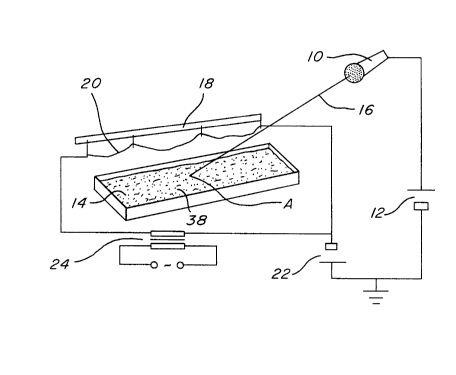
Figure I shows a high voltage electron-beam gun 10 connected to a direct
current high
voltage supply 12. The electron beam 16 emitted from the electron-beam gun 10
is directed
onto a water-cooled plate 14 bearing the inorganic material 38 to be vaporised
and its point
of contact A with the plate 14 is scanned over the plate surface i.e. the
electron beam travels,
program controlled, over the surface of the inorganic material that is to be
vaporised. In that
process the inorganic material is heated by the energy of the impinging
electron beam 16 and
vaporises.
An anode 20 - for example in the form of a tungsten filament - is arranged,
likewise in a
water-cooled holder 18, in the region of the plate 14 with the material 38 to
be vaporised.
The anode 20 is connected to a direct current anode voltage supply unit 22.
The coupling of
the anode heating current takes place via a transformer 24.
In the version according to figure 2 a plastic film 28 is uncoiled from a
first roll 30 and pulled
over a roll 34. The plastic film 28 lying on the roll 34 serving as a
substrate support forms the
substrate surface 3 S in the working area. After the coating has been
performed, the plastic
film 28 is coiled onto another roll 32. For reasons of clarity, any deflection
rolls have been
omitted in the drawing.
The inorganic material 38 is heated by the electron beam 16 emitted by the
electron-beam
gun 10 forming a gas phase 40 of inorganic material 3 8.
Between the point of contact A where the electron beam 16 strikes the
inorganic material in
the crucible 36 and the heated anode wire 20 and under suitably chosen process
parameters
gas discharging occurs in the gas which is fed to the vacuum chamber in
metered amounts via
a gas inlet system which is not shown in the drawing and in the gas phase 40
of inorganic
material 3 8.
The anode 20 itself is prevented from being coated by heating the anode to a
temperature
above that at which the vaporised inorganic material 38 condenses.
case 2087
2194~~2
-4-
This way the gas discharging can be maintained throughout the whole process.
The
electrostatic charging introduced by the electron-beam gun 10 flows to earth
via the gas
discharging with the result that a stable closed circuit of current is
produced and an electric
charge can no longer build up at sites where this is undesired. Furthermore,
the coating
material no longer becomes electrostatically charged; consequently there can
be no
defocusing of the beam.
As already mentioned, on selecting suitable process parameters a current
equivalent to the
emission current of the electron-beam gun 10 flows through the direct current
anode voltage
supply unit 22.
All inert gases, especially noble gases, preferably argon are suitable for non-
reactive coating
processes. If a reactive vapour coating process is to be performed, then the
gas required for
discharging may of course also be the reactive gas in question, or if desired
combined with an
inert gas.
For reasons of clarity, all auxiliary equipment and devices for heating the
cathode of the
electron-beam gun 10 have been omitted in figures 1 and .2. Likewise, not
shown in the
drawing is a controllable gas feeding system with gas distribution system near
the organic
material to be vaporised, nor a system for measuring pressure.
Suitable inorganic materials for vaporisation are in principle all known
materials which, after
precipitating from the gas phase, with or without chemical reaction, form a
layer that serves
as a barrier for gas and moisture. Examples thereof are silicon monoxide,
silicon dioxide
titanium oxide, zirconium oxide, aluminium oxide and magnesium oxide. These
oxides may
be mixed or doped. Further, these metals may be vaporised and, during the
coating process,
at least one reactive gas e.g. oxygen, nitrogen, hydrogen and/or acetylene
introduced, with
the result that the corresponding oxides, nitrides, carbides or mixed
components are formed.
Of course, reactive gases may also be added if the material to be vaporised is
already present
as oxide, nitride and/or carbide.
The voltage applied to the high voltage electron-beam gun is preferably at
least 5 kV,
especially at least 10 kV, at a current of some amperes. The high voltage
electron-beam gun
operates e.g. with an energy of 35 kW.
Using the process according to the invention deposition rates of at least 0.01
pm/sec are
achieved, advantageously however in the region of 0.5 to 1 pm/sec.
case 2087
219742
The substrate surfaces to be coated by the process according to the invention,
especially in
the case of plastic films, are advantageously, moved during the coating stage.
The rate of
throughput of the plastic films usefully lies in the region of 1 to 10 m/sec,
especially 3 to 6
m/sec. The plastic films are e.g. of polyester (PET), polyethylene (PE) or
polyamide (PA).
The coated laminate film shown in figure 3 comprises a plastic film base 28,
an inorganic
layer 42 vapour deposited to provide a barrier to permeation and a sealable
film 44 which has
been applied after the vapour deposition process.
Ezample
Plastic films with vapour deposited SiOY are employed today for producing
transparent films
with good barriers to permeation of gas and water vapour. The coating with
SiOY is
performed at high coating rates, usefully by means of electron beams. This
process can be
1 S accelerated and stabilised by means of the process according to the
invention with no
electrostatic charging phenomena such as pinholes due to discharging or
overlapping of the
film due to electrostatic charging.
The width being coated is e.g. 700 mm. The polyester film to be coated is 12
p,m thick. The
crucible filled with Si0 granules is e.g. 840 mm long. The anode is an e.g. 1
mm thick
tungsten wire, which is situated, insulated, above the crucible slightly
outwith the immediate
zone where vaporisation occurs. Likewise in the region of the crucible is a
gas distribution
pipe through which the gas is introduced and fed to the gas discharging zone
via thin
openings. The gas, argon for example, is fed to the vacuum chamber in a
controlled manner
regulated by pressure, and is kept at a constant pressure of e.g. 5 x 10~
mbar. The direct
current anode voltage supply operates at a voltage of 250 V, and the heating
of the tungsten
wire anode is effected by a 50 Hz alternating current of 30 A. The
accelerating voltage of the
electron-beam gun is 35 kV, the emission current of the gun is 1.2 A. This
current, however,
also flows over the tungsten wire of the anode. Under the conditions set by
the chosen
parameters the thickness of the layer deposited on the film is 50 nm at a
coating rate of 600
m/min, which is adequate to achieve a good barner layer. This rate of
vaporisation is at least
twice as high as the vaporisation rate achieved by conventional coating units
operating under
conditions that do not lead to pronounced damage of the substrate film. The
film can be
coiled without the slightest problem of discharging. Also, there is no
electrostatic discharging
through the film.
case 2087