Note: Descriptions are shown in the official language in which they were submitted.
21 94837
-
LABEL WITH A METALLIC LAYER OF CONTROLLED THICKNESS
FIELD OF THE INVENTION
The present invention relates to a novel label characterized by a
metallic layer of controlled thickness. More particularly, the present
invention relates to a label cont~ining a thin metal layer and showing
transparency and reflect*ity.
PRIOR ART OF THE INVENTION
As one of decorative processes of molded plastic articles, the so
called met~ ing process by which a thin layer of a metal is formed on a
molded plastic article has heretofore been known. As the met~li7.ing
process, for example, the chemical-electric plating process, the vacuum
vapor deposition process, the sputtering process, the ion p~ating process,
the hot stamping process, coating of mixed metal powder, and mi~ing of
metal powder into a material for molding are used. Plastic films coated
with a metal layer on the surface by a PVD process (a physical vapor
deposition process), such as the vacuum vapor deposition, the sputtering
process, and the ion plating process, are used in many applications,
such as labels, tapes, gold and silver threads, and films for light
shielding or heat insulation. Particularly, films having good gloss, such
as rigid polyvinyl chloride films, acetate films, and polyester films of a
larger thickness, are coated with aluminum and used for labels and
stickers.
However, when a film having a metal layer formed by vapor
- 2 ! 94~37
deposition on the surface is used for a label, the label has drawbacks in
that the label is not always satisfactory in view of artistic design because
the metal layer formed by vapor deposition is opaque, and that
observation of the content of a container is difficult when it is attached to
a transparent container.
SUMMARY OF THE INVENTION
The present invention accordingly has an object to provide a label
with a metallic layer of controlled thickness which provides remarkably
beautiful appearance when the film is printed, is suitable for artistic
design because it is transparent even though it shows metallic gloss, and
allows easy observation of the content of a container when the film is
used as a label on a transparent container.
As the result of extensive investigations undertaken by the present
inventors to develop a label with a metallic layer of controlled thickness
having the advantageous properties described above, it was discovered
that the object can be achieved by a film comprising a transparent or
semi-transparent film, a metallic layer which is formed by vapor
deposition, has a specific light transmittance, and is ls~min~ted on one
side of the film, and a layer of an adhesive material l~min~ted on the
metallic layer, or by a film comprising a transparent or semi-
transparent film, a metallic layer which is formed by vapor deposition,
has a specific light transmittance, and is l~min?~ted on one side of the
film, a protective layer l~min~ted on the metallic layer, and a layer of an
adhesive material ls,min~ted on the other side of the film. The present
21 94837
invention has been completed on the basis of the discovery.
Thus, the present invention provides:
(1) A label with a metallic layer of controlled thickness comprising a
transparent or semi-transparent film, a metallic layer which is formed
by metal deposition, has a light transmittance of 3 to 70 %, and is formed
on one side of the film, and a layer of an adhesive material formed on the
metallic layer (referred to as label I with a metallic layer of controlled
thickness hereinafter); and
(2) A label with a metallic layer of controlled thickness comprising a
transparent or semi-transparent film, a metallic layer which is formed
by metal deposition, has a light transmittance of 3 to 70 %, and is formed
on one side of the film, a protective layer formed on the metallic layer,
and a layer of an adhesive material formed on the other side of the film
(referred to as label II with a metallic layer of controlied thickness
hereinafter).
The preferred embodiments of the present invention include:
(3) The label with a metallic layer of controlled thickness described in (1),
wherein the label additionally comprises a layer of printing in between
the transparent or semi-transparent film and the metallic layer, or on
the side of the film opposite to the side on which the metallic layer is
deposited;
(4) The label with a metallic layer of controlled thickness described in (3),
wherein the label additionally comprises a protective layer for printing
which is formed on the layer of printing;
(5) The label with a metallic layer of controlled thickness described in (2),
21 94837
wherein the label additionally comprises a layer of printing formed on
the protective layer for metal;
(6) The label with a metallic layer of controlled thickness described in (5),
wherein the label additionally comprises a protective layer for printing
formed on the layer of printing;
(7) The label with a metallic layer of controlled thickness described in
any of (1) to (6), wherein the transparent or semi-transparent film is
treated with corona discharge or has an under coat on one or both sides
thereof; and
(8) The label with a metallic layer of controlled thickness described in
any of (1) to (7), wherein the metallic layer formed by metal deposition is
an aluminum layer.
(9) The label with a metallic layer of controlled thickness described in
any of (1) to (8), wherein the label additionally comprises a release liner
l~min~ted on the layer of an adhesive material;
BRIEF DESCRIPTION OF THE DRAWINGS
Figure 1 exhibits a section view showing the construction of an
example of the label with a metallic layer of controlled thickness of the
present invention.
Figure 2 exhibits a section view showing the construction of
another example of the label with a metallic layer of controlled thickness
of the present invention.
The numbers and characters in the figures have the n~e~nings as
listed in the following:
- 21 q4Q~37
a substrate film
2 an under treatment layer
3 a metallic layer formed by metal deposition
4 a protective layer
5 a layer of an adhesive material
6 a release liner
7 an ink receiving layer
8 a layer of printing
9 a protective layer for printing
10 a protective layer
DETAILED DESCRIPTION OF THE INVENTION
In the label with a metallic layer of controlled thickness of the
present invention, the transparent or semi-transparent film used as the
substrate film is not particularly limited. A suitable film for the
substrate film can be selected from various types of film, such as
cellulose triacetate, cellulose diacetate, cellophane, oriented
polypropylene, cast poly~,o~ylene, low density polyethylene, polystyrene,
polycarbonate, polyvinyl alcohol, polyvinyl chloride, and polyethylene
terephthalate. The thickness of the substrate film is generally in the
range of 12 to 100 ~lm. The substrate film may be colored.
In the present invention, for the purpose of increasing adhesion of
the substrate film with a metallic layer formed by metal deposition, a
layer of printing, a layer of an adhesive material, and other l~min~ted
layers, an under treatment layer may be formed on one or both sides of
-- 21 94837
the substrate film by a surface treatment to increase the surface energy,
to polarize the surface, or to increase the affinity of the surface.
Examples of the process for forming the under treatment layer include
(1) a process of oxidation of the surface, (2) a process of forming
roughness on the surface, and (3) a process of forming an under coat.
Examples of (1) the process of oxidation of the surface include
treatment with corona discharge, treatment with chromic acid (a wet
process), treatment with flame, treatment with hot air, exposure to
ozone, and irradiation with ultraviolet light. F~ mples of (2) the process
of forming roughness on the surface include sand blasting and
treatment with a solvent. The process for forming the under treatment
layer can be suitably selected in accordance with the type of the substrate
film. In general, the treatment with corona discharge is preferably used
because of superior effect and easier operation.
The treatment with corona discharge is the process most widely
used for surface treatment of plastic films. This process is, for example,
conducted as described in the following. An electrode connected to an
apparatus for generating a high voltage and a metal roll covered with a
polyester film, a hypalon film, or an EP rubber are disposed at a distance
of 0.5 to 0.6 mm to each other. High voltage corona is generated at the
gap between the electrode and the metal roll by application of a high
voltage of thousands volts to tens of thousands volts with a high
frequency of hundreds kilocycles per second. When a substrate film
passes through the gap at a constant speed, carbonyl groups and the like
are formed on the surface of the substrate film by the reaction with ozone
- 21 94837
.
and nitrogen oxides formed by the corona discharge, and the surface of
the substrate film is made hydrophilic. The degree of the treatment can
be adjusted by the distance of the gap, the voltage, the consumed
electricity, the thickness of the material covering the metal roll, and the
speed of the substrate film passing through the gap. As the apparatus
used for the treatment with corona discharge, an apparatus using an
electrode movable to a specified direction in combination with a fixed
electrode, an apparatus which treats both sides of a substrate film with
corona ~iisch~rge, or an apparatus which prevents formation of the area
not treated with corona discharge by adjusting arrangement of the
electrodes, may be used in place of the apparatus having the fixed
electrodes.
As (3) the process of forming an under coat, a process in which the
surface is coated with an acrylic resin, a polyester resin, a polyurethane
resin, or a vinyl acetate resin is generally used. The thickness of the
under coat layer is generally about 0.1 to 10 ~lm. The under coat layer
may be colored.
The label I with a metallic layer of controlled thickness of the
present invention has the construction comprising a metallic layer
which is formed by metal deposition, has a light transmittance of 3 to 70
~o on the substrate film, and a layer of an adhesive material l~min~ted
on the metallic layer, as the essential constituting layers thereof.
The metallic material forming the metallic layer by metal
deposition is not particularly limited as long as the material can be used
for metal deposition by the PVD process. Examples of the metallic
21 94837
material include metals, such as aluminum, chromium, nickel,
titanium, copper, gold, and silver; alloys of metals; and compounds of
metals. Among these metallic materials, aluminum is particularly
preferable because of superior balance of easiness for metal deposition,
economic advantage, and adaptability for artistic design.
Preferable examples of the process for metal deposition include
various types of the PVD process, such as the vacuum vapor deposition
process, the sputtering process, and the ion plating process. In the
vacuum vapor deposition process, for example, a metallic material for
forming a layer by metal deposition and a substrate film are placed
under a high vacuum. The metallic material is vaporized by heating
and attached to the surface of the substrate film by condensation to form
a thin layer of the metallic material. In the sputtering process, for
example, argon gas of a low pressure is introduced into a chamber of a
high vacuum. A metallic material used for forming the metallic layer is
placed at the cathode, and glow discharge is generated. The argon ions
formed by the glow discharge sputter the metallic material to cause
scattering of the metallic material. The scattered metallic material is
attached to and accumulated on the surface of the substrate film to form
a layer of the metallic material. In the ion plating process, for example,
a substrate film is placed on the cathode and a metallic material used for
vaporization is placed on the anode. Particles of the vaporized metallic
material are ionized while the particles pass through glow discharge.
The ionized particles of the metallic material are strongly adsorbed on
the surface of the substrate film to form a layer of the metallic material
21 94837
with enhanced adhesion.
In the present invention, it is necessary that the light
transmittance of the metallic layer formed by metal deposition be in the
range of 3 to 70 %. When the light transmittance is less than 3 %, the
obtained label is inferior in transparency, and the advantageous property
for artistic design cannot be obtained. Moreover, observation of the
content becomes difficult when the label is used for a transparent
container. When the light transmittance is more than 70 %, it is difficult
that the desired metallic gloss is obtained, and the object of the present
invention cannot be achieved. The light transmittance of the metallic
layer formed by vapor deposition is particularly preferably in the range of
10 to 60 %.
The light transmittance can be controlled by the thickness of the
metallic layer formed by metal deposition. The preferable thickness of
the metallic layer is different in accordance with the type of the metal
constituting the metallic layer and cannot be specified. The thickness is
generally selected in the range of 10 to 200 ~.
The light transmittance described above are measured in
accordance with the method of Japanese Industrial Standard K 7105.
The label of the present invention has metallic gloss. The light
reflection of the metallic gloss is preferably in the range of 20 to 80 %,
more preferably in the range of 30 to 70 %. When the light reflection is
less than 20 %, the gloss may be inferior. When the light reflection is
more than 80 %, the transparency may be inferior. The light reflection is
measured in accordance with the method of Japanese Industrial
~ 21 94837
Standard K 7105.
In label I with a metallic layer of controlled thickness of the
present invention, a layer of an adhesive material is formed on the
metallic layer formed by metal deposition. A protective layer may be
formed in advance on the metallic layer before the layer of an adhesive
material is formed on the metallic layer to protect the metallic layer and
to promote the adhesion between the metallic layer and the layer of an
adhesive material. For the protective layer, an acrylic resin, a polyester
resin, a polyurethane resin, or a vinyl acetate resin is generally used.
The thickness of the protective layer is generally about 0.1 to 10 llm.
The type of the adhesive material used for the layer of an adhesive
material is not particularly limited. Any of adhesive materials
conventionally used for lables, for example, glues such as vinyl acetate or
starch, thermal sensitive adhesives and pressure sensitive adhesives,
can be used. The thickness of the layer of an adhesive material is
generally in the range of 4 to 50 ,um.
In label I with a metallic layer of controlled thickness of the
present invention, a layer of printing is generally formed. The layer of
printing may be formed on the side of the substrate film opposite to the
side on which the metallic layer is formed. The layer of printing may
also be formed between the substrate film and the metallic layer. As the
ink used for forming the layer of printing, an ink cont~ining a binder,
such as an acrylic resin, a polyester resin, a polyurethane resin, a
polyvinyl chloride resin, a vinyl chloride-vinyl acetate copolymer resin, a
butyral resin, a nitrocellulose resin, an acetylcellulose resin, and a
21 ~4837
polystyrene resin; coloring agents, such as pigments and dyestuffs;
extender pigments; and solvents; is used. The layer of printing can be
formed by using the ink described above in accordance with a
conventional printing process, such as the gravure printing process, the
screen printing process, the offset printing method, and the flexo
printing process.
When the layer of printing is formed on the side of the substrate
film opposite to the side on which the metallic layer is formed, the
substrate film may be treated on the surface as described above in
advance and coated with an ink receiving layer on the treated surface,
and the layer of printing may be formed on the ink receiving layer to
improve the property for printing. The thickness of the ink receiving
layer is generally in the range of 0.1 to 10 ~lm. The ink receiving layer
may be colored.
In label I with a metallic layer of controlled thickness of the
present invention, when the layer of printing is formed on the side of the
substrate opposite to the side on which the metallic layer is formed, a
protective layer for printing may be formed on the layer of printing.
Examples of the protective layer for printing include a layer of an acrylic
resin, a layer of a polyurethane resin, and a layer of a resin of an
ultraviolet curing type. The thickness of the protective layer for printing
is generally in the range of 0.1 to 10 ~lm.
In label I with a metallic layer of controlled thickness of the
present invention, a hard coat layer or a layer to prevent reflection may
also be formed on the side of the substrate film opposite to the side on
21 94837
which the metallic layer is formed.
In label I with a metallic layer of controlled thickness of the
present invention, a release liner may be attached to the layer of an
adhesive material. Examples of the release liner include materials
prepared by coating a releasing agent, such as a silicone resin, on
various types of paper, such as glassine paper, coated paper,
polyethylene, l~minated paper, or on various types of film.
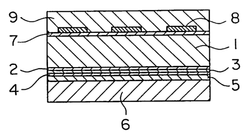
Figure 1 exhibits a section view showing the construction of an
example of label I with a metallic layer of controlled thickness of the
present invention. In this construction, an under treatment layer 2, a
metallic layer formed by metal deposition 3, a protective layer 4, a layer of
an adhesive material 5, and a release liner 6 are formed successively on
one side of the substrate film 1. On the other side of the substrate film 1,
an ink receiving layer 7, a layer of printing 8, and a protective layer for
printing 9 are formed successively.
A layer of printing may be formed bewteen the layer of an adhesive
material 5 and the protective layer 4.
Label II with a metallic layer of controlled thickness of the present
invention is described in the following.
Label II with a metallic layer of controlled thickness of the present
invention has the construction comprising a metallic layer which is
formed by metal deposition, has a light transmittance of 3 to 70 ~o, and is
formed on one side of the film, a protect*e layer formed on the metallic
layer, and a layer of an adhesive material coated on the other side of the
substrate film, as the essential constituting layers thereof.
21 94837
The metallic material and the process used for forming the
metallic layer are the same as those used in label I with a metallic layer
of controlled thickness described above. Before the metallic layer is
formed by metal deposition, an under coat layer may also be formed on
the substrate film in advance in the same manner as that in label I with
a metallic layer of controlled thickness.
In label II with a metallic layer of controlled thickness, a
protective layer is formed on the metallic layer to protect the metallic
layer. For the protective layer, an acrylic resin, a polyester resin, a
polyurethane resin, or a vinyl acetate resin is generally used. The
thickness of the protective layer is generally about 0.1 to 10 llm. The
protective layer may be colored.
In label II with a metallic layer of controlled thickness, a layer of
an adhesive material is formed on the side of the substrate opposite to the
side on which the metallic layer is formed. The type and the thickness of
the layer of an adhesive material are the same as those of the layer of an
adhesive material in label I with a metallic layer of controlled thickness.
In label II with a metallic layer of controlled thickness of the
present invention, a layer of printing is generally formed. The layer of
printing is preferably formed on the protective layer described above. The
ink used for the layer of printing, the process for forming the layer of
printing, and the thickness of the layer of printing are the same as those
of the layer of printing in label I with a metallic layer of controlled
thickness described above. A protective layer for printing may also be
formed on the layer of printing in the same manner as that in label I
21 94837
-
with a metallic layer of controlled thickness.
In label II with a metallic layer of controlled thickness, a release
liner may also be attached to the layer of an adhesive material in the
same manner as that in label I with a metallic layer of controlled
thickness.
Figure 2 exhibits a section view showing the construction of an
example of label II with a metallic layer of controlled thickness of the
present invention. In this construction, an under treatment layer 2, a
metallic layer formed by metal deposition 3, a protective layer 10, a layer
of printing 8, and a protective layer for printing 9 are formed successively
on one side of a transparent or semi-transparent substrate film 1. On the
other side of the substrate film 1, a layer of an adhesive material 5 and a
release liner 6 are formed successively.
A layer of printing may be formed between the substrate film 1 and
the layer of an adhesive material 5.
To sllmmArize the advantages of the present invention, the label
with a metallic layer of controlled thickness of the present invention
provides remarkably beautiful appearance when the film is printed, is
suitable for artistic design because it is transparent even though it shows
metallic gloss, and allows easy observation of the content of a container
when the film is used as a label on a transparent container. Thus, the
label of the present invention has a very high commercial value.
The present invention is described more specifically with reference
to examples in the following.
21 94837
Example 1
A polyester film of 38 ~lm thickness was treated with corona
discharge on one side. Then, aluminum was deposited on the treated
surface by using an apparatus for vacuum vapor deposition (a product of
Leybold Company; High Vacuum Web Coater) (light transmittance, 60
%; light reflection, 25 ~o).
The side of the film opposite to the side on which aluminum was
l~min~ted was coated with a polyester resin (a product of Toyobo Co.,
Ltd.; trade name, Vylon RV200) to the thickness of 0.2 ~lm (dry) to form
an ink receiving layer.
The aluminum layer formed by the metal deposition in the above
was coated with a polyester resin (a product of Toyobo Co., Ltd.; trade
name, Vylon RV280) in an amount of 0.2 g/m2 (dry) to form a protect*e
layer. The formed protective layer was coated with an acrylic adhesive
material (a product of Toyo Ink MFG. Co., Ltd.; trade name, Oribine
BPS-5127) to a thickness of 15 llm (dry), and a release liner (a product of
Lintec Co., Ltd.; trade name, 8K) was attached to the adhesive layer thus
formed.
Printing was made on the ink receiving layer by an offset printer to
prepare a label. When this label was attached to a glass bottle, the label
was shown to be a novel label having beautiful metallic gloss through
which the content of the glass bottle could be observed.
F,x~mple 2
A biaxially oriented polypropylene film of 50 ,um thickness was
- 21 94837
treated with corona discharge on one side. The treated surface was
coated with a polyester resin (a product of Toyobo Co., Ltd.; trade name,
Vylon RV200) to a thickness of 0.3 llm (dry) to form an ink receiving
layer.
The coated film was treated with corona discharge on the side
opposite to the side on which the ink receiving layer was formed. Then,
aluminum was laminated on the treated surface by metal deposition by
using the apparatus for vacuum vapor deposition (light transmittance,
20 %; light reflection, 55 ~o).
The aluminum layer formed in the above was coated with the
acrylic adhesive material to a thickness of 15 ,um (dry), and a release
liner was attached to the adhesive layer thus formed.
Printing was made on the ink receiving layer by an offset printer to
prepare a label. When this label was attached to a glass bottle, the label
was shown to be a novel label having beautiful metallic gloss through
which the content of the glass bottle could be observed.
F~x~mple 3
A bi~xi~qlly oriented polypropylene film of 50 llm thickness was
treated with corona discharge on one side. The treated surface of the
film was coated with a polyester resin (a product of Toyobo Co., Ltd.;
trade name, Vylon RV-290) to a thickness of 0.2 llm (dry) to form an
under treatment layer. Then, aluminum was laminated on the formed
under treatment layer by metal deposition by using the apparatus for
vacuum vapor deposition (light transmittance, 10 %; light reflection, 65
16
2 1 94837
%) .
The aluminum layer formed by metal deposition in the above was
coated with a polyester resin (a product of Toyobo Co., Ltd.; trade name,
Vylon RV200) to a thickness of 0.3 ~lm (dry) to form a protect*e layer.
In accordance with the same procedures as those in Example 2, a
layer of the adhes*e material was formed on the side of the film opposite
to the side on which the aluminum layer was formed, and a release liner
was attached to the formed layer of the adhesive material.
Printing was made on the protective layer by an offset printer to
prepare a label. When this label was attached to a glass bottle, the label
was shown to be a novel label having beautiful metallic gloss through
which the content of the glass bottle could be observed.
~mple 4
The label prepared in Example 2 was coated with an over varnish
(a product of T & K TOKA Co., Ltd.; W1610P Varnish) by using a printer
to form a protective layer for printing (2 ~lm, dry) after characters,
marks, and illustrations were printed. When the obtained label was
attached to a glass bottle, the label was shown to be a novel label having
beautiful metallic gloss through which the content of the glass bottle
could be observed. The printed ink was not easily removed even when the
label was rubbed.
Comparative Example 1
A label was prepared by metal deposition in accordance with the
17
~1 94837
.
same procedures as those in Example 1 except that the light
transmittance was adjusted to 2 % (light reflection, 85 %) by suitably
adjusting the condition of metal deposition of aluminum.
When this label was attached to a glass bottle, observation of the
content was difficult even though metallic gloss was obtained.
Comparative h'~qmple 2
A label was prepared by metal deposition in accordance with the
same procedures as those in Example 1 except that the light
transmittance was adjusted to 90 % (light reflection, 10 %) by suitably
adjusting the condition of metal deposition of aluminum.
When this label was attached to a glass bottle, the label had almost
no metallic gloss even though the content could be observed.