Note: Descriptions are shown in the official language in which they were submitted.
~ 21 94942
RADIATION DETECTOR WITH IMPROVED RESPONSE
Field of the invention:
The invention relates generally to radiation detectors and relates more
particularly to scintillation crystal x-ray detectors of the type used in
co~ ul~r-~ ted tomography for medical or other purposes.
Back~round:
Computer-assisted tomography is used prim~rily for medical diagnosis
to construct an image of internal tissue. The object to be e~mined is placed
between an x-ray beam source and a detector device. The x-ray beam passes
through the tissue to the detector, which gives an electrical output signal
indicative of the ~ on of the beam. Differences in tissue structure
result in known dirr~lelll degrees of ~tt~ml~tion for the x-ray beam. Multiple
exposures through pro~lessiv~ "slices" of the tissue in a series of planes and
from a sc~nning through dirr.,lelll angles in each plane are made, and the
resulting output information from the detector device is sent to a computer for
processing by inverse theory to construct an image which can appear on a
cathode ray screen or be otherwise processed and depicted.
The detector device is made up of one or more detector channels. A
channel is a detector and its associated electronics. A detector is made up of
a scintillation device for converting the x-radiation to light and an optical
conversion device for converting the light to an electrical signal. While there
are dirr~ types of detectors for colll~u~ tçd tomography. At present
the type of most interest is a solid state device in which a scintillation crystal
is optically coupled to a solid state photodiode. The scintillation crystal,
which may be made of cadmium t.-ng~t~te (CdWO4) converts the x-radiation
to visible light, which then travels to the photodetector attached directly to the
21 94942
-
crystal and is converted to a representative electrical output signal for input to
the co~ lel. While in theory only a single detector is necessary, in practice
there are typically 30 or more such detectors arranged in an arc array to
permit a reduction in the time the tissue is exposed to the x-radiation. The
crystals are in the form of small rods with a rectangular cross-section, an
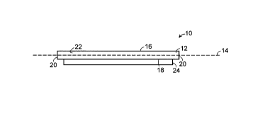
example of which is shown in FIGS 1 and 2. The detector 10 of FIGS. 1 and
2 features a scintillation crystal 12 having a longitudinal axis 14, an input
face 16, an output face 18 opposite the input face 16, end faces 20, and side
faces 22. For multiple channel arrays~ the detectors are sandwiched together
with their side faces adjacent each other and separated by a collim~ting wall
of x-ray absorbing m~t~ri~l which plt;vellts channel cross-talk. The output
face is bonded by means of a transparent agent directly to a silicon
photodiode 24. Examples of such detectors may be found in United States
Patents 4,694,177 issued Sept. 15, 1987 to Akai and 4,725,734 issued Feb.
16, 1988 to Nishiki. A discussion of the general design considerations for
such detectors may be found in Glasow et al's "Aspects of Semiconductor
Current Mode Detectors for X-Ray Computed Tomography" in IEEE
Transaction on Nuclear Science~ Vol. NS-28, No. 1, February 1981, pp. 563-
571.
A typical preselllly-used detector crystal is a rectangaloid bar of
scintill~tor m~teri~l, such as CdWO4, which is 20 mm (millimeters) to 30 mm
long, from 0.5 to 2mm wide and 2 mm to 3 mm thick with end faces which
are perpendicular to the longitudinal axis of the crystal. The thickness of the
bars is det~rmined by the amount of the particular scintillator required to
absorb the x-ray beam; the width of the bar is determined by the resolution
required. The length of the channels is d~ ed by the size of the picture,
or thickness of the "slice", being taken and the response characteristic or
amount of signal deviation allowed. For example, if a 20mm long useful
crystal length is required for a single plane exposure, a 30mm long crystal
21 94942
-
may be required to meet the performance requirements. The bar is made
slightly larger than the photodiode to which it is attached, so that x-rays
c~nnot reach the diode directly and cause unwanted noise in the system. The
end faces 20 extend typically about 0.5 mm beyond the photodiode 24 and
the side faces 22 extend typically about 5% of the width of the crystal 12
over the photodiode 24. For this crystal 12, the useful length for detection
can be considered to be about the middle 20 mm of its length.
The best response of the detector to incident radiation is when the
midpoint of the radiation beam is incident at its axial central. However, in
practice there are deviations of the midpoint of the beam from the midpoint
of the detector, perhaps as a result of vibrations, thermal stress-indl1ced
mi~ nment~ in the equipment, or other factors which may effect the beam
direction. It is a drawback of present scintillation crystals used in conl~uler-ted tomography detectors that when the midpoint of the beam is not
incident on the crystal precisely at its longitudinal midpoint, the
c~Jlle~ollding light output from the crystal to the photodiode may be reduced,
thus yielding a signal which includes a false ~tteml~tion and can result in the
inclusion of erroneous data in the image to be generated. For this reason, it
is the present practice to use only a central segment of the length of the
crystal for receiving the beam, thus requiring a longer crystal. The increased
length of the crystal not only increases the cost of the detector, but also
increases the size of other features of the colll~u~l-assisted tomography
system in which the detector is to be housed. The curve 25 of FIG. 5 is a
graphical representation of the signal strength variation along the longitudinalaxis of the crystal 12 of FIGS. 1 and 2 as an x-ray beam of constant intensity
is moved along the longi~1~1in~l axis from one end of the crystal to the other.
The abscissa indicates the lon~it~1tlin~l position in millimeters. The ordinate
indicates an ~biLIdly m~gnih1de of output signal from the photodiode 24,
with the assumption that there are no serious nonlinearities present. It is seen
21 94~42
-
that only about the central two-thirds of the length has a relatively flat
response.
Summarv of the invention:
The invention addresses the non-uniform response problem of the
detector by redirecting the int~rn~lly-reflected portion of the light created inthe scintillation crystal so that the output response is altered. This is
accomplished by beveling the ends of the crystal to form reflective surfaces
which are non-perpendicular to the longit~l-lin~l axis of the crystal and which
redirect the reflected light in the detector to affect the response curve. In this
manner, the response can be made more uniform for longitudinally varying x-
ray beam positions or can be otherwise altered as desired.
Brief Description of the drawin~s:
FIG. 1 is a front view of a prior art detector.
FIG. 2 is a side view of the detector of FIG. 1
FIG. 3 is a front view of a novel detector having modified ends in
accordance with a prefelled embodiment of the present invention.
FIG. 4 is a side view of the detector of FIG. 3
FIG. 5 is a graph showing the calculated response curve of the
detector of FIGS. 1 and 2.
FIG. 6 is a graph showing the calculated response curve of the
detector of FIGS. 3 and 4.
FIG. 7 is a graph showing the calculated light output of the detector of
FIGS. 3 and 4 which is due to only int~rn~lly reflected light from the
modified ends.
FIG. 8 is a graph showing the response of the graph of FIG. 7 as
adjusted to account for int~.rn~l reflection losses.
FIG. 9 is a graph showing data plots comparing the responses of the
- 21 q4942
detector of FIGS. 1 and 2 and the detector of FIGS. 3 and 4.
FIG. 10 is a front view of the prior art detector of FIGS 1 and 2
showing vectors for calculating the theoretical light response.
FIG. 11 is a front view of the detector of FIGS. 3 and 4 showing
vectors for calculating the theoretical light response attributable to reflections
from the modified ends.
Description:
In accordance with the present invention, a novel detector 26 shown in
FIGS. 3 and 4 comprises a scintillation crystal 28 bonded with a transparent
bonding agent to a photodiode substrate 24. The crystal 26 is a right
rectangaloid which has an input face 16, an output face 18 opposite and
parallel to the input face 16, end faces 20, and m~ lly parallel side faces 22.
The ends additionally have reflecting bevel surfaces 30. The crystal 28 is of
cadmium tllng~t~te. It has a thickness "B" of 2.5 cm (centimeters), a length
"C" of 30 cm, and a useful length "D" of 20 cm. The ends extend beyond
the ends of the photodiode substrate 24 by a distance "A" of 0.5 cm. The
photodiode substrate 24 has a length "E" of 29 cm. The width of the crystal
28 is 1.5 cm. The width of the photodiode substrate 24 is 10% less than that
of the cyrstal 28, so that there is a 5% overhang of the crystal 28 on each
side of the photodiode substrate 24
The bevel surfaces 30 form reflecting facets oriented at 45 degrees to
the output face 18 and exten(lin~ from a shoulder 32 which is 1 mm above
and parallel to the output face 18. The bevel surfaces 30 result in intern~l
reflection modes in the crystal 26 which flatten out the light response to the
photodiode 24, so that more of the length of the crystal may be actively used
to receive the beam. This permits the use of shorter crystals, thereby
reducing both the cost and size of the detector. The light response for the
crystal 26 is shown by the curve 34 in the graph of FIG. 6.
21 q4q42
It can be shown, as is discussed below, that when a light scintillation
event occurs in the center of the crystal of the novel detector 26 of FIGS. 3
and 4, the response curve of the light reflected int~rn~lly from the modified
ends taken alone is represented by the curve 36 which appears in the FIG. 7,
in which again the abscissa is the location in millimeters along the rod, while
the ordinate is the photodiode output. After taking into account an int~rn~l
~tt~ml~tion of about 50%, the resulting response curve 38 of FIG. 8,
norm~li7e~1 with the ordinate values of the response curve 25 of FIG. 5, is
shown as the curve 34 in FIG. 6. The curve 40 of FIG. 9 shows a plot of the
actual output values for the detector 10 of FIGS. 1 and 2 without the bevel
surfaces 32 of the invention as compared to the curve 42 showing the actual
output values for the detector 26 of FIGS. 3 and 4 with the bevel surfaces 32
according to the invention.
While the detector crystal 28 of the above embodiment is of cadmium
tlmg~t~te, it may also be of other suitable scintill~ting material, such as
sodium iodide, calcium fluoride, or bismuth germin~te and derive similar
benefits from the invention. Also, while the optical conversion device of the
described embodiment is a solid state photodiode, it should be understood that
any suitable device for performing the conversion of optical signals to
electrical ones could be used.
The size of the bevel surface effects the output response. Therefore, it
should be chosen to effect the response as is desired for a particular
application, based on the optical principles involved in the light response
analysis described in detail below. The bevel surface could conceivably
include the entire end faces, if necessary. However, for a bevel surface at 45
degrees, such as for the crystal 28, this would leave a relatively fragile edge
at the output face of the crystal. Therefore, the bevel surface is preferably
started a small distance up from the output face. The bevel surface may be
any angular orientation which is non-perpendicular to the longitudinal axis of
21 94~42
-
the crystal in order to effect the desired modification of the response of the
detector. There may be a plurality of such bevel surfaces provided at one or
both ends which are specifically designed to shape the response a certain way
for a particular application, for example where a response other than one
optimized for flatness is desired. The present invention permits deliberate
modification of the response by appropl;ate orientation and sizing of faceted
surfaces at one or both ends of the crystal. The a~plopliate orientation and
sizing of such faceted surfaces can be readily established by an analysis of
the int~rn~l reflections by known analytical techniques such as are described
below.
Li~ht Response Analysis
The light response for the novel detector 26 of FIGS. 3 and 4 can be
analyzed as follows:
It is assumed for the purposes of the analysis that the photons are
emitted and radiate outward in all directions from a point directly in the
center of the bar over the spot where the x-rays enter. The problem is to find
the output as the point of stimulation moves longitudinally along the bar. If
the photons are emitted uniformly in all directions, then the magnitude of the
output is proportional to the size of the acute angle between the vectors Vl
and V2 as shown in Figure 10.
The definition of the dot product for the vectors Vl and V2 gives the
angle "~" between the vectors. A coordinate axis system will be put in place
and the vectors will be calculated as shown below:
Vl=(A,O)-(X l/2B)
Vl=(A-X)i-l/2Bj
V2=(C-A,O)-(X l/2B)
V2= (C-A-X)i-l/2Bj
Once this is done, the definition of the dot product is used.
21 94942
Definition of the dot product:
A vector A dotted with another vector B is equal to the cosine of the
angle 0 between the vectors multiplied by the product of their m~gnil~ldes, or
AB=COS Ox(AB)
When this operation is p~;lrolllled for a detector with tlimen~ions A, B, C as
for the detector 10 above, the following general equation results:
~ = cos-l {(X2-CX+D)(X4+EX3+FX2+GH+H)-"2 }
where D = AC A2 IhB2
E = -2C
F= I/2B2-2A2+2AC+C2
G = 2CA2 l/2Cg2 2C2A
H = l/l6B4+ I~B2C2+l/2B2A2- l/2g2Ac+A2c2+A4 2A3C
Substil~lting the (1imen~ions for the detector 10 for A, B, and C, the followingequation results:
~ = COS-l~(X2-30X + 16.3125)
(X4-60X3+932.625X2-978.75X+1580.160156)-l/2}
The graph of this equation is the graph of FIG. 5.
To reduce the deviation between the end points of this graph and the
center, 45 angles are cut on the edges of the detectors as shown for the
detector 26 of FIGS. 3 and 4. It will now be shown m~tl~em~tically that
these angled corners will help reduce the dirrercnce between the end points
and the center.
Again, the same assumption as before will be made, namely that the
light is emitted uniformly in all directions from a spot in the center of the bar.
21 ~4942
It can be shown that the bevel surfaces actually help decrease the deviation in
the detector. It will be assurned that the light that is reflected into the
photodiode 24 is directly proportional to the light that hits the reflecting
sllrf~res. Therefore, all that must be done is to calculate the magnitude of
light that impacts on the reflective surfaces as the stimulation point changes.
This will be done in exactly the same way using the definition of the dot
product and setting up a coordinate axis system. This time however there
will be two sets of vectors instead of one. The angle between each set will
be added together to give the total m~gni~lde of light that impacts on the
reflecting bevel surfaces from any one emission spot in the bar. The setup is
shown in Figure 11.
V3=(28.5, 2.5)-(X, 1 25) V4=(30,1)-(X,1 25)
V3(28.5-X)i+1.25j V4=(30-X)i-.25j
V1=(0,1)-(X,1.25) V2=(1.5, 2.5)-(X,1.25)
V1=-Xi-.25j V2=(1.5-X)i+1.25j
Using the definition of the dot product, the following equations are obtained:
~ = COS-I{(X2-1.5 X-.3125)(X4-3X3+3.875X2-.1875X+.23828125)
-1/2}+
COS-I{(X2-58.5X+854.6875)(X4-l 17X3+5133.875X2-
100132.3125X+732482.1 1328125)-1/2}
Combining the two, the output is shown on graph of FIG. 7. It can be seen
that this graph varies inversely to the original. The light intensity is greater at
the edges and has a llfil~illlulll value in the middle exactly the opposite to that
~ 21 94942
of the graph of FIG. 5, thus proving that the angled edges will help reduce
the deviation of the output. The amount of help depends on what percentage
of light impacting on the angled surfaces is actually reflected to the detector.The higher this percentage is, the less deviation there will be in the total
output to the detector. If it is assumed that 50% of the light impinging on the
beveled surfaces reaches the photodiode 24 of FIGURES 3 and 4, then a
response as shown by the curve 38 of FIG. 8 is generated. When this
response is combined with the output of the normal detector 10 of FIGS. 1
and 2 as shown by curve 25 of FIG. 5, then the resultant response becomes as
is shown by the curve 34 of FIG. 6 for the novel detector 26 of FIGS. 3 and
4.