Note: Descriptions are shown in the official language in which they were submitted.
CA 02195314 2001-07-05
1
DESCRIPTION
Solder Pad For Printed Circuit Boards
Field of the Invention
This invention relates to printed circuit boards, and more specifically to a
solder pad for omni-directional non-occluding through-holes on printed circuit
boards.
Background of the Invention
The use of a substantially C-shaped solder pad, with plated via holes for
providing an electrical connection between various layers of a printed circuit
board,
wherein the C-shaped solder pad partially surrounds a non-plated through-hole
which
is resistant to solder occlusion upon wave soldering is known in the art and
is
disclosed in U.S. Patent No. 4,851,614 ('614 patent). The use of a spoked
solder pad
is also know in the art.
Although these prior art solder pad designs tend to prevent the occlusion of
solder in the printed circuit board through-holes, these designs also have
some
performance drawbacks which, up to this point, have not been addressed.
The C-shaped solder pad design of U.S. Patent No. 4,581,614 is an
asymmetric design with a preferred orientation. As stated in column 3, lines
24-26 of
the '614 patent, the pad "is substantially C-shaped with the open portion
oriented such
that it is the first portion contacted by the solder when the board is wave
soldered".
It has been discovered that the thickness of the solder adhering to the C-
shaped solder pad varies if the orientation of the C-shaped solder pad design
deviates
from the preferred orientation, or from a predetermined orientation. In other
words,
the only way to ensure that variations in the solder thickness will not occur
is to make
sure that every C-shaped solder pad surrounding every
R'O 96105713 z ~ 9 '~ GI- PC1Y1JS95109791
2
through-hole_required to be non-occluding on every printed
circuit board undergoing the wave soldering process is
oriented with the opening in the "C" shape facing in the
same direction. To ensure that every C-shaped solder pad
is properly oriented adds time and expense to the design
of the printed circuit board because of necessary
coordination with manufacturing to predict the required
orientation. -
If all of the C-shaped solder pads are not properly
oriented, then the variations in thickness that occur,
while minor-can create problems in certain applications
due to the precise tolerance requirements necessary when
developing printed circuit boards for-:.certain uses, such
as in portable computers.
These variations in thickness raise other concerns as
well. For example, when mounting the printed circuit
board to a computer system chassis, a mounting bolt is
inserted through the through-hole of the printed circuit
board and is then tightened into a corresponding bolt hole
on the chassis. As the mounting bolt is tightened, a
lower surface of a mounting bolt head begins exerting
pressure on the printed circuit board in the region of the
through-hole, as well as on the solder pad located on the
lower surface of the printed circuit board which comes
into contact with the computer-chassis. The thickness of
the solder which comprises the solder pad is uneven around
the through-hole and causes the uneven application of
pressure around the through-hole by the tightening of the
mounting bolt, and such uneven strain placed on the
printed circuit board when the mounting bolt is tightened
can result _in the delamination of the printed circuit
board in the region of the through-hole, as well as the
separation of the solder pad or underlying copper from the
surface of :the printed circuit board. Also, these
thickness variations contribute to mechanical dimensional
tolerances, which may lead to the misalignment of circuit
W096J05713 , , , ,~ PCTlUS95/09791
3
components on-the printed circuit- board to associated
mechanical components on the computer chassis.
Even if there are no variations in thickness of the
solder, which assumes proper orientation of the solder
pads, the asymmetric design of the C-shaped solder pad
inherently leads to the possibility of uneven pressures
being applied to the printed circuit board around the
through-hole by the tightening of the mounting bolt.
Since solder attaches only to the unmasked exposed C-
shaped portion of the copper plated ring, while the gap or
opening which defines the "C" shape remains free of
solder, there is inherently an uneven distribution of
solder about the through-hole due to the asymmetry of the
solder pad design. This uneven distribution of solder can
create the same problems of delamination and separation as
discussed above.
As mentioned previously, the use of the spoked solder
pad is known in the art, although applicant does not know
whether the spoked solder pad design was implemented as a
solution to the problems arising from the C-shaped solder
pad design of the prior art, as discussed above.
Regardless, the spoked solder pad designs of the prior art
also have drawbacks which, to this point, have not been
addressed.
By implementing the spoked solder pad design, the
problems of orientation are no longer a concern, since a
symmetric design does not have a preferred orientation,
and the direction of travel over a wave solder does not
matter. In other words, a symmetric design is omni
directional.
However, the apoked solder pad design has a smaller
contact area of solder between the printed circuit board
and the computer chassis than the C-shaped solder pad
design (as shown in comparison in FIG. la and FIG. 1b).
The contact area of solder between the printed circuit
board and the computer chassis via the solder pad serves
the important function of providing an electrical
WO 96105713 ' s l PCT/US95109791
4
connection between the logical ground of the circuit on
the printed circuit board and the electrical ground of the
computer chassis.
Due to the minimal contact area of the spoked solder
pad design, certain drawbacks exist. In certain
aituations, if the contact area of solder on the solder
pad between the printed circuit board and the chassis is
insufficient to create a proper grounding connection, then
the improper grounding which results can cause computer
system errors.
Because of certain regulatory requirements regarding
electro-magnetic interference (EMI) and radio frequency
interference -(RFI), proper grounding is imperative. For
example, high frequency radio frequency (AF) energy must
be adequately-returned to the chassis electrical ground to
prevent excessive radiation from the unit. This is in
order to comply with specified emission levels (measured
in decibels or dB) set by regulatory-agencies. The total
contact area--between the exposed conductive area of the
solder pad and the computer chassis is key to effectively
maximising the conduction of the RF energy to electrical
ground, thereby contributing to the reduction of the
associated dB levels at various frequencies. Analysis of
the C-shaped solder pad design versus the spoked solder
pad design shows that the total surface area of the C-
shaped solder pad design that comes into contact with the
computer chassis is significantly different than that of
the spoked solder pad design.
While the solder pad designs of the prior art do
provide workable solutions to the problem of solder
occlusion, the C-shaped solder pad design has variations
in-thickness problems resulting from variations in the
orientation of the solder pad. Moreover, the spoked
solder pad design has insufficient contact area problems
which can result in an improper grounding connection.
In other words, the C-shaped solder pad design
provides sufficient contact area between the solder pad on
21953.1
WO 96105713 PCT/US95109791
the lower surface of the printed circuit board and the
computer chassis to provide for proper grounding with the
chassis. However, the varying orientation of the
~ asymmetric C-shaped solder pad design as it is passed
5 through the wave solder creates variations in the
thickness of the solder on the solder pad.
On the other hand, while the spoked design does not
have this orientation problem, it does have a drawback in
that there ie insufficient contact area between the solder
pad on the lower surface of the printed circuit board and
the computer chassis to provide for a proper grounding
connection. Therefore, a solution is needed that
addresses all of the problems which currently exist in the
prior art.
Summary of th Invention
The omni-directional non-occluding solder pad of the
present invention has a novel configuration which solves
the problems of the prior art mentioned above, ae well as
the problem of solder occlusion in the through-hole.
The solder pad of the present invention is a
symmetrical design which is omni-directional, and
therefore does not create variations in thickness of
solder as a result of variations in the orientation of the
solder pad as it travels over the wave solder. Thus, this
design permits the even distribution of mounting forces
around the through-hole by providing a level solder pad
surface around the perimeter of the mounting hole.
The solder pad of the present invention comprises a
plurality of spokes displaced from the through-hole in an
outwardly radiating direction. The novel configuration
further comprises a circular ring which is concentric to
the through-hole and intersects the plurality of spokes.
This additional ring structure provides for additional
contact area of solder between the printed circuit board
and the computer chassis thereby increasing the
probability of a proper grounding connection, and
CA 02195314 2001-07-05
6
decreasing the probability of a computer system error resulting from an
insufficient
contact area of solder. The contact area can be varied to suit the particular
application
by changing the width of the solder pad ring and/or spokes.
Accordingly, it is an object of the present invention to provide an improved
solder pad design.
It is a further object of the present invention to provide an omni-directional
non-occluding solder pad design.
An additional object of the present invention is to provide an omni-
directional
non-occluding solder pad design for through-holes on printed circuit boards.
Another object of the present invention is to provided an omni-directional
non-occluding solder pad design that is always properly oriented, and provides
a
sufficient contact area of solder between a printed circuit board and a
computer
chassis for a proper grounding connection.
Yet another object of the present invention is to provide an omni-directional
non-occluding solder pad design that allows for even mounting pressures to be
applied to a printed circuit board in the region of a through-hole, thereby
mitigating
delamination and separation problems, as well as mechanical alignment
problems.
According to an aspect of the present invention, there is provided a printed
circuit board having at least one through-hole and comprising:
a conductive ring disposed about and displaced from said through-hole
through said printed circuit board,
a plurality of conductivity plated via holes passing through said printed
circuit
board at the location of said conductive ring, and
a solder mask covering portions of said conductive ring adapted such that
passing unmasked portions of said conductive ring over a wave solder creates a
solder
pad comprising a plurality of spokes radiating outward from said through-hole,
said
spokes intersecting a circular ring concentric to said through-hole at
approximately a
perpendicular angle.
According to another aspect of the present invention, there is provided a
laminated printed circuit board having at least one through-hole comprising:
a plurality of conductor-containing layers,
a solder pad surrounding said through-hole comprising:
CA 02195314 2001-07-05
6a
a plurality of spokes radiating outward from said through-hole, said spokes
intersecting a circular ring concentric to said through-hole at approximately
a
perpendicular angle,
said solder pad being on an external layer of said printed circuit board
disposed about said through-hole through said printed circuit board, and
a plurality of via holes through said printed circuit board at the location of
said
solder pad, said via holes having a plated bore electrically interconnecting
said solder
pad with selected conductors on other layers of said printed circuit board.
According to another aspect of the present invention, there is provided a
printed circuit board having at least one through-hole comprising:
a conductive ring surrounding said through-hole through said printed circuit
board,
a plurality of via holes through said conductive ring, and
a solder mask covering portions of said conductive ring adapted such that
passing unmasked portions of said conducive ring over a wave solder creates a
solder
pad comprising a plurality of spokes radiating outward from said through-hole,
said
spokes intersecting a circular ring concentric to said through-hole at
approximately a
perpendicular angle.
According to another aspect of the present invention, there is provided a
method of manufacturing a printed circuit board having at least one through-
hole
surrounded by a conductive ring comprising the steps of:
placing a solder mask on portions of said conductive ring,
passing said printed circuit board over a wave solder, and
adhering solder to unmasked portions of said conductive ring such that said
solder forms a solder pad disposed about said though-hole through said printed
circuit
board with a plurality of via holes through said printed circuit board at the
location of
said solder pad, said solder pad comprising a plurality of spokes radiating
outward
from said through-hole, said spokes intersecting a circular ring concentric to
said
through-hole at approximately a perpendicular angle.
According to another aspect of the present invention, there is provided a
printed circuit board having at least one through hole, an upper layer, and a
lower
layer, comprising:
a conductive ring on said upper layer of said printed circuit board,
CA 02195314 2001-07-05
6b
a solder pad located on said lower layer of said printed circuit board
disposed
about and displaced from said through-hole through said printed circuit board,
said
solder pad comprising a plurality of spokes radiating outward from said
through-hole,
said spokes intersecting a circular ring concentric to said through-hole at
approximately a perpendicular angle, and
a plurality of plated via holes electrically interconnecting said solder pad
on
said lower layer to said conductive ring on said upper layer of said printed
circuit
board.
According to another aspect of the present invention, there is provided a
printed circuit board, having am upper layer and a lower layer, comprising:
at least one through-hole through said printed circuit board,
a solder pad located on said lower layer of said printed circuit board
disposed
about and displaced from said through-hole through said printed circuit board,
said solder pad comprising a plurality of spokes radiating outward from said
through-hole, said spokes intersecting a circular ring concentric to said
through-hole
at approximately a perpendicular angle,
a pad of conductive material on said upper layer of said printed circuit board
disposed about and displaced from said through-hole though said printed
circuit
board, and
a plurality of plated via holes passing though said solder pad and
electrically
interconnecting said solder pad on lower layer to said pad of conductive
material on
said upper layer of said printed circuit board.
According to further aspect of the present invention, there is provided an
electronic assembly comprising:
an electrically conductive chassis,
a printed circuit board comprising at least one through-hole,
a solder pad disposed about and displaced from said through-hole through said
printed circuit board, said solder pad comprising a plurality of spokes
radiating
outward from said through-hole, said spokes intersecting a circular ring
concentric to
said through-hole at approximately a perpendicular angle, and
a mounting bolt for attaching said printed circuit board to said chassis, said
mounting bolt passing through said through-hole having said solder pad
disposed
about it, and electrically bonding said chassis to said solder pad.
CA 02195314 2001-07-05
6c
Further objects and advantages of the present invention will become apparent
from a consideration of the drawings and ensuing description.
Description of the Drawing-s
FIG. 1 a is an illustration of a C-shaped solder pad of the prior art
surrounding
a through-hole.
FIG. 1b is an illustration of a spoked solder pad of the prior art surrounding
a
through-hole.
FIG. 2a is a perspective view of a portion of a printed circuit board and a
portion of a computer chassis.
~iVi~py.~_~...~~__... ..............e.._ _._.__"...._ ...._.._...
R'O 96/05713 ; ~ . PGTIUS95I09791
7
A through-hole on the printed circuit board is shown in a
' cutaway view.
FIG.-2b is a view of the through-hole, shown from the
point-of-view of the computer chassis, looking up at a
lower layer of the printed circuit board. The through
hole has an improved omni-directional non-occluding solder
pad design surrounding it on the lower layer of the
printed circuit board. Typically, the solder pad design
is only needed on the wave solder side of the printed
circuit board, which is usually the lower layer of the
printed circuit board that ultimately contacts the
computer chassis.
FIG. 3 is a perspective view of a non-plated through-
hole surrounded by a copper plated ring.' The copper
plated ring is placed on both the upper layer and the
lower layer of the printed circuit board, and is displaced
from the outer edge of the through-hole. The upper layer
and the lower layer copper plated rings are electrically
interconnected by copper plated via holes.
This configuration is known in the prior art, and the
term "copper plated" is understood by those ofordinary
skill in the art to refer to either bare copper or copper
with additional plating or protective coating. The
protective coating can be a non-metallic chemical coating
used to temporarily protect the bare copper from oxidation
before use. This protective coating is typically removed
during the manufacturing process.
FIG. 4a is an illustration of the solder mask
clearance design.
FIG. 4b is an illustration of a solder mask design
which- overlays the lower layer copper plated ring and
allows specific areas of the copper plated ring, in the
shape of a solder mask clearance design (as shown in FIG.
4a), to remain exposed to the wave soldering process,
whereby the'solder attaches to the unmasked portions.
FIG. 5 is a perspective view of the solder mask design
overlaid onto the structure of FIG. 3, whereby the exposed
wo 9siosm3 Z 7 95 3 7 4- PCT/US95/0979i
8
portions of the copper plated ring is in the shape of the
solder mask clearance design of FIG. 4a:'
FIG. 6 is a top view of the solder pad around the
through-hole, as it appears after being wave soldered.
T~Pra~ied Description Of A Preferred Embodiment
FIG. la shows a C-shaped solder pad design and FIG. 1b
shows a spoked solder pad design, both of which are known
in the prior art.
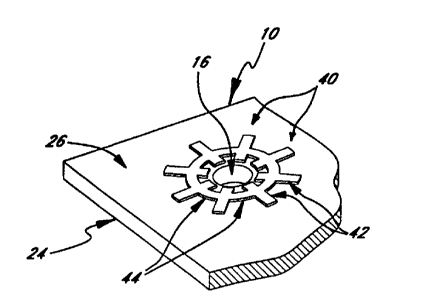
FIG. 2a shows a portion of a printed circuit board 10
and a portion of a computer chassis 12. The printed
circuit board 10 comprises circuit components 14, and at
least one non-plated through-hole 16 which can be used as
a mounting hole, also known as a chassis ground mounting
hole.
FIG. 2b shows a lower layer 26 side of the through-
hole 16 shown from the bottom of the printed circuit board
I0, or from the point-of-view of the computer chassis 12
looking up at the bottom of the printed circuit board 10.
A solder pad 40 is shown located around the through-hole
16 on the lower layer 26 of the printed circuit board 10.
The process for placing the solder pad 40 around the
through-hole 16 is discussed in further detail below.
Referring now to FIG. 2a and 2b, the printed circuit
board 10 is typically mounted to the computer chassis 12
by inserting a mounting bolt 18 through the through-hole
16 of the printed circuit board 10, and then tightening
the mounting bolt 18 into a corresponding bolt hole 22 on
the computer chassis 12. As the mounting bolt 18 is
tightened, a lower surface 19 of a mounting bolt head 20
begins exerting pressure on the printed circuit board l0,
as well as a copper plated ring 30 (shown in FIG. 3) on an ,
upper layer 24, and the solder pad 40 on the lower layer
26 of the printed circuit board i0 around the through-hole
16.
FIG. 3 shows the non-plated through-hole 16 surrounded
by the copper plated ring 30, with a plurality of copper
R'O 96105713 PC1YOS95109791
9
plated via holes 32 through the printed circuit board 10
at the location of the copper plated ring 30. The copper
plated ring 30 is placed on both the upper layer 24 and
the lower layer 26 of the printed circuit board 10 and is
displaced from the outer edge of the through-hole 16. The
upper layer 24 copper plated ring 30 and the lower layer
26 copper plated ring 30 are electrically interconnected
by copper plated via holes 32. This configuration is
known in the prior art.
FIG. 4a shows a solder mask clearance design 36
comprising a plurality of spokes 42 and a ring 44
concentric to the through-hole 16. The spokes 42 radiate
outward from the through-hole 16 so as to intersect the
ring 44 at approximately a perpendicular angle. The
solder mask clearance design 36 represents the portions of
the printed circuit board 10 (FIG. 1) that remain unmasked
by a solder mask design 34 (shown in FIG. 4b). The solder
mask clearance design 36 is used to indicated the shape
that the solder pad 4D (FIG. 2b) will take after the wave
soldering process, since the solder pad 40 adheres only to
the unmasked portions of the printed circuit board 10.
FIG. 4b shows the solder mask design 34. This design
is basically the inverse of the solder mask clearance
design 36, since the solder mask design 34 indicates the
portions of the printed circuit board 10 that will be
masked, whereas the solder mask clearance design 36
indicates the portions of the printed circuit board 10
(FIG. 1) that will remain unmasked. The solder mask
design 34 comprises a plurality of arcuate trapezoidally
shaped segments 35 placed in a concentric pattern about
the through-hole 16 such that the gaps between these
segments 35 define the shape of the solder mask clearance
design 36 (FIG. 4a), as well as the solder pad 40 (FIG.
2bj .
The, solder mask design 34 of FIG. 4b is overlaid on
the copper plated ring 30 (FIG. 3) located on the lower
layer 26 of the printed circuit board 10 such that passing
R'0 96105713 ~ ~ 9 5 3 I 4 PCTIUS95I09791
the printed circuit board 10 over a wave solder results in
the adherence.of solder to the unmasked portions of the
printed circuit board 10, which typically comprises
portions of the copper plated ring 30 in the region of the -
5 through-hole ..16 on the lower layer 26.- These unmasked
portions expose portions of the copper plated ring 30 in
the shape of the solder mask clearance design 36, thereby
generating the solder pad 40 of a similar shape when the
printed circuit board 10 is passed over the wave solder.
10 In other words, the solder mask design 34 indicates
the portions-of the printed circuit board 10 that resist
solder, whereas the solder mask clearance design 36
indicates the portions of the printed circuit board 1D
where solder will adhere. Therefore, when the solder mask
design 34 overlays the copper plated ring 30, thereby
allowing the unmasked areas of the copper plated ring 30
to remain exposed to the wave solder, the solder attaches
to those exposed copper portions of the copper plated ring
3D to form the solder pad 40 in the shape of the solder
mask clearance design 36.
The resulting solder pad 40 comprises the plurality of
spokes 42, and the ring 44 concentric to the through-hole
16. The spokes 42 radiate outward from the through-hole
16 so as to intersect the ring 44 at approximately a
perpendicular angle. The. copper plated via holes 32 fill
with solder during the wave soldering process via
capillary action -in--a manner understood by those of
ordinary skill in the art. In a preferred embodiment, the
copper plated via holes 32 are ..located at the
intersections of the spokes 42 and the ring 44.
The solder mask design 34 is needed only on the lower
layer 26 of the printed circuit board-10 to produce the , ,
solder pad 4D on the lower layer -26 which provides a
contact area that serves as an electrical connection
between theprinted circuit board IO and the computer
chassis 12. The upper -layer 24 of the printed circuit
board 10 does not require the solder pad 40.
WO 96105713 ~ ~ ~ ~ ~ "~ ~ PC1YUS95109791
11
FIG. 5 shows the solder mask design 34 -(FIG. 4b)
comprising the segments 35 overlaid onto the copper plated
ring 30. This is how the printed circuit board 10 appears
before being passed over the wave solder. When the solder
mask design 34 comprising the segments 35, the copper
plated ring 30, and the copper plated via holes 32
(collectively hereinafter called a pad design 38), are
passed over the wave solder, the pad design 38 allows the
non-plated through-hole 16 to remain free of solder
occlusion after traveling through the printed circuit
board 10 circuit component 14 attachment step of-the wave
soldering process. During the wave soldering process, the
solder adheres to the exposed copper areas of the copper
plated ring 30 around the through-hole 16 in the shape of
the solder mask clearance design 36.
FIG. 6 shows the solder pad 40 around the through-hole
16, as it appears after the wave soldering process. Note
that the unmasked portions of the copper plated ring 30
(FIG. 5) now comprise the solder pad 40. '
As a result of the symmetrical design of the resulting
solder pad 40, there is no need for ensuring proper
orientation of the solder pad 40 since the symmetric
solder pad 40 is omni-directional. Furthermore, the
addition of the ring 44 structure provides additional
contact area of solder which serves as an electrical
connection between the printed circuit board 10 and the
computer chassis 12. This additional contact area
provides sufficient electrical connection between the
printed circuit board 10 and the computer chassis.l2 to
ensure a proper grounding connection.
While the above description contains many
specificitiea, these should not be construed as
limitations on the scope of the invention, but rather as
an exemplification of one preferred embodiment thereof.
Many other variations are possible. For example, the
number of spokes 42 and the number of copper plated via
holes 32 can be varied without significantly affecting the
WO96l05713 Z~ C~ 57~. '~ 4 PCfIUS95/09791
12
operation of-the present invention. Furthermore, the
location of the copper plated via holes 32 can be located
in various positions on the spokes 42 or on the ring 44,
and not necessarily at the intersections of the spokes 32
and the ring 44. In addition, the copper plated ring 30
and the copper plated via holes 32 can be plated with
conductive materials other than copper that provide an
electrical connection between the various layers of the
printed circuit board 10. Also, the diameter of the
copper plated via holes 32 can be varied such that, if the
through-hole 16 were conductively plated, the total
conductive area of the collective copper plated via holes
32 would be equal to or greater than the relative
conductive area of the through-hole 16.