Note: Descriptions are shown in the official language in which they were submitted.
CA 02195438 2000-02-16
- 1 -
DESCRIPTION
OPTICAL CARD WITH A BUILT-IN IC MODULE
TECHNICAL FIELD
The present invention relates to an optical card with
built-in IC module, having a recording part of an optical
recording system (hereinafter referred to as "optical
recording part") and an IC module.
BACKGROUND ART
Information recording cards have become used
prevalently in recent years, and active R&D activities have
been made to develop optical cards having a large capacity
which may replace magnetic cards and IC cards. There have
been proposed what they call heat mode recording materials
as optical recording materials for forming the recording
layer of the optical card. The recording layer of a heat
mode recording material is scanned with a spot of an energy
beam, such as a laser beam, to change the state of portions
thereof for recording. The heat mode recording material is
a metal thin film, such as a bismuth thin film, an organic
thin film, such as a polystyrene thin film or a
nitrocellulose thin film, or a low-valence tellurium oxide
film subject to phase transition when exposed to heat.
Those optical recording materials do not need any
subsequent treatment, such as a developing treatment, after
information has been written thereto, and information
written thereto can be verified after writing. An optical
card provided with such an optical recording material is a
DRAW (direct read after write) medium which is capable of
high-density recording, has a large capacity and-allows
additional writing.
In the optical card having an optical recording part of
such an optical recording material, information once
written to the optical recording part cannot be changed.
Therefore, a new storage area is used every time data to be
successively changed, such as a directory of recorded data
(retrieval information) or a FAT (file allocation table),
CA 02195438 2000-02-16
- 2 -
is written to the optical recording part and thereby a data
storage area available for storing essential data is
reduced. With such a problem in view, there has been
proposed an optical card with a built-in IC module formed
by mounting an IC module having an IC chip on an optical
card, and capable of storing data which is to be rewritten,
such as a directory or a FAT, in the IC module.
When reading data from such an optical card with a
built-in IC module, a host computer needs only to specify
a file name, and a card drive makes a quick electrical
access to the IC chip, retrieves a directory, and records
a track number indicating a track on which the specified
data file is written. Subsequently, an optical pickup
makes an access to the track of the optical recording part
to read the specified data file. If format is
standardized, the optical card with a built-in IC module
can freely be used in all network systems. Although the
optical recording part is not rewritable, data which needs
rewriting are recorded on the IC chip because the IC chip
is relatively easily rewritable.
Generally, the optical card with a built-in IC module
employs an IC chip with a built-in CPU combined with an IC
memory. An IC module included in such an optical card with
a built-in IC module has a base, an IC chip formed on the
base, and a terminal part formed on the base. The
terminals of the terminal part of the IC module are brought
into contact with a contact head included in a read/write
(R/W) device to connect the IC module electrically to the
R/W device so that I/O lines are established. Information
is read and written through the I/O lines. The internal
CPU of the IC chip performs advanced decisions and
operations to maintain the security of the information.
The optical card with a built-in IC module having the
optical recording part and the IC module is thin and its
thickness is standardized (0.76~0.08 mm, ISO Standards) and
the optical recording part is required to be installed at
a standard depth of 0.4~0.05 mm from the surface of the
CA 02195438 2000-02-16
- 3 -
optical card. The R/W device for writing information to
and reading information from the optical recording part is
constructed so as to meet those standards. The horizontal
position of the optical recording part with respect to the
right side, the left side and the lower side of the optical
card is specified in ISO Standards (ISO 11694-2).
According to ISO Standards, the distances from the right
and the left edge of the optical card to the ends of a
region for the optical recording part must be 3 mm or less,
and the distance from the lower edge of the optical card to
the end of the same region must be 4.5 mm or less.
Therefore, an area taken by the optical recording part
needs to be expanded toward the upper edge of the optical
card to increase the capacity of the optical recording
part.
Thus, the region for the optical recording part needs
to be expanded to a terminal region for the terminal part
of the IC module specified in ISO Standards (ISO 7816-2)
for IC modules, to increase the capacity of the optical
recording part of the optical card with a built-in IC
module. If the region for the optical recording part is
expanded, the optical recording part and the IC module
overlap each other and, since the thickness of the IC
module is about 0.6 mm, the thickness of a contact region
of the optical card increases beyond the standard thickness
of 0.76~0.08 mm specified in ISO Standards, so that the IC
module should not penetrate the optical recording film.
DISCLOSURE OF THE INVENTION
The present invention has been made in view of those
problems and it is therefore an object of the present
invention to provide an optical card with a built-in IC
module, allowing effective increase in the capacity of an
optical recording part to be employed therein and capable
of suppressing increase in the thickness of its component
optical card.
According to a first aspect of the present invention,
an optical card with a built-in IC module comprises a base
CA 02195438 2000-02-16
- 4 -
card, an optical recording part mounted on the base card,
and an IC module mounted on the base card. The IC module
includes a base, an IC chip unit attached to one surface of
the base, and a terminal part formed on the other surface
of the base. The terminal part of the IC module is
disposed so as to be exposed to the outside, the IC chip
unit is disposed in a region of the base card other than a
region in which the optical recording part is disposed.
According to a second aspect of the present invention,
the IC chip unit on one of the surfaces of the base, and
the terminal part on the other surface of the base are
disposed in regions of the base card not corresponding to
each other.
According to a third aspect of the present invention,
the area of the terminal part of the IC module is greater
than that of the IC chip unit, and the IC chip unit is
disposed within a region corresponding to the terminal
part.
According to a fourth aspect of the present invention,
the base of the IC module overlaps the region corresponding
to the optical recording part, and a pair of opposite end
edges of the base lie outside a region corresponding to the
optical recording part.
According to a fifth aspect of the present invention,
the base of the IC module overlaps a region corresponding
to the optical recording part, an edge of the base extends
linearly in a region corresponding to the optical recording
part at a predetermined inclination to the direction in
which tracks of the optical recording part extend.
According to a sixth aspect of the present invention,
the base of the IC module overlaps a region corresponding
to the optical recording part, edges of the base of the IC
module overlap a region corresponding to the optical
recording part, and an edge of the base extends
curvilinearly in a region corresponding to the optical
recording part.
According to a seventh aspect of the present invention,
CA 02195438 2000-02-16
- 5 -
the base card includes a base plate for the terminal part,
and a base plate for the optical recording part, and a
covering layer of substantially the same color as that of
the base plate for the terminal part is formed on the back
surface of the IC chip unit of the IC module.
According to an eighth aspect of the present invention,
the base card includes a base plate for the terminal part,
and a base plate for the optical recording part, and the IC
chip unit of the IC module includes an IC chip and a
sealing resin molding for encapsulating the IC chip
therein, and the color of the sealing resin molding is
substantially the same as that of the base plate for the
terminal part.
According to the first aspect of the present invention,
as the optical card with a built-in IC module in accordance
with the present invention has the IC chip unit disposed in
the region outside the region in which the optical
recording part is disposed, the region for the optical
recording part can be expanded without entailing increase
in the thickness of the base card.
According to the second aspect of the present
invention, as the IC chip unit and the terminal part are
disposed in regions other than the corresponding regions,
the IC chip unit and the optical recording part can be
disposed so as not to overlap each other with the terminal
part disposed at a predetermined position.
According to the third aspect of the present invention,
as the IC chip unit is disposed in a portion of the region
corresponding to the terminal part, the IC chip unit and
the optical recording part can be disposed so as - not to
overlap each other with the terminal part disposed at a
predetermined position.
According to the fourth aspect of the present
invention, as the pair of edges of the base lie outside the
region corresponding to the optical recording part, the
optical recording part will not be damaged even if stress
is concentrated on portions in the vicinity of the pair of
CA 02195438 2000-02-16
- 6 -
edges when the optical card is bent.
According to the fifth aspect of the present invention,
as the edge of the base is extended at a predetermined
inclination to the direction in which tracks of the optical
S recording part extend, the tracks of the optical recording
part will not be damaged by stress concentration on
portions in the vicinity of the edge even if stress is
concentrated on portions in the vicinity of the edge of the
base when the optical card is bent.
According to the sixth aspect of the present invention,
as the edge of the base extends curvilinearly, the tracks
of the optical recording part will not be damaged by stress
concentration on portions in the vicinity of the edge even
if stress is concentrated on portions in the vicinity of
the edges of the base when the optical card is bent.
According to the seventh and the eighth aspect of the
present invention, the back surface of the IC chip unit can
be concealed by the covering layer or the sealing resin
molding in the base plate for the terminal part from view
when the optical card is observed from the side of the base
plate for the optical recording part.
BRIEF DESCRIPTION OF THE DRAWINGS
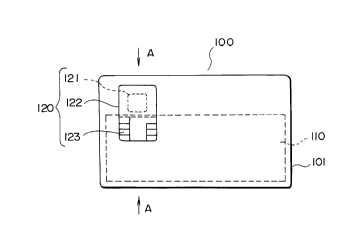
Fig. lA is a plan view of an optical card with a built
in IC module in a f first embodiment according to the present
invention;
Fig. 1B is a rear view of the optical card with a
built-in IC module of Fig. lA;
Fig. 1C is a sectional view taken on line A-A in Fig.
1A;
Fig. 2A is a plan view showing the disposition of an IC
module;
Fig. 2B is a plan view of an IC module provided with a
dummy terminal;
Fig. 3 is a schematic sectional view of assistance in
explaining a manufacturing process for manufacturing an
optical card with a built-in IC module;
Fig. 4A is a plan view of a common IC module;
CA 02195438 2000-02-16
- 7 _
Fig. 4B is a sectional side view of the IC module of
Fig. 4A;
Fig. 5A is a plan view of an optical card with a built-
in IC module in a second embodiment according to the
present invention;
Fig. 5B is a sectional view taken on line B-B in Fig.
5A;
Fig. 6 is a plan view showing the disposition of an IC
module;
Fig. 7 is a plan view of an IC module having a dummy
terminal;
Fig. 8 is a schematic sectional view of assistance in
explaining a manufacturing process for manufacturing an
optical card with a built-in IC module;
Fig. 9A is a plan view of an optical card with a built-
in IC module in a third embodiment according to the present
invention;
Fig. 9B is a rear view of the optical card with a
built-in IC module of Fig. 9A;
Fig. 9C is a sectional view taken on line C-C in Fig.
9A; and
Fig. 10 is a plan view of an optical card with a built-
in IC module in a modified embodiment according to the
present invention.
BEST MODE FOR CARRYING OUT THE INVENTION
First Embodiment
A first embodiment of the present invention will be
described hereinafter with reference to the accompanying
drawings. Figs. lA to 4B show an optical card with a
built-in IC module in a first embodiment according to the
present invention.
A common IC module will be explained with reference to
Figs. 4A and 4B. Referring to Figs. 4A and 4B, an IC
module 120 has a base 122. An IC chip 121a including a CPU
and a memory is mounted on a first surface of the base 122,
the electrode pads 161 of the IC chip 121 are connected to
a pattern layer formed on the first surface of the base 122
CA 02195438 2000-02-16
_ g _
by wires 162, respectively. The IC chip 121a and the
associated parts are sealed in a sealing resin molding 121b
to form an IC chip unit 121. A terminal part 123 is formed
on a second surface of he base 122 by a copper foil layer
156, a plated Ni layer 157, i.e., an underlayer, and a
plated gold layer 158. The terminal part 123 is divided by
isolation grooves 163 into a CLK (clock) terminal, an I/O
terminal, a V~~ ( power ) terminal, a RST ( reset ) terminal and
GND ( ground ) terminal . The base 122 is provided with rough
holes for electrically interconnecting a pattern layer 160
formed on the first surface of the base 122 and the
terminal part 123 formed on the second surface of the base
122.
An optical card with a built-in IC module will be
described with reference to Figs. lA to 1C. Referring to
Figs. lA to 1C, an optical card 100 with built-in IC module
comprises a base card 101 including a first base plate 130
and a second base plate 140, an optical recording part 110
formed in the base card 101, and an IC module 120.
As shown in Figs. lA to 1C, the IC module 120,
similarly to the foregoing common IC module 120, has a base
122, an IC chip unit 121 mounted on a first surface of the
base 122, and a terminal part 133 formed on a second
surface of the base 122. The IC chip unit 121 includes an
IC chip 121a and a sealing resin molding 121b. The IC chip
unit 121 may comprises only the IC chip 121a.
The IC module 120 has a terminal part 123 disposed in
a surface of the base card 101 so as to be exposed to view.
The IC chip unit 121 and the terminal part 123 of the IC
module 120 are disposed in different regions, respectively;
that is, the IC chip unit 121 and the terminal part 123 are
disposed substantially symmetrically with respect to the
middle portion of the base 122 as shown in Figs. lA to 1C.
The IC chip unit 121 is disposed on one side of the middle
portion of the base 122 and the terminal part 123 is
disposed on the other side of the middle portion of the
CA 02195438 2000-02-16
_ g -
base 122.
The IC chip unit 121 of the IC module 120 is disposed
in a region outside the optical recording part 110, and the
terminal part 123 is disposed in a region corresponding to
the optical recording part 110.
The terminal part 123 formed on the base 122 is
disposed at a predetermined position on the front surface
of the optical card 100 with a built-in IC module so as to
be connected to an external circuit (read/write device),
i.e., a position in a terminal region specified in ISO
Standards, and the IC chip unit 121 including the sealing
resin molding 121b is disposed at a position in an upper
portion of the optical card 100 spaced from the terminal
part 123 as shown in Fig. lA. The optical recording part
110 is disposed in a region in which the terminal part 123
is disposed and the IC chip unit 121 including the sealing
resin molding 121b is not disposed.
As shown in Fig. 1C, the IC chip unit 121 of the IC
module 120, including the sealing resin molding 121b is
apart from the terminal unit 123. Since the IC chip unit
121 including the sealing resin molding 121b does not
overlap the optical recording part 110, the base card 101
having the first base plate 130 and the second base plate
140 has a thickness equal to that of the base card of a
conventional optical card and within the thickness range of
0.76~0.08 mm specified in ISO Standards.
In the optical card 100 with built-in IC module, the
terminal part 123 of the IC module 120 can be disposed in
the region specified in ISO Standards (ISO 7816-2), the
base card 101 has a thickness within the thickness range of
0.76~0.08 mm specified in ISO Standards, and the optical
recording part 110 can be expanded to the region for the
terminal part specified in ISO Standards (ISO 11694-2).
In the conventional optical card with a built-in IC
module, the IC chip unit 121 including the sealing resin
molding 121b is disposed in a region corresponding to the
terminal part 123 as shown in Fig. 4B. Therefore, if the
CA 02195438 2000-02-16
- 10 -
optical recording part 110 is expanded to the terminal part
123 of the optical card 100, the IC chip unit 121 and the
optical recording part 110 overlap each other and,
consequently, the thickness of the base card 101 increases
and is unable to meet the requirements of ISO Standards.
A read/write device conforming to the requirements of ISO
Standards is unable to deal with such an optical card
having a base card not meeting the requirements of ISO
Standards. The optical card 100 with built-in IC module of
the present invention can be handled by a read/write device
conforming to the requirements of ISO Standards.
The materials of the base card 101 will be explained
hereinafter. The first base plate 130 and the second base
plate 140 of the base card 101 are made of a polycarbonate
resin and a polyvinyl chloride resin, respectively. The
thickness of a portion of the first base plate 130
corresponding to an optical memory region llla (Fig. 3) is
0.4~0.05 mm. The first base plate 130 does not have any
optical strain and has a transmittance of 950 or above to
light radiations of a wavelength in the range of 750 to 850
nm. Suitable materials other than the polycarbonate resin
for forming the first base plate 130 are polystyrene
resins, amorphous polyolefin resins, polyester resins,
acrylic resins, polyvinyl chloride resins, epoxy resins and
such.
Suitable materials other than the polyvinyl chloride
resin for forming the second base plate 140 are ABS resins,
polycarbonate resins and such.
The optical recording part 110 is formed by covering a
rugged recess 111 having a rugged bottom surface with an
optical recording layer 112 of a tellurium-base metallic
optical recording material. The optical recording layer
112 may be formed of a material other than the tellurium
base metallic optical material. The optical recording
layer 112 may be formed of a material to which information
is written and from which information is reproduced by a
light beam, such as a laser beam emitted by a semiconductor
CA 02195438 2000-02-16
- 11 -
laser, and in which a photochemical reaction as a recording
mechanism takes place, what they call a heat mode recording
material which generates heat upon absorption of light and
carries out a recording mechanism or any other material,
provided that the material is capable of changing its
reproducing light reflecting and transmitting
characteristics when information is written thereto and of
enabling reading the information written thereto.
A hard coating layer 113 is formed over the outer
surface of the first base plate 130 to protect the optical
recording part 110 from being scratched and damaged. The
hard coating layer 113 is formed of a UV-setting acrylic
resin. The hard coating layer 113 may be formed of any
other suitable material other than the UV-setting acrylic
resin.
Conditions for the position of the IC module 120 in the
optical card 100 with a built-in IC module will further be
described with reference to Figs. 2A and 2B.
Fig. 2A illustrates the position of the terminal part
123 and that of the IC chip unit 121 including the sealing
resin molding 121b with respect to the upper and the left
side of the optical card 100 with a built-in IC module. In
Fig. 2A, numerical values indicates lengths in millimeter,
and broken lines indicate the upper and the left end of the
optical recording part 110.
As shown in Fig. 2A, the terminals to be connected to
an external circuit (read/write device), not shown,
including the V~~, RST, CLK and I/O terminals of the
terminal part 123 are arranged in a terminal region meeting
requirements specified in ISO Standards (ISO 7816-z). The
IC chip unit 121 including the sealing resin molding 121b
is disposed in an upper region of the optical card 100
spaced from the terminal part 123, i.e., a region outside
the terminal region specified in ISO Standards.
The upper end of the optical recording part 110 lies on
the side of the upper side of the optical card 100 relative
CA 02195438 2000-02-16
- 12 -
to the terminal part 123, and the optical recording part
110 extends to a region including the terminal region
specified in ISO Standards.
As shown in Figs . 1C and 2B, dummy terminals 124 may be
formed on the surface of the base on which the terminal
part 123 is formed, adjacent to the terminal part and in
connection with the IC chip unit 121. If the IC card 100
is provided with the dummy terminals 124, the terminal part
123 and the dummy terminals 124 make the outer surface of
the optical card 100 uniform and improve the design of the
optical card 100.
In this optical card 100 with built-in IC module, the
first base plate, the second base plate 140 and the optical
recording part 110 may be the same as those of the
conventional optical card with a built-in IC module, and
the IC module 120 may be fabricated by using the
conventional materials.
A method of fabricating the optical card 100 with
built-in IC module will briefly be described with reference
to Fig. 3.
First, the first base plate 130 is made, and then a
rugged recess 111 having a rugged bottom surface is formed
in a predetermined pattern in a first surface of the first
base plate 130 by a known process, such as a 2P process, a
casting process or an injection process. A region
corresponding to the rugged recess 111 is the optical
memory region llla (Fig. 3(a)).
Subsequently, a second surface of the first base plate
130 opposite the first surface in which the rugged recess
111 is formed is coated entirely with the hard coating
layer 113, and then the optical recording part 112 is
formed in the rugged recess 111 (Fig. 3(b)).
Then, the second base plate 140 is bonded to the first
base plate 130 (Fig. 3(c)).
Then, a recess 150 for accommodating the IC module 120
is formed through the second base plate 140 into the first
base plate 130 by machining or the like (Fig. 3(d)).
CA 02195438 1999-12-02
- 13 -
Then, the IC module 120 is inserted in the recess 150
to complete ghe optical card 100 with built-in IC module
(Fig. 3(e)).
The optical card 100 with a built-in IC module has a
large storage capacity and is capable of being applied to
uses requiring a large storage capacity. For example, an
optical card applied to recording results of health
examination needs to record image information as well as
numerical inj'ormation, which requires a large storage
capacity as large as several megabytes. The optical card
100 with a built-in IC module of the present invention is
applicable to recording such a large quantity of
information. Since the optical card 100 with a built-in IC
module of the present invention has the terminal part 123
disposed in a terminal region specified in ISO Standards,
and has the base card 101 of a thickness in the range of
0.76~0.08 mm specified in ISO Standards and the optical
recording part 110 has an increased area, information can
be written to and read from the optical card 100 of the
present invention by a read/write device employed in
writing information to and reading information from the
conventional optical card 100.
Although i~he IC chip unit 121 and the terminal part 123
are disposed on the opposite surfaces of the base 122 in
regions other than those corresponding to each other in
this embodiment, the terminal part 123 may be formed all
over the surface of the base 122, and the IC chip unit 121
may be disposf~d in a portion of a region corresponding to
the terminal part 123. For example, the IC chip unit 121
may be disposs:d in a left-hand region of the inner surface
of the base 122, and the terminal part 123 may be formed
all over the outer surface of the base 122, i.e., a region
in which the germinal part 123 and the dummy terminals 124
are formed as shown in Fig . 1C . When the terminal part 123
is thus formed, the terminal part 123 takes an area greater
than that taken by the IC chip unit 121, and the ratio in
length between the longest side of the terminal part 123
CA 02195438 2000-02-16
- 14 -
and that of the IC chip 121 is in the range of 2:1 to 5:1.
The back surface of the IC chip part 121 of the IC
module 120 may be coated with a covering layer 170 of
substantially the same color as that of the second base
plate 140 as shown in Fig. 1C. As mentioned above, the
card base 101 of the optical card 100 with a built-in IC
module has the first base plate 130 on the side of the
optical recording part 110, and the second base plate 140
on the side of the terminal part 123, the first base plate
130 is made of a transparent polycarbonate resin or the
like, and the second base plate 140 is made of a milky-
white polyvinyl chloride resin or the like. When the
optical card 100 with a built-in IC module is viewed from
the side of the transparent first base plate 130, the back
surface of the IC chip unit 121 of the IC module 120 may
look as if the back surface is spaced from the second base
plate 140. If the back surface of the IC chip unit 121 is
coated with the coating layer 170 of substantially the same
color as that of the second base plate 140, the back
surface of the IC chip unit 121 can be hidden in the second
base plate 140. The covering layer 170 may be a milky-
white ink layer printed on the back surface of the IC chip
unit 121 or a milky-white film applied to the back surface
of the IC chip unit 121. The covering layer 170 may be
provided with a decorative pattern.
The IC chip unit 121 has the IC chip 121a and the
sealing resin molding 121b. The sealing resin molding 121b
may be formed of a resin of the same color as that of the
second base plate .140 instead of forming the covering layer
170 on the back surface of the IC chip unit 121.
Second Embodiment
An optical card with a built-in IC module in a second
embodiment according to the present invention will be
described with reference to Figs. 5A to 8. In the second
embodiment shown in Figs. 5A to 8, a base 122 of an IC
module 120 is disposed in a region corresponding to an
optical recording part 110, and a pair of opposite edges
CA 02195438 2000-02-16
- 15 -
122a and 122b of the base 122 lie outside a region
corresponding to the optical recording part 110. The
optical card 100 in the second embodiment is substantially
the same in construction as the optical card 100 in the
first embodiment shown in Figs . lA to 4B in other respects .
In Figs. 5A to 8 showing the second embodiment, parts
like or corresponding to those of the first embodiment
shown in Figs. lA to 4B are designated by the same
reference numerals and the description thereof will be
omitted.
Referring to Figs . 5A and 5B, the optical card 100 with
built-in IC module has a base card 101 having a first base
plate 130 and a second base plate 140, and an optical
recording part 110 is formed in the base card 101.
The IC module 120 having a base 122 and an IC chip unit
121 formed on a first surface of the base 122 and provided
with a memory and a CPU is incorporated into the base card
101. The IC module 120 further has a terminal part 123
formed on a second surface of the base 122. The terminal
part 123 is disposed at a predetermined position on the
front surface of the optical card 100, i.e., at a position
is a terminal region specified in ISO Standards (ISO 7816-
2), so that the terminals of the terminal part 123 can be
connected to an external circuit (read/write device). The
IC chip unit 121 including a sealing resin molding 121b is
disposed in a region on the side of the upper side of the
optical card 100 and spaced from the terminal part 123
(Fig. 5A). The optical recording part 110 is disposed in
a region including the terminal part 123 and not including
the IC chip unit 121. -
The base 122 of the IC module 120 overlaps a region
corresponding to the optical recording part 110 and extends
beyond the boundary of the optical recording part 110. A
pair of opposite edges 122a and 122b of the base 122 lie
outside the region corresponding to the optical recording
part 110.
Thus, the IC chip 121 of the IC module 120 is spaced
CA 02195438 2000-02-16
- 16 -
from the terminal part 123. As shown in Fig. 5B, the IC
chip unit 121 does not overlap the optical recording part
110. The thickness of the base card 101 having the first
base plate 130 and the second base plate 140 is not
different from that of the base card of the conventional
optical card and in the range of 0.76(0.08 mm specified in
ISO Standards and the optical recording part 110 extends to
the terminal region specified in ISO Standards.
In the IC module 120 of the conventional optical card
with a built-in IC module, the IC chip 121 including the
sealing resin molding 121b is formed in a region for the
terminal part 123. Therefore, the optical recording part
110 and the IC chip unit 121 overlap each other if the
optical recording part 110 is extends to the terminal part
123 and, consequently, the thickness of the base card 101
will exceed the upper limit of a thickness range specified
in ISO Standards and hence the optical card cannot be
handled by a read/write device conforming to the
requirements of ISO Standards. However, the optical card
100 with a built-in IC module of the present invention can
be handled by a read/write device conforming to the
requirements of ISO Standards.
Fig. 6 shows the position of the IC module 120 in the
optical card 100 with a built-in IC module. In Fig. 6, the
optical recording part 110 is indicated by broken lines,
and numerical values indicates lengths in millimeter. As
shown in Fig. 6, the terminals to be connected to an
external circuit (read/write device), not shown, including
V~~, RST, CLK and I/O lines of the terminal part 123 are
arranged in a terminal region meeting requirements
specified in ISO Standards (ISO 7816-2). The IC chip unit
121 is disposed in an upper region of the optical card 100
spaced from the terminal part 123, i.e., a region outside
the terminal region specified in ISO Standards. The upper
end of the optical recording part 110 lies on the upper
side of the optical card 100 relative to the terminal part
CA 02195438 2000-02-16
- 17 -
123, and the optical recording part 110 extends to a region
including the terminal region specified in ISO Standards.
As shown in Figs. 5A, 5B and 6, the base 122 of the IC
module 120 extends beyond a region corresponding to the
optical recording part 110, and a pair of opposite edges
122a and 122b of the base 122 lie outside the region
corresponding to the optical recording part 110.
The optical recording part 110 is provided with tracks
110a extending in a transverse direction as viewed in Fig.
5A, and a pair of edges 122a and 122b are substantially
parallel to the tracks 110a.
Generally, stress is concentrated on portions of the
base card 101 in the vicinity of the edges 122a and 122b of
the base 122 when the optical card 100 is bent. However,
the optical recording part 110 is not damaged or distorted
by stress concentrated on portions in the vicinity of the
edges 122a and 122b when the optical card 100 is bent
because the edges 122a and 122b are outside the region
corresponding to the optical recording part 110.
Dummy terminals 124 may be formed contiguously with the
terminal part 123 as shown in Figs. 5B and 7 on the surface
of the base 122 in which the terminal part 123 is formed.
If the terminal part 123 and the dummy terminals 124 are
formed all over a region between the pair of edges 122a and
122b of the base 122, the surface of the optical card 100
looks even and the design of the optical card 100 is
improved . The terminal part 123 may be formed so as to
take the all over a region between the pair of edges 122a
and 122b of the base 122.
In this optical card 100 with a built-in IC module,
the first base plate 130, the second base plate 140 and the
optical recording part 110 may be the same as those of the
conventional optical card with a built-in IC module, and
the IC module 120 may be a resin encapsulated package
fabricated by using the conventional materials. When thus
fabricating the IC module 120, only the length of the base
122 needs to be changed.
CA 02195438 1999-12-02
- 18 -
A method of fabricating the optical card 100 with a
built-in IC module will briefly be described with reference
to Fig. 8.
First, the first base plate 130 is made, and then a
rugged recess 111 having a rugged bottom surface is formed
in a predetermined pattern in a first surface of the first
base plate 130 by a known process, such as a 2P process, a
casting process or an inj ection process ( Fig . 8 ( a ) ) . A
region corresponding to the rugged recess 111 is the
optical memory region llla (Fig. 8(a)).
Subsequently, a second surface of the first base plate
130 opposite l:he first surface in which the rugged recess
111 is formed. is coated entirely with the hard coating
layer 113, and then the optical recording part 112 is
formed in the rugged recess 111 (Fig. 8(b)).
Then, the second base plate 140 is bonded to the first
base plate 130 (Fig. 8(c)). Then, a recess 150 for
accommodating the IC module 120 is formed through the
second base plate 140 into the first base plate 130 by
machining or the like (Fig. 8(d)). Then, the IC module 120
is inserted in. the recess 150 to complete the optical card
100 with built;-in I(: module ( Fig . 8 ( a ) ) .
The first base plate 130 is made of a polycarbonate
resin. The thickness of a portion of the first base plate
130 corresponding to an optical memory region llla needs to
be in the range of 0.4~0.05 mm, the first base plate 130
needs to be . free from optical strain and needs to have a
transmittance of 95% or above to light radiations of a
wavelength in the range of 750 to 850 nm. Suitable
materials other than the polycarbonate resin for forming
the first base plate 130 are polystyrene resins, amorphous
polyolefin reains, polyester resins, acrylic resins,
polyvinyl chloride resins, epoxy resins and such. The
second base plate 140 is made of a polyvinyl chloride
resin. Suitable materials other than the polyvinyl
chloride resin for forming the second base plate 140 are
ABS resins, polycarbonate resins and such.
CA 02195438 2000-02-16
- 19 -
The optical recording part 110 is formed by covering
the rugged recess 111 having a rugged bottom surface with
an optical recording layer 112 of a tellurium-base metallic
optical recording material. The optical recording layer
112 may be formed of a material other than the tellurium-
base metallic optical material. The optical recording
layer 112 may be formed of a material to which information
is written and from which information is reproduced by a
light beam, such as a laser beam emitted by a semiconductor
laser, and in which a photochemical reaction as a recording
mechanism takes place, what they call a heat mode recording
material which generates heat upon absorption of light and
carries out a recording mechanism or any other material,
provided that the material is capable of changing its
reproducing light reflecting and transmitting
characteristics when information is written thereto and of
enabling reading the information written thereto.
A hard coating layer 113 protects the optical recording
part 110 from being scratched and damaged. The hard
coating layer 113 is formed of a UV-setting acrylic resin.
The optical card 100 with a built-in IC module is
provided with the optical recording part 110 having a large
storage capacity and is capable of being applied to uses
requiring a large storage capacity. For example, an
optical card applied to recording results of health
examination needs to record image information as well as
numerical information, which requires a large storage
capacity as large as several megabytes. The optical card
100 with a built-in IC module of the present invention is
applicable to recording such a large quantity of
information. Since the optical card 100 with a built-in IC
module of the present invention has the terminal part 123
of the IC module 120, disposed in a terminal region
specified in ISO Standards, and has the base card 101 of a
thickness in the range of 0.76~0.08 mm specified in ISO
Standards and the optical recording part 110 has an
increased area, information can be written to and read from
CA 02195438 2000-02-16
- 20 -
the optical card 100 of the present invention by a
read/write device employed in writing information to and
reading information from the conventional optical card 100.
Since the base 122 bearing the terminal part 123 of
the IC module 120 extends beyond the boundary of the
optical recording part 110, cracks formed when the optical
card 100 is bent will not develop into the optical
recording part 110 and the optical card 100 is highly
resistant to bending.
Third Embodiment
An optical card with a built-in IC module in a third
embodiment according to the present invention will be
described hereinafter with reference to Figs. 9A to 10. In
the third embodiment shown in Figs. 9A to 10, a base 122
included in an IC module 120 is disposed in a region
corresponding to an optical recording part 110, and a pair
of opposite edges 122a and 122b of the base 122 are formed
in shapes different from those of the optical cards 100 in
the foregoing embodiments. The optical card 100 in the
third embodiment is substantially the same in construction
as the optical card 100 in the first embodiment shown in
Figs. lA to 4B in other respects.
In Figs. 9A to 10 showing the third embodiment, parts
like or corresponding to those of the first embodiment
shown in Figs. lA to 4B are designated by the same
reference characters and the description thereof will be
omitted.
Referring to Figs. 9A to 9C, the optical card 100 with
a built-in IC module has a base card 101 having a first
base plate 130 and a second base plate 140, and an optical
recording part 110 and an IC module 120 are incorporated
into the base card 101. The IC module 120 has a base 122,
an IC chip unit 121 formed on a first surface of the base
122, and an terminal part 123 formed on a second surface of
the base 122. An IC chip 121 included in the IC module 120
is disposed in a region other than a region in which the
optical recording part 110 is formed, and the terminal part
CA 02195438 2000-02-16
- 21 -
123 is disposed in the region in which the optical
recording part 110 is formed.
The base 122 of the IC module 120 is disposed so as to
overlap a region corresponding to the optical recording
part 110. The base 122 has and edge 122a lying outside the
region in which the optical recording part 110 is formed,
and an edge 122b lying in the region in which the optical
recording part 110 is formed.
The optical recording part 110 is provided with tracks
110a extending in a transverse direction as viewed in Fig.
9A, and the edges 122a is substantially parallel to the
tracks 110a. The edge 122b of the base 122 extends
curvilinearly in the region in which the optical recording
part 110 is formed. Thus, the optical recording part 110
will not be damaged even if stress is concentrated in a
portion of the card base 101 in the vicinity of the edge
122a of the base 122 when the optical card 100 is bent .
Since the 122b of the base 122 has a curvilinear shape and
is not parallel to the tracks 110a of the optical recording
part 110, the optical recording part 110 will not be
damaged even if stress is concentrated on a portion of the
base card 101 corresponding to the edge 122b of the base
122.
In Figs. 9A to 9C, the terminal part 123 of the IC
module 120 is disposed on the side of the optical recording
part 110 (on the side of the edge 122b) on the base 122,
and the IC chip unit 121 is disposed on the base 122 in a
region opposite a region on the side of the optical
recording part 110 ( in a region on the side of the edge
122a ) . Dummy terminals 124 may be formed contiguously with
the terminal part 123 on the surface of the base 122 in
which the terminal part 123 is formed. The dummy terminals
124 may be formed along the edge 122b of the base 122 on
the side of the optical recording part 110.
In modification, the edge 122b of the base 122 may
extend linearly at a predetermined inclination to the
direction in which the tracks 110a of the optical recording
21954~~
- 22 -
part 110 extend as shown in Fig. 10.
The curved shape of the edge-122b of the base 122 may
be a section of a circle, a section of an ellipse, a curve
expressed by a trigonometric function or a curve expressed
by a high-order function.
. ,,