Note: Descriptions are shown in the official language in which they were submitted.
z~~5a~~
~. ~ . ! 6... .' ~ . r,y",.
err- i
° ~ Qx 94 P 1480 'p~'5,,......~".~i~.~
Description
Method for operating at least one fluorasceat lamp with
an electronic ballast, as well as ballast therefor
The invention relates to a method for operating
at least one fluorescent lamp with the aid of as elec-
tronic ballast is accordance with the preamble of Patent
Claim 1, as well as to a correspondingly designed elec-
tronic ballast itself is accordance with the preamble of
Patent Claim 6.
It is known to operate fluorescent lamps by mesas
of electronic ballasts at high frnguency is the context
of a limited lamp current with a predetermined constant
power and increased economy compared with other conven-
tional circuit arrangements used for lamp operation.
Therefore, fully electronic ballasts have already become
accepted to a large extent and are known in a multipli-
city of individual. solutions. For example, reference is
made in this connection to the articles in the journal
"Licht" [Light] No. 1/1987, pages 45 to 48 and "Licht"
No. 2/1987, pages 148 to 154 with further literature
references.
Fully electronic ballasts are universal devices
which can be used advantageously for conventional AC
mains voltages in a relatively broad tolerance range, a
broad range of permissible mains frequencies and,
finally, are even suitable for DC voltage supply. How-
ever, an essential problem in the case of electronic
ballasts is based on the fact that lamp tolerances have
to be taken into account sad a variety of disturbances of
lamp operation on account of a variety of causes can
occur and must be reliably detected. Thus, for example,
a fluorescent lamp which has become uatight behaves com-
pletely differently is operation compared with as aged
fluorescent lamp having an increased filament resistance
on account of the ageing process, and, is turn, a dia-
tiactioa can be made between these cases sad disturbances
on account of the occurrence of a broken filament. In all
2'i954~~
- 2 -
these cases, the disturbance must be identified unambigu-
ously as a fault which is endangering the electronic
ballast, if appropriate even the load circuit with the
defective fluorescent lamp, too, and the driving of the
defective fluorescent lamp must be deactivated. However,
disturbances occurring briefly in the supply network,
too, can additionally influence the lamp operation; in
this case the lamp current must be limited to permissible
values, oa the other head brief disturbances of this type
should not lead to the discoaaection of thn lamp.
Finally, it is desired for maiateaance reasons sad also
already kaowa to put the electronic ballast into a reset
standby state when a lamp fault has occurred, from which
standby state as automatic rnstart of the exchanged laag~
can take place after a lamp change, i.e. for eliminating
the fault.
For the reasons outlined and on account of the
fact that in some instaacea considerable voltage spikes
occur at least in the, actual load circuit, thoroughly
narrow limits are imposed on the configuration of fully
- electronic ballasts in terms of circuitry. It is there
fore customary to construct electronic ballasts at least
predominantly uaiag analog circuit technology, which in
many cases steeds is the way of iategratioa for an
electronic ballast. Commercially available electronic
ballasta are therefore relatively extensive circuits
having a multiplicity of discrete compoaeats, and the
production and testing are correapoadiagly complicated
and expensive.
It is therefore a purpose of the present invea-
tioa, on the basis of as analysis of the operations
proceeding during atartiag of the lamp sad oa the basis
of the monitoring functions resulting from various causes
of disturbances, to provide a basis for a functional
principle which allows the plectroaic ballast to be
implemented using integrated circuit technology to a
significantly higher degree than was customary hitherto.
Therefore, the present invention is based on the
object of providing a method of the type mentioned in the
~ - ~>': ~:.: ,,j
_ g _
introduction which permits, during normal lamp operation,
simple and reliable control of the power converted is the
load circuit, containing at least one fluorescent lamp,
with the fluorescent lamp to a constant value, sad which
allows at the same time, by means of superordinatn
monitoring of the functioning of the lamp, as unambiguous
evaluation of all the states in unstable regions, that is
to say during starting of the lamp, but also in the aveat
of the various disturbances, and allows the initiation of
a reset of the electrical lamp circuit fn the event of a
lengthy disturbance which endangers this lamp circuit,
which reset permits renewed starting of the lamp circuit,
if appropriate automatically, once the disturbance has
been eliminated. Furthermore, the present invention is
based on the object of providing as nlactroaic ballast of
the type mentioned is the introduction which is corres-
pondingly constructed for the application of a method of
this type and, in particular, can be implemented largely
using integrated circuit technology.
Ia a method, of the type mentioned in the intro-
duction, this object is achieved in accordance with the
features of Patent Claim 1.
For normal lit operation, the solution according
to the invention envisages driving, by means of a first
control loop, the half-bridge circuit which ie formed by
two power transistors and is connected upstream of the
load circuit containing the at least one fluorescent
lamp, which first control loop keeps the power converted
in the load circuit constant at a predetermined value. In
addition, a second control loop is provided, which is
eupnrordiaate to the former control loop and is is a
standby state during steady-state lit operation. It is
activated from this standby state only on account of a
disturbance of the steady-state operation, which disturb-
sacs may also be brief and. can be identified by an
increased lamp current. The monitoring function thus
triggered proceeds on the basis of a predetermined tints
frame, in which specific lamp current values are estab-
lished in each case is successive time segments and it is
~1~5440~
- 4 -
thus finally determined whether the disturbance which has
occurred - endangering the lamp circuit - has to lead to
a reset of the electronic ballast and hence of the drive
of the load circuit, too. Furthermore, the same super-
s ordinate control loop is also used for controlling sad
monitoring the lamp current during starting of the lamp
irrespective of whether this lamp starting is proceeding
normally, that is to say the coaa.ected lamp is igniting
normally, or whether it is proceeding with disturbances
is the case of a defective fluorescent lamp. In this
case, it is particularly advantageous that it is possible
to set monitoring states is a defined manner using a time
frame which is simple to implement and consists of only
a few time segments, in which monitoring states the
instantaneous lamp current can be unambiguously evaluated
in respect of a fault which has occurred. Although the
monitoring function is started even in the event of
disturbances which occur only briefly, such a disturb-
ance, which directly readjusts the lamp current, is
suppressed and the electronic ballast continues to
operate normally after such a disturbance has died away.
On the other head, actual lamp defects can be unambigu-
ously established as such is a short time and affect a
reset of the electronic ballast, which automatically
carries out renewed starting of the lamp after the fault
which occurred has been eliminated, that is to say after
a lamp change or after disconnection and reconnection of
the mains voltage.
An electronic ballast is which the method dis
cussed above is applied is described is Patent Claim 6.
It is evident from this that the timer provided according
to the invention controls the monitoring circuit coopera
ting with it in a defined meaner is such a way that it
can evaluate as a function of time the instantaneous lamp
current in different time segments and is different ways,
sad furthermore limits the said currant in each case to
a defined maximum value, in that the actual drive circuit
for the power transistors of the half-bridge circuit is
set accordingly by control pulses which are output by the
CA 02195440 2003-07-23
~, '> ..
:', Y ', ': 'f" , v c: ~:; r;, r~, ,
..,_....2.,_:. _..._-i.~':~:'., ... ,. .... ,. , .~... ~~1'.'.:a 'Y:3'i ,
v.~?!.: <,.... .vC?:-v:~1'~ ~,.':i
t . .:: ry ,.., Y, y.. r:, r, , _., y._ ~ )_ r., y.7 - _:; C:: t::v ~.. :. ,3
, i
.s.. :. ...v__. .. ~. !.a 7 ,._ _ ... w i: ci ;! :.;.J .,... ~._ , .,...?.
_.:....... .. "~ v...,. .: (.C',. ..,.:. ~,~.i :,. ~ ~.(...:,... ,.. .. L, . ,
w ., 5, v ,..... ."!..
$ ..,'.S. ~yt > j : r~,'r y
:3::.
.....aC.S.u, vl\1.,... :..s~.:~. C~(..t!?sv...~t.'. ~~.~~t.'~
:_...s.:_._s..u..:.n~_v_ SJZ. .:.n~.. :_.:_E_.:._.:_.v.J.:.u'~~.Lt.
__.ss"s~~.;i
~, 1
.,.. .. :. ...t.C:'.. (,...yf:::.;. ~:'..3.3.~.. .. .'..L~;_~,.3.c-;~3:~ .
_.~.~.:. ......,:... ('..t,~~::.F.'fr'#': v .......... i)
.~' ,. (.,,,,.y.. ~.,;~"Y.,,;...y. " ;.,~, f. ,:.,
... ~;::....:.. ..,..... f:.;:~"~.: ~.:.: .:.~.. . . ..,.. .:,..,. .....~ .
.~:3,.;....:.._; :.!_J r#...:~r....,~::.;.:3;
.~-;,.~.,-,~,~,_; 'f <:; '::; ~ "~, ~; :. a ~ ty ;--: s:. ,,- ,,:-7, ~; ,,-7
~.. ,,- ~a ;h ~.) ,. c'c:: t.a-,... :,~ i -
3: . .. <: .. ... ... ... .:. ~.. .. ._ ... ; .. . ... ... .. ::3. . .. .
.:...: .. .., ,~ ,.. ,.: ,. t :J .~.. ,. .. .. .... . .. ..2 .. ..: .,: .:
.!_:.. . :.c;Iit~':: r .~ ._;.:1-,. _:. .~ "' _,..'.::7'x2 :L ,.,..,.,~':
;..iC:~; _..__,..:. ~ ~~' ; :_.._ ~.,..'':.'
:.;(_' ~: c:::) ( : F;'~.: ,:..f.,-; pr..
_.. __. . .:. .. :3.,t ... _.. ~..:.:.... : .? ._: .... s3 ~. .... ..~ __..J
,. ....:_. ,..'~%.? ~3.'.'.:.. ... , ...:.:. ...'~.'i,~ ~:. .,. . .:. ,....
' y y i~' (:v t,~7 ';: W Y> r1 i , ~ .y.:.,; i: r; ... >.,
v. . i.~
'' S
~t:Sl~.i..:.._Sl.t..:.tv-: .....: . ".,. ..i.4 ''....v. .....v. ., .:..SW
........ nl!2~..... i.'>~. .. n
.. .. . . . . . . ,. . . .. . ..,_. '~yY:: ,.
.:. . , .. ,.. . ... ~ !. .: ... : . . :.. ... .. ... .. ~br . . :. .:.c:: . .
... .. .. .. .. .: .. ..... .. ,. ... ,. ' ,... _ _ ..
l :--, v.. 1 :;J f ,: ',f (... .:..
;..; , . _.
v..:.:. ~., .:. :. , .' r.; ...,.: r . :. .:. .', f.i ... .. .
-. .; ;...,,,~, .,:~ . !:~ : ; .~7;:) ":' ~ .: : : '.:: : ' S": : ~~ rt~s-,:
_.::; ; :.
:. .. .. ,. ~. . ..:_ ~;: .:.,: .. . . . : .. ..: ,.. .:.~. .. .. ..: .:. :
....~. ..)... ~.. ... .. f: .. .. ,, .:.,...... . .. ... .., ,.. _
'-- r.>. ~ 'c,; ~ ~.. ,..r,Y; ~: :, '~ ' ~~: ~~ a ,...,... .~.,'; .:; ;.. :.
.. .. :.. : ! ?.~. , t:.:. . . . . ,..... . . . . :. , ~?:-: t . 7 ::.
.:~: ) . . ._ ' ..' :;:- . ...:.....:;'.'.: , ~ ~..... .. :.'~. ~ :a ,,.
..a.~S:t » ;. t_. (..:.: :.,_
. , . : ~; ~. ~ ( ,.,,., c:, ; ~~ r-r -r: -_; :: 'j .; (..,.,.
..... ,.....: ., .... .':..~..... .,.. ..... ..: H -. ..!.i. _.~.:,Y
~...~..u,C;tM.3,'iv,.,. ..~~~:...._~.:.:_ _ _._:.'> .~..._~_ .;.: ...
:a~ :~ l
..'t .,~7~~:: :-t::,~:- ;>:.,: ;..
.. ... ., ..., .. .. ... .. ..,,.3 .... .'-: Y': . . . . , :
.. . ~ .. ,.. _ :, ~,w ._._.... .~ . .''#' . . ,.
u. ~ ,.. .. . . .~ ~:.... ~, .....~~~?~is.i..,.... '.1:::~... #.
.:......v..... ...:..
t::, : .~ ~:'. (:: ~ 4:~ :'v: '; ;.., ".~ .;. , ;:; C_. ~7 ..
~.;.~.-. ~..~:. _ ~.,.,::~ J..,... . ..J...__ ,.....,..:.... :~ia~
:'.:L':%:.., .:... .. .: .. ~:C:..:' ..... .:.i~ ..7._. s.t~"iy ~'~.~(,;y7~,'t
!., ..., .:.,.,.. '.. W ::.F:_ ..2....:. ..: ~.~~ .'.. r. S t:~.'.. ... ~- #:.
;~. .:..s~ ("~.J):3 .:. ~ :..7 y:.r.. ~.. .., .:.. ". . .,..... ,..
.......:1..#.
.. ,. . , ,.y..~.." r:,.y..y.t...; ,-.~ - i..r..::
. ... ... . . . . : #
''xs' ~: . ' .f~.. :...:.:. .. . . .. .. .., ....,. ,., .. :. ~J ... ~.~~:~:
... ~ . , v ,:.; #-' ~' y
.~ ....,v.. y..~ sZ'':.:..... .,.. :.. v.tnn..: _.. V.. .. S!.4. e.'. ,
...- ,:,. .: Yt ~J . 3-' :' ~ .JY,
: ._. . .. :_ .. _ <3c: ; ;. , ...,. 1_ ::.... .' :.~~.~. ~ . (:%: .. ~? ~.':~
(,. .. ._t.. . ~: C: .:.:.... .,..;:; ~J t, : :1':,'~ .:. . ~:3 : f:
,. .. . .. ~~ ~ : ~s ~7':. ~ %%.
..: . ... .t~:'f. ::,2:. !, .. ..'.:.~. ;r. .. ., .. :.:. ,. .". v .,.., ...
,. ,J..., .~, .
..,.,. ..:.t.~.:1~~l~.:.....::v.aa. 'f,:. ~5~'. '~::) .::;T;.:: m:ø. i..
~. 1. t 4...., t. ,.: ,_ ,J ~....s.,.:. .'').LJ~:. J ....C., t. .:.'..: F.,
'1'"f~;. ~'r7r~ ~ :~:::):" ('!Y7;:i' ;".r ', G~av '.,_>
'.', i :'.'.''' ~~: ~'.,~.:... .. .".:...,!..~:,'. (.,. ;;.....
._.~:!..~'::.'~ ~..'.::7~:._:"...._ : %~ ''. ~.i.:.:.::~ ~'.-':.'.
......,.:.~:'#:; t~:~.:.~.
,.yr~...~...~( c~r,:~~ f':;'~,~j :~~i ;" ;..,:
,... .#....: #. ... > ...... . ~ :., . ; . ,t x.,.3. <..:.:... , .: f.;
i:.:'~.~. :~.:k , . ':(~. y HY .. ;,.:y.~. ._ ._~:~~.
.,r. .; (:.,.:. .; .Y. _.,. ~~; ('' r: (~ ~;Y:',
, . . ... .".'':3 .~'E: .v~ _ :.E_):_; ~. . .
#.~.~.__._.:_.::_u:.:.:....,....... a;~,=~-;?.:.,-:;i .... Fff%%L::.).:
,.uJ.~.~:.;t:::c:
i ::~ . ~s i ::: c; : r: c~ ' ,-y
.. .: .i~: , 't~'
,. .. ... . J ~.: . . .~. 1 . . ; ':
: , .. :.:.:.~. '~ .',''Y.:.. :#:...,.. .. . ~ .. _~w ~. ::!L:'' ; ,..:
: J ~. . Jl:~.~.:~.'.''.. v. ....,.. ::>(:,:~.~..,.
.y:.:.. ; t.. -.7 ..,-. r : r; Y' ;-, C_..-y
v_. " ..,.... .. .. ,. __.... t. ,.~..:. .. .1:,f ~ : C, v: :. ):3,.,~\v w:
,J.,l:~.~ :..~. C7.s :.. .,. ~:>'.. C.::. ::Y ' ~',nl.'. ; ~ ( 3
t. _ _. . :
. ,. ,.. r,.,(~ . ~ ": ca.7 ~ f- Y'. . .73.. ~.;(:'.Y. ,,,.. c
. ..,. .. ..., .. ,.... ... .:... ,. 'uS ..'. ,. . !.: ~~~'.: .5 ?..., .:.:.
.. :., ~:3 ,.3.,., ,:::~.'rr.':' ,' #.
,.. .. . ..'~c~c.~)~ ~/!C:: 'a~,,~. '~,'r(c
. .... . .. . #. 3.L:2''. :. v ~... .~, v ,.. ... .. !... -. ,J.. (:?. ~.''?
;_ .. ,., ... .s., .. :.. . , . . . t ; ~7
a . . . ... . .. ~. , _ , S ,,;. , .- ~ ...
:~~7f .~'~ ~t~:~~~' : Y'i-', sq vi~;.~': i:~r~~... ;..r~ ..;w 7
: ~ . ' . . ~ . J .J
:......-.... .. :.......J.....?~,~.....i. _~~,~:..v .....:5. .m..:.F.
.~.::.~.~;J?_3..J3. L,~,..;i?.~~..Vi~:....t:. ... :.~~iC.i~
;"!Y i : '.;' Y'FS rv..
.. . v~; ~~:
4' .. .. :. ... ... . . .... . v., . .. r \~ ~.
:. .. v .. .. . . . . .. . . . ~Wf ~
".:.':; ., (~y,N _ ._... _ ... _. ....:... ......: . .~. ....., :;.:L: ::. .
... _~-' :::~ :: : " .. :~' :t :'M .. :.::~ '.':
".-~ c; "' :-, ;- ; ~ ~_) - :-.,,~,; ~..; (:..
. ..:, . )._ . ....:.i, ~a.:,.~,~~ ~ .:.. ,v.i. ".":..~... " #:.:.:...
~i%.i.:.._ .,.,.:....~..7.......c~f~~:
.. !, #" . , , y,:,.("r;~;-Y' , ~a ~f . ':~~i ;.~i~:w:
.. ., .., .. .._._ _ . .- _. _. ~: ~~a:' .. .: " ...,. ~~. '.'c~~.r'~...#.:::
.. ......., ,'1~ ~: ~ , , . ,...,....., ,v,.!.-:_ ,...._
~~ :: <:, y. ~j r, >: ;-v ~ ...Y.,::
..: . : . . . . . . . :-::("6:':v:
. .. ._.:..(..;.: ~ ..~. '., .~~..._..
. . :3':":.,..... ,. : :. , ....:.: ::'F ,.f ~. 'v.P~ .~ _,. ..:.. ci2
w~..,.;...J_ ..,_.
CA 02195440 2003-07-23
~ .~.. ~ -- . _
.. t_,, '3 __.
~-a ~ '~ : ; ~" C". ' -: i_a ,..7 _ i,.:..,.~ , -; 'r: ~: r, : , r: ca ~' 4::
;
,: , ...., ~. ."L ~ ; .., ... ... .,.. i:.: ~ : .. .'3 <;t ,. ._. w ~.. ,~ w
~. ~ . : .. ... .L. .: ;..i ~ ~:. 7 :.. t,~r;. ', a 1.:. >".. v ?3...... ::3.
:. .1.. c: :. <.. ,.
f~ :' c~'r~ :7 i~:::~ (~> .,_y....~. n.,r-,~', r~r:
.. , .,.. ~-.'.7,.. ... =k:;~~i -~"~ '.'.. ,. . . , 1.3.:..:.t:.:.';.~:, _
,.~.:....v....., ._.w.
. ~ i' . t:' :.. ~, ~:.'. .. . . . f. :'' ~... '.. t . '~ .~.: i ..... .. . .
~. .. .- L.: .. . <'i A:
t-~:~ ''-,'j~,~, .i-;tv (..'7.7~- ('~Ji:'~:: ;~>7~.,k ,
'"C:~::i:.'3..:. :.. v3Y'!,':i~~. , .. ,.:.t:.'~'.' <.::.C:: ~'. _''... ....
... -. .a. '.,..... ..::<.t~. <'~'. ~:. ~I;':~ ... ., F :.> .:. , ~. ~'i.~ ,
... .~ : ... ..
... .. ;~.-; ;..,~..y. .;,~., ,. ; ..~; '..y:.,t~ ~ ,,~;>~7 ., c:: ~' :' t::,;-
t
,.. ~..1: ......,u ::.'s.: <: ,.~i:'.'~':::.~'It:C~ ,,Ic.~ .....:. t':......~3
:..1t:.. 1.::.... ~%:3",F.. ..... .:t...i~:.:.__:-
~:~,, ~.'~-s ;-s <:_:. ::. -.. °-, i.. .; ., f t::, i ~3 '; ,: :~ r-. (
w t.~ r, r, ; ~y..:~ ; ;.. ~:: > -... ~ i.., ~ ~.,,-,
... c.s ,.... ...,.,.i;: 3.,. ... ~ ..i.~ c. .,s.:.::i ~':.;.i:~'_':
~:::uF~k,_". .r...,. ....... ~. v:~,;~... ...:: Y:~ ...... .. .. .v ,F, ra
..,,. ..:: ,
( ;.. (".
... « ; ,~>:.,:: r-..=; .'i~.., ::a C-.;.: r.,f..~.. r"..,
'w~~.'~. .. ...t~'~::.s. . ='a"~k ... ... .7 :. , . .,. .., .., . . _, f ,..
5... , . . ''.'3"""
" iW :~y v:~t'~~.~.(.. . . '~ .. ~.,. .. . . . ~.~. . .....-... sw~l..
.y's.ia.__.. _v:~~.~. .41..
,..7 : _:t~,.,. ;..~..; ,.y....7,-,C::(.~... t'~:. ia:'r ::.. ~'r:'~a
f..~ .1 , . . ~,. .. 3'3.: F .t , ... ..' . :..:: ~ :. .:~ '.'J f. :. j.. L..:
s_ .. , :. t. >.-i .~ ._ v s .: . ~ ., i~ ; . .. :: ~,. i- 7,:(...
;~~.r~.,., ...''~ C: ~ ."~':' ~ i' ' ~:'~ :;'"~ ; (ar~ ~,,i~.... v;i
:':'::(";, "~, C,'f..::.~..,i~~:. 7 .
.. ... , :~-:.,: ~... ,.. >. . w "3.;i .;.:, ,. .>.:. , .,:.. , ..r.. . .....
~;Y' ......~...., :.,<:.i:'i:..~._.:,,...., .'3...... ,. ..........~ (, x;:.:;
,r.:... , r .:;; ~- :r . 'Y ' .~ . # ~ y, ~.. ('- ~' : T: '~. r, - -;.,? r ry
~~ , ;.,7 Jf.' ' r-..:a '~'., 4;:. 7vt::7
...\...t,~.:~.;.~' L..., v.. , .. , ..., ~ ....,a ..:;~4: , ~Jy
..i...v.t.i'.if.: ..>v ......_...7.... ,:-..s.._.
', ('t ,., i~. .,. ~: :-, _~ ~ .y.;:> ~-. f_ ~ .-.,.y.,;7 - .a ~.-s ~- f_.: W
s ' ~ W ~'~, i.'
~, ., <: ~:;'. . ...-_. ... ._ ..J -, r. r.<., '. ,. _ ... .. :~;.~,:':' . ;..
:i. ~.i f~,.~.''~%' .h: ,..: .. u. ~~': ~ .~ ... ,"Fi'. 3.3.....,c f t.~ ~. ~
w (~ ... .. . . ...
v-c~w;, :-~~:. "~5 ; rq~... s~, .y..., ~ ..fa
.,. v-. ~. :.,. ::.i'.'~. .... w E:'~." = .). ? i ''~'-~. , . . ~ c;.2 a.;. ~'
".. ; A. _. ._. ~ ; ., ,.. .. ~.:;c~ ;,t t:-i. ~... .i :~:: ~ ~:; ,..
'~' ~'.: cr:::.: .'~--',.i3 %::: t,.t:, ;:; i;; _ -!;r~~;,~-; :. (~.,... ,-,.-
y r ~ t-- t ry t'~.?, ': .. y.
..#. ,:'. , . .. . . .... .. _w. ~. ... . . ,: 3.:.: , .. _ c _,.. v.. .. ..~.
... : : ; .: ....3. v: '.:.... .. , z ~..: : ,~ ;' ~..3.L.
~. t..,.,-~.a t.. '~,''1 '~ .r..a~"' . r~ .': ~~::> .r.:': ~~.~vi.,..~~Y..: ~7
:s ,-:
,., ,.. ,.. ,. :. <..,: .. .. ., ;.< .4. >.. ... .. ~~.:.'... .. .. ..... ....
... ... ... _ " .. ......-. .. ... l..... ..: . : .i. C: ...::::.i .:. ....
,.: <.: " ~.. ;.i:i.~ c,3.
_.. Y-r: >. . . :Y :'~ r'. ~ ~ t~", ~','i , t ~: "~ r\' : ;Y ~y : C .: r ~ j-;
. ;.~ =. j..
y.L.....t':v: ~:.V~"1':a ...... .. , ~. '.;''(',w ~". .,. ~:' .. .......':.z
,... .... .. _,a._. .. ,_. ~.'~".t:;:::~:i: t.,.~ , .,... ...:..z L..
-: f:; a- -,t;. .;-f... r.~ y;...%. r~~i ',.~:"~Y~ i r~-~ .~..'::,r. ;_.:~
,.,u.... ,..,i.... .;;~,..:
.,. ,. '.. ~ . ...._... L :~ ..: ;~, .. .v ... ::'.~ z. ~: ~ _.:.1; ,... t: i
.: ;.i.>. ~.._. _.: .N-' 3. :': s. v,..~.~.: : .. .,:...: .7:_: .
fl;.- :'. t-~~':v > .~ : . "?"::. ;- i~-. 5- ~ 'y.~ ..."-.,~~;.~ i-. y7::> : ~
:..o-- -' !x v ::>
.. '. i r~ . , . .'. tit . :;..i. ... ., ...... ~,v'w ,. ,... t...~'i .. ..
,.. ~; ," ... .. _. w , .. ... y' :~. ~... ,.. .i. v .:: .. _. ~..
T.'~. ~." t" .'L."..~.~..i'.ii: ~'.'.: y.. t-:"s't;:.' ~. .:x'W'~:. .F~'fri :.
~... ;:~ !:?. (; L,?,''-_"~;~i~ r;' ;';. '. 'i ~'? C. , . . : ' i~ ! it~J;'
.. " . .J:3.A:. j-v..'.:, f'.7'.:.-.~. .. .. ' ~:..~
. ,.,.i~L~'- '.. 1 ,.., Y~C?~~ ~:,..r,_.~..,;~:_ ~?~ ..,. ;T'=~<:.e ;-~~: 3.
~i ca w'.~'a._.
'.,.~, r..:. :.' ... _, ... .. ~ . ... S' ' . . . . .. . C u. a 1 .:. . ~~
7:~.... S ~ , .. " ,.
,.-zv:v-iW ~"f~ii~:. rC:. '~~.~:.i:_ia~~>-~ f ,n~~~3.':.r,i -
y':'.>~').i~''~..~L'..;'v..t::~ ...v..,..'-il~~.~. iJ.i.~
Wv_. . t.:~... z'3.;.'% C. . t .~..~.~r 'f':a.~_a~.~.~1'' w~~,.~ta~.ra~7
v.,.:. >,~'.'.:.C: ~.Lit;~r,~ L. .rV:-1_~..~.. :'."~.~i c..
,.i;c.~'.',v:'~:i.v3i:J a. ~.x::? .3." ~:f"~','..':A~i ..::var n~" .t'.:~
..~."s.':'<< 4. ~7 ::J::C'.t.:.."~,.' C~L:.:~'.'?..T'fC.",~
Y'~ :."F:a::i~.r=:A~Ii:u. i3,t~=~ v~:f: .: ~i:,.~~. :..'~ a. 4 ~.I:'v.'.' ~ '~
:'.'. , i i « y ~a,.~-':' ~:. 7 '"[:~°' ~.FC.':. ..t e~ix
i~'T ~ ~';t: ..:3.'f~ , ..vI:L..'.'~r:.~. ..:.,.,.. ,~.%z,':3~i
C.:~,iS.~t~'.y"i~.. .~; :~ :,z ~--,y ~-F:
:'F:~"=:_ ~ 1 ~~
,. .~~" ; i ~ , .., ... a !'a'. ~. ::e . f.:: ~, ~ :~ C,.; ,,i. ice.. v::.l.
~'i ~-''. ~ i <i r' ~. ~' Y i ~. a 3 ~ ~: C.:;.W .'f ~ .:. .~. ~ :: ~ ':
< v ~ W
,.... . a ,i,:C~.';_3. .:~. ''.'...'~i . .Z_:7:: ; ~3.s' :.: 5 ..~'.''..i J
._.:::.' 3 j ,,.__ i:~ft~ t~W ?'C; .~:: C': c~.T
l::'i::'w. ~:: ~.t-i.a~:~:~;.,s f's ~Z.T'~z i: ':. ili;~ ~..3 w f~ ~>:~."
....s"_. ,~ c::~ f:~ C: v:'~3:: 's; ~ .~. ~.'~..~.: r;: '~:
'';,-w~-'i :::'::7~ ''w'7,yG ~:~:"f?''.?;:,i:' : ' . _ . . ., .
:. ~-r.. i. y f :.t !.-3i,ii_~i~.'a.~.i..:.~: '.~..~.'..:0.',i7:-i..i':C~i:~..
=.li:.:. '..y~ ;..a~dv:.s
C° . ~. « :~ .. .i.~ ~ '-.7~'~. ~.:, ~_., ~7 W ~ .:u :~..'~.i Y.. :a
i.'3. #'.: ~:; x~': .: ~-t ~...~'.':.' v,.: C. ~ ;:3. ~ .. r~.. .
.. r... .:~..'.t.. '.).~~,~c f "~''::7 '~, 'Mi~.. ' ::~1~:' ~.. ~!. -":~:. ,
,_)~t-~ 'i..i.s
;.~:.:.:._. . s,.3 ,. .:.:. .. %3.>;,.:~.'c:.
... .. ...:~:',f~5::. .r >'~a Y~'~',~ f_7r,;~?~r, ~;-' 3' :a
.... .....V:5,3 ....:.~..... .. ~..~: :::~.\lvJ'.:..u.Ct::~.W ..t...
('.:~~.....4 t....~..:~. ~.... .L~....n.:_ ~.L:~::]~" ....'."~.y..
:.Sh;:.:~''.,'.~..i.i"~f. .. ::7-:,L :~.(.~., 'r-G;;G;.';~r: i.i-, Y"-::.
~:::<::'.
,- . . ~.~ .,. ._.....'..;_:'~: ,.:... ~:.~.~~::;:.......:........~':
._.;:.'tfi'~:.'s . . , . r,~:"..,:53 a.....,...._....>,..~.
~'~.::> , . .i. ~ '':. ...f. ~.. Z ':"~- Y ... ~, ; n% ',. :~ a ~ 1
:..a ....: . ........ '.3a~-3.;:~t%~::.''3.~,.',' yFf,., :3:~:~...'":i.;~s
,.f....~':<.F~:~-~': ~...s, ~a;
....,"'~-~;:i~:; ~: .. . i:; yS:3,.'..'.. a:~;'~.:~~~~=: ,..:i_~'!."i..~::. ~.
~'L? I:'7 ca r% rr~ w,:- ~ :: ,<::~-.t--; ;a-,
C. , 'F. ;. .~7. . ,.i .. .. ..' ,.3..7.. ._: .... ~. ,.. .:.. i: ... .. ...
CA 02195440 2003-07-23
'i Y: '(.-'n'' ,:. ..J: ~: vi
....
; iw :~:<:: : :' ~': : 'i G r.> :': ~'t; ~,;..7E,.;. .. r. :, "<...,...
.. w.s:'4.,J....,.. \3).3. :m.W _. .....W ..E.n.~.. 'v'.sr.w..~v._ :~;1';J
u:"3 v ....:~a-~ ~'.~rYEJ ~).:.., rvt._;~' V ~.i.\':<,a.ke..~.3.::::..1%<.i:.'
:CJ~'~ : ! ': ;y!Y": ::'tG: n~~ , t)- (y.-ry::> wY'.,~~. (.~,;: Y"'~F.'.>
1' ,, ~ . . s , : :..i.r. ,. .. Ca.~'~<: 'w.t"i ._)'...3. :. ..t.. sr a.
,..~'i ~ .. . s.......i~:..~~:~ .'." ;.d. l~.. .~ wann .. ,.
%W3~...~~t~ws::~ ,...'.-~.~C,'e:.a.....,:.~'''::.1't G~ vJf:~..:. iz:~ %J1
~~L~rF~.'°f:.:. ...''.:C~~Z
.' r~'Y ' :> ::; ;~:~r"-, .~.. f~. ~.. .~ .~.;,.; i i~~'i '...
::..',3:t...;I ~li.:~. ::t ..k...:.:.,.;.._... .3..:.':.__~ '.~.:.w ,. _, .~:
. i3.'':,% 'ir.'~..~A. ::::.i~3v~:1_:i."~.<.. .r...).~.i%'
-::r, ~ :'r,'~w y;r-'; ..,..:,;:.'t' ' t ...~..:. ;..,f,_:) "S:>. ,;.,. ,.,G
..t,:~"E.,.:..... .. ..~'.".>c.,a., i','93..~..3.c.:. .. %Ri ~: r-t
,".:.:3.:.J.t.k .'F...:..-~'..;Ed... T:~"'.'.n.:.'~....i.~.,.~s.
~ . ~ '' ..- C's .. _ . . ~. . . >,J .. . .. . , bw. .. J... . .
~s~~TJ; W.~, Lv~~~t w~~~.~.~-r:;: ~w~:;43.~L H::z~.;~
.( ,..~.,; .; °~".. ~., : ;(:, .',; ;C,,>...:.'.~ .. ,,.:, ;-t-,-.
v.:'J.., .. .:..H~ i...... ~...v. ; ~,-..r.. ...:... w .,vi.:.s.. ~..J.
l~L.:7..:. ...J::.,. ,. r, a v,1
-._.~_, ;:li"i G-~.,,~(~,~ t~;,.a ,' y"G.Gyi'.~~p
:. ,..: U:~, ~ 4 4. .;" . . .._. ~E..F ... . : . .l.. a. .: . . .r. ~ 3. ~ ~
,.. .... ..~ .. ::) ~E,~., u... .. ... s. ~, v : !.; ..'. ~.:. a.3 ~ ~.',.~
.~.: .~ ~,i. s"J :.. a.. ..' .: .. . . ~':
...a'~,'~.;;_: ~~.;~c:':C,t ~.'.':._ .wi'::.C. ~~~?,-~'~d'i.r ~.):~
iva;..l.f'.'.~.I :5..; t:.:va~~'~~'~::~. ~~~.7.°::_~
,.~~Y~.: ~ t :' fv::,~' ..., i:? ', ~ ~ .... :', . sj ! Kr ~:!. ~ .~ .a..
.:. ,. .. .t. v.i.x..; J_ ck ~: _...,.. ,.:... ~J E.#.': w~. ..:1:::; ~.,c.c.~
':.' . Y .. ,. ... . ..... r. :': E.,M ._ ,
F; r, i-. .. ~ <:o.'., ~, 5.. y- c> .';,,~~.r. ;- ~-,,-.,.~ , ~~,." .: i-~ i ~
; iraa ~-~ i,
......,.........t..t':2''.'s::,,.~... .:"i. '~..~.:.r.;:.. ; :3,....
:.....:s.:.:.v:...,....:~.:3~ :".,~... _:i.i.:.... ~.~~..r. , i5~~z;:.'~,n.aa
v'.':~.~N.3~_~.C:~i. ~..-\J ~~.:':'v ,r1»iw.,..'~4:~.':.~~41~~'~ v~ i. .f-
iw.,i,.4, .._a~. 1_%::.~i,::~.4~~~.~:v.~ :-'.:.> \.,
. . ~ (_.,. , . . '~ Y' ::: .. ': ~' r~ ,, .: ;'. r' ::'. (::
3.... .....::'~..3,;.'>.. ... s .., r. ~.#.~..: t:G~a~:,~~..c"3~'~. ,.t_:3:"
s:i~!': a.c',''~3. .~'1',....:.: ;:.i :i.:_ ..1_,;ctw .n ,.,y
.,..i3,'';.ir~..''v:3"i,<.C:.i.':~,~ C"C.'.L....'.J~C::.G2i,.~.:.<y.~.' -
.~~:..C.~a-'~'i:~:.t~ .~.C'~if;:~.:'7 ~.~',,''is.i~ ~'~~r ~~'J:.av;,:rv
C" r, : . ~ ,,i.; ~ ' .., ,.> '.::J'::' ~: , ;.)
.:. .) .,.,... >_.._. ~L. i:: ~w~ <::. ..: ~ 3 .?C"-v.3 ~.: '.'v~': ~_..
ii:.~:.~. ~.:.:.~ti~ .~:~ ~.~ .. . a..... ._.:.%iiaa :_E::~ ~:. ~ a~.
... ~ .~.. v ..t
,_ w,~:.,:; '' ~.;.; r~ _.,.~ .):.;:,;,'~~?yr.y..c: #..t_;~.: ':c:e;~ ;-~ a
~,G,ar?::v:. i ~.r
~.. ?C:, C.~i(::7.. .~..J. ... :_;,.._~. C.:.J..S.:..v L~..
..C........,:k,....: ,.1n,... ",v,~~.".<.,.:~:...n....~r....v..vAr.n
.. .., j
.. .~ T_,._.:.. <:..r' .<:: : -;~<~x :-~:~ ~ ~'tj~a:~ ~..~.1 :. _.....
"'.~37.<v,.'~' ~: ". >~.-' ~ >"' .'' v3'34?C~ a. r' ~.~#~w
C::.u...r. ~:i 2. m ci i 4. ,_ ~_ .:, ," a W .--.. ~. ... - i ... ~ . ... ,_
#,;,;.. (:."...
("~ '' f "y; ! -.: : t! r..
.. J~~", "~.. F~: ~, j~'
. 7 . , . ... ... .2 ..., ~..~. :. ~..:,~. _.. !,\ ' !,. .:. . ...... ,...~.
~.. ;::.i.; ~ :.. , :
.: ... : , .~F't~~:r . ;~'~'~ ,. :.:..t.l.,'".~
;,~i,..,: 'j~~' i ;') ',..r
. : ; ~" ., ;3 .:~t ~': ';. ::;E .L. . " ~. . . . . . :y; ~ ' t:., : t.:.#
. . .s.:.__.:~i::7 '~.._.~.. ~,_: w~ ~ ::.~.::. .... .E..J~.i.-~
.:........F..s.l;~~ ,... _.i.k~'.s.~.A:C:: '.yi~; ~~,'.>.'
/.'.v '-:_3;2'i~=:; ':"- :'i~i,r'.°~.T.r.",'t. ;.i...~v'.1:c1'-
x3:z~=f~F:: ? ::3 'n:'W.'C.'i ~~C.it f;';t,~ N:'s:''_ ~W :a'txi:':~ W
~ .y. . .' :-,r-.,.,.,~ t -r r~ 'y ,:,': ; ~ ~ : ,.~~~,::;
.:..... :::s',~~,,"~,~'~.'.~ .~~:_,. _.c.,.., .,E ."...;i~~' ~.~.~:ic::
Sv....~..~,~ (E V,'~.fy,a-Y.,: :. ..::.. ..,....:..'.~..:....::v,c
if'#~~.i.C::~3','~ ,._... ~...#:.;;r a~J~. :~..i.~.. ..rs~~'. c~:Ci:.~ ~ <;: -
!'' ~~'~'',
.. , ,.. Y : . . . .. . zw':_~. ,:~ ..... <,.,,_...... v.fj:':r:~..,. ..i
~'C:".i:.~'..'a..... ~:~v! .i~~' _ :,:.~::-;'.:):-; ,!-~ r: ~> :' ,';! Y7 i C
: C: "~ G,'< ~; so~' nz:-,
., A-.C:'.:':' ,.,..,_w!'~~.'_. ..w3.3..3:v).. .....~j..:...>_ s.J~.t ..~~,
r.. , ,.~1::..,..,
~):~:' r-:Y' c.. s; Y.;.f~.., a.i;:; 'C...(.
...''i c'i::F.:.r:.~~': ::.... ....". ':~~~-: '::'3.~,#.:-'-:',J. ~ !~,.". .
.. :"# . . .: l..~.'.
h.. ~ .. .. ._ _ ~!!. ''~:A3. .. .. ...r.2 .. . ~:3...,.e ..i.s
iF'1L:.~._~i.:J ... .:.
)t: ; i :T> -: -, -..-~. ::a-.-c~r, -a ~~.. '
.G. ,.) r\ a a,:. '. ' . . ;. :~. ': i.3. : '~. . i: ~.~. 5'.' vJ= i. ~: ~ '_.
~.C... _. ' '~ w ~ i~ f~ ;. i~' .. .~.i ('.: ~ :... i.'.:.~.'-.>
Y.;,.r~.?. ~..r~.,.. .'.~.,.~ :.).. ;iS/,\'~~': , r; ~;y:, wy.,...
_. ~ ,_. _ , ,..:: ;: ~ . .3'"; w . . a.. ...(._.: F . a. :. ... ., .,..:; ~~
C:.l. ~ _ :.:.L ~.. ,~:L:,.,:< ; , _~ ~2,.. _t ..,. ...AA::3. i:: ..,
. ('. 'S ::' f :.: '?~'F": Y": ; 'f (7:'' ,'Y' ~~ ~.7
.;..~, t'::'...'S3~~~#.:.~.: v.. ,.. .~ .:.. ,.. "y,W _. ~. ~ ~. ..i ~S .,.
'.:) i .. ~~ ( . ., ~..
~J , , W ~ . .. H .. s .v. ... .. v.f ... .. r.. ... .... 4.. .. ,. v.. ...,
.. b~.~ .. _..,. ,.
! :.7t r\ .,...,.~ ..,.
3.' :: ~:' ~'? C: .3. ~a ~' :' : :~. i.. ; v.. ~..'~J r .w..'' ~t:_: . '~: j
..k t i.. ~. % ; ."~.. '.F ~. : :,~ i: C~ :~ L: t.~'.' -x. Ct : ,.. ,.: i '~
- ~ r
,..;..~ ;. ' f, ~, .. .. ...t. ; ;,~;..; :'-v ar, ..
. ..: : J:::..3. ..~: .....,.... .:I:3.T'fvi::.: ~ e'v' . . J f..,..~ f r:,f_
:.. J.n ''.'';3.-M ~'~.3. ~;, ,....:_ _n.'?'3. ...._.
...C.iJ.'...#.r....,..~..'.....~5. i;::. ':~'is::
~"3 w~',~:'Y?3,~.". :;.3.~:'. ~':~3 #':~"~øa i...:,.:r,..: S y7 L,.-:,v -::, .
j~:, ;-~i r, -;w .,f,~ :w:r ;:
... ~ . . . .... .: .:.;. .~t~_.: #. , .. ~7 : ,r ; ,.:'.', j"" ,~: ~ ,.: :
~.. .,".:.~ .:..:~. ..: ... :3....,.t.F...i..~. ~:~
;;~' ~;3;2.::~::i ~;i~' ~.~i'c-:'.' ::ici,:~e _..3.~'.;;?';- ..> ~t.'~. .r_...
cwTt c:?i~~.Y3Ar(''.:' :.3~.C~-~i:::w
,., .,.5 s,~ , , ; ~J .' , ,,..~ . r., ; _._.r... ; 5,,>. . ._ r.:
.,F,.... ~:,'~.:. .... V.S..#.:.~:....~ ::,#1~:':.. . . .. . . f-'~.'''Y ~ :
,e.:y~,-,::.;~
'' 7 . ~,~ :1. . 3 2 ,.. J ~ t.. a~ ;. '.". , " >.3. . :..:... ... ,.
%:1.~~~.. w~ ti ,_. .. 3 3.w. ,. . _. "~ _. ..
','.~';,r."-,? t,~:t.Ls:'. ~,:.v. ~~ ~.:'~ ~~T;:~I'2;.:,.~7~,."'..I~~..~'.'
E.,'..L.::.":~a.'.'.. s'~'Li'3i~ .c; j:..~-~tr's.'3f=' t'a:'~. .I:%'v'
... ~ ~ ~ ~ ~ ..~...J' ~.. ,.
..? :. r.~F, o....,. ~- . . ~.. C'.:. 'i . .;..) . ; ..)'1 x_, ~ ; x,q :.,,r.:
. r::'a;': ' ' ~:G.,;
,C". '. :e2..~7~_ ~...s_-:i'::' v'.:_.~.~.'".~'s...y ~:v... vWw: :'xa't:' .:..
i:iF<:' ~':~'<;:~.~..v: :.,.r~...~..~-~J.v.f..a.,~
CA 02195440 2003-07-23
<, s' ~ .t. ... '7
,- ;..'<:,~,-y::~ -:f... ~ 1 c,;~...~.,.;.,r:.;-., .. '~~'= .~..c3.~;'. '-~
~:c:~:. :''-~?'." %~'.~ .C:a;,<:.
s;:'a. ;:: _."a. ;. ,.-2~2,-'~.. . .. .. ...:,~.. .a ~::,.,.... , ... . .: .
.. _ . , . c.. . .. .
.-,... :.i3~r X~:;~li.:'.;:. .'":i~,~Ai~~::.~'~ ~~~ ~.es~a Cv::i3'''".a:,.....
~:".J;,;~~~ t.i'y,s '. .,..~:3. :,.i5.4: i°_;.t~.
tc, :. :3.~ .'.s~:, . ;:. < i':: 3 E.: ~ v.; ; xd ,? ,. ... FI'..'vi '., ;.':.
~: ;a ::. :: t~. ~'.'. .
' : ~ , ~ .~ ._. s- :~r '_ ~ty- i-.:~ ... . . 7
",~C:::?:r~~.:.Gf ~1' i;:~=:'li:~C.'V:..~.:~::...>..,.... ~~ ..s,-
~.~.:.:1''::'.~~...'.ii:i .~.-f'
t:; ~, . ~ yy:.. ,~' c:~~...: 1.~::a.'.!~,'tnT .~_.~, s,:~ ,f:>, k.t =: ~. f~~
~-;-~,_,
....\ii.'s:~:;..3.:i~::v: .3.:. ?vai._.,.. ..ss........t..L.:, ...,.......~,.
4\.3..',.~3. a.v-.~....i'....I~I._ - ... ..;,...
s.~.'~%.,.,',~,~,.:.a.~ '.<~ v:'.:r.!-fir'
S
~~:.m~,~''t:~t': .... :;i~'W'v~.~;;~. C~ :i.~.:~.~..Y1. :~..~.:~L:~..rv.".~ii~
(O'f' ,;~.rl G?,'..:::l.iv".~.~;.3'~~.....
"..3. '.,....m. :'.':.f-'.;;':...r.~.~.'t~f.~. ::u:,~.a~?~:~!i~.~..:.i.~
~:".;~.1 .y~l.s~ ."..i'.I'4:-~'s~ .l::x~
"?:;:" cz _:::1:."j.".-:,..... ~.'~'.3.:..':...:.:5. ~.:. ~vfi'~::3.:,..~. ~%~
=.'.s.
~ ;: ,..~C:;::';:.':f:r':.~.:...;~t'.".'.'T't:-~~1.~: ,
.. :. Y':i;~:~v' ~a~i_a~:v , ~r~~~i '~~;.~:'. _..'.'_":'.i :: .. ..
~.ti~:'.a:.~ :i7.cC~::."%vsi-~;t: ,
i~7'~ % <:.'S.~.,: (':(:, ,:r; C ~' :::'~' i' : h: v c~?';':5
:. ",'1<' .. .. . .,. ,..w " ,3.;;E . .., ,..'~ ~ ;: ..., .. ._ w t:'':
...~;:,:. ,.> ..,.,._. ~ w 3.,.w: ,....".;v i3. :i.a
... '-'~-'''::':v:::.t i.:'i.'.'t ~i~,.:w":~',.~' /1:w-..~5 s
.. .. ~';.~': C.. v3 ".''~;...",.. . ....., .~'~:~ .7.~':.:'~..'',";.<.3~ i~ -
:x~~':':i;;;3
...~.Y..,;.j=:C:~":s'W;y ~,.~ 1, " 1~.~~Y':.~ i...t ~ ~'::: t',:' mi~~: r::a
:x'~ C.''..,A.:. ..> ..:>...~.;a'~ ~.... :.''3~_ ...,..-. ~':5 . ~,~ _~~::C: -
...,, e, ;::7..-.>:._..._.'..,.d.3.!::~.~.~~~~
.,~,.,;~c~r~ ;;~',r~:::. ,-.t~,_ -c ..., ;..s:.,.:~ .~.r_,_f.sA
i:;:.1_..__ ~..... v'a;..a~_,.,.....,..:::, w.i......,..._.>_.,.~"33.'':.
,.;.ci;A s;~..~...~_ .,.,.W. . __,.1...:...
:~:3~~"''~r.>,-~-~~ y.n ~,,:~ , ~.., ,.,~:".;~5_ .. ~.,,Y: : ? c:.~i~'~., '~-
2 ?':<:: z ;7;~'w,.~-~r;.3 : ...;;~
. .. .: r.. . 1. ...c ,......,.....".. ., , .. _: .~.,. ~..r~.:.::,....1,.. ",
.....f,..... .:".,,...,...:. . ~..w ..,...,. , ,..>_ %:3.
v'.',.~~it>,r',:4i':~:-a'',.:a~:v..: i..~a,' ~:'..~.~::~~:..~.'t..?i~.:.:
~~Jc'.''e~.:.vi' L .~.'i ._'r:=>~~W :~.
~'-.~.u,t.~.~..~.'~ . .....~'..:.~i's<'~y ..,.....s..';~% t~..C.~~ .'1.~.':s
~i'~i,'Y.v.v'~v:~ ~. i..:~:2.:.:~'~.~.j
_ !~ ; ~.;;a ::y~:: .: ? ~- ''''~~ ~i ~..'~.~ <4;.. ~''Y;.:::"stw~:=. ; ~ri't
;-~:, ,~;.,.
r:~.: ...,_c:;':'~3.r>;,~r ~.-..... ,_'.~;.._.ici°_:C':3 _... ..,.
,~..,y.~i.l.....<..,.-.~~_..~ 4,..,..._.__ .."..... .-...z:'~a~.":~.....t~.
y .;., y,i::,~y :. 4y ';~~ f~::i. f ~,:rt>'; ''~r~ ' t~. ,
slsal.'.i.t. p ~1~.....W .~.......'.)~','3. <.J.~:.. :...~.;.~... .-
.»,..<.y...,..u.n.......1 ~. .n....., vJ:.:.~.....~: ,!_n..,.
~.:.L.~'.'.):~ i.. ',:W ...). ';f:3. .~_AiY;?~~~~:~ .:. .~. ! v_,'.' i ~. .
... ~:.::C:'.<. .
~i9544~
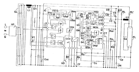
Figure 1 illustrates an electronic ballast for
operating a fluoresenat lamp, if appropriate a plurality
of fluorescent lamps, too, as well as the actual load
circuit with the fluorescent lamp FL. It is known to
connect electronic ballasts to the AC mains, here desig-
nated by L, N, via a radiofrequency filter HF for the
purpose of limiting the radio interference voltage. A
rectifier bridge GL, which supplies as unsmoothed DC
voltage, ie present at the output of the radiofrnqueaey
filter HF. In order to generate a DC voltage which is
above the peak value of the mains voltage, a charging
inductor L1 connected to a charging diode D1 is provided
at the output of the rectifier bridge. The charging
inductor L1 is periodically charged via a first power
transistor V1 which ie likawisn connected to its output.
This first power transistor Vl is controlled by means of
a control loop, which is designed horn, in particular, as
as integrated circuit IC and will be described in more
detail. Put simply, one task of this control loop is
electronic ballasts is to charge the charging inductor L1
to a varying degree as a function of the instantaneous
value of the rectified mains voltage, the control loop
limiting harmonics is the mains current. A second fuac-
tioa is to control the voltage occurring across the
cathode output of the charging diode D1, the so-called
intermediate circuit voltage, to a constant value with a
low degree of fluctuation, in order to obtain load and
mains voltage independence in the electronic ballast.
Furthermore, electronic ballasts usually have a
self-oscillating inverter, with a half-bridge circuit
which is implemented horn by two further power transis
tors V2 and V3 situated in a series circuit connected to
the charging diode D1. The load circuit with at least one
fluorescent lamp FL is coaaectad to the common junction
point of these two further power transistors. In this
exemplary embodiment, there is provided hare for a load
circuit a saturable reactor L2 situated in series with
the fluorescent lamp FL, an ignition capacitor Cz is
connected in parallel with the fluorescent lamp FL.
2,195440
.. s _
Insofar as it is described above, the electronic ballast
,:
according to the invention corresponds to customary
embodiments sad therefore does not seed to be described
is more detail.
R11 the control functions of the electronic
ballast are essentially implemented in the already
mentioned control loop which is designed as as integrated
circuit IC. For the driving of the two further power
transistors V2 and V3, this integrated circuit IC has is
each case a driver circuit HSD sad LSD, respectively,
Which, for their part, are respectively situated at two
mutually inverse autputs of a selection circuit SEL. Is
this case, the driver circuit HSD contains a poteatial-
bridgiag level converter, which changes the drive signal
I5 to the high potential of the power transistor V2. The
said driver circuit has aturn-on input EN to activate
and deactivate it, as will be explained is more detail.
A pulse train is fed to the selection circuit SEL at a
control input Cl, which pulse train controls the
selection circuit in the manner of a flip-flop, with the
special feature that the power transistors V2 and V3
which are activated via the driver circuits HSD sad LSD,
respectively, are driven alternatively but staggered with
respect to one another by a defined dead time. This
controlling pulse train is supplied by a controlled
oscillator CCO, which has three setting inputs to which
are connected a first variable resistor Rf, a second
variable resistor RR and a variable capacitor Cf with
respect to earth - or alternatively with respect to a
defined reference voltage (by way of example, the further
description will always refer to earth here). The
variable resistor RK and the variable capacitor Cf
determine the lower and the upper limiting frequency,
respectively, of the oscillator CCO which is controlled
as a function of current in this example. The prescribed
dead time of the power transistors V2 and Y3 can be set
via the dimensioning of the variable resistor Rf.
The controlling input information for the oscil-
lator CCO which is controlled as a function of current is
X195440
~1
supplied'by the output information from a first opera-
tional amplifier OPR which is low-pass filtered via a
further son-reactive resistor Rc and a further capacitor
Cc.
As will be explained further, a reference voltage
Vref is generated internally in the integrated circuit
IC. The first operational amplifier OPR compares this
reference voltage with a second input voltage, which
corresponds to the mean of the current flowing through
the power transistors V2 and V3 of the half-bridge
circuit. For this purpose, this second input of the
operational amplifier OPR is connected via a series
resistor Ro to the current path of the half-bridge
circuit, that is to say hare the output of the power
transistor V3. This circuit arrangement for controlling
the lamp current flowing in the half-bridge circuit
represents a closed control loop, since the higher this
lamp current rises, the higher the output voltage of the
operational amplifier OPR becomes, too, which output
voltage, on the other hand, controls the controlled
oscillator CCO towards a higher pulse train frequency.
However, this fraqueacy increase effects, for its part.
a reduction in the lamp current. This control loop also
acts in an analogous manner in the opposite direction,
for a decreasing trend of the lamp current. Is steady-
state operation, that is to say whey the fluorescent lamp
is lit without any disturbaacas, this above-described
control loop, is particular with the oscillator con-
trolled as a function of current sad the first opera-
tional amplifier OPR, forms an effective high-frequency
controller for the driving of the half-bridge circuit. To
expand on this, the electronic ballast described here is
also dimmable, since it re possible to control the output
power of the electronic ballast by means of corresponding
fixing of the reference voltage Vref.
Furthermore, the integrated circuit IC contains
a monitoring arrangement which monitors the state of the
fluorescent lamp FL during a steady-state operation, is
particular controls starting of the lamp sad is also
219540
- g _
activated when faulta.or disturbances occur. To this end,
the integrated circuit IC has a monitoring circuit MON,
Which 1e designed as a threshold value circuit with
threshold values which can be set sad is connected, in
turn, by its signal input via a series resistor Rm to the
output of one power transistor V3 of the half-bridge
circuit. This monitoring circuit MON thus receives a
control signal which corresponds to the instantaneous
lamp current and always effects as output pulse QM from
the monitoring circuit MON as soon as the instantaneously
activated threshold value is reached. The respective
threshold value is net by means of a plurality of
selection signals.
One of these selection signals 84 is generated by
a first comparator COMP, which is designed as a differen
tial voltage amplifier, is connected by its positive
input via a deeoupling diode D2 to the output of the
first operational amplifier OPR and to which the refer
ence voltage Vref is fed via its negative input.
Further selection signals are generated by a
timer PST which is connected on the input side to the
junction point of a first internal current source IT sad
as external charging capacitor CT connected to earth.
This internal current source IT is activated at the start
of a turn-on operation for the fluorescent lamp FI. and
begins to charge the extaraal charging capacitor CT, with
the result that a linearly increasing gigaal voltage cor-
responding to the instantaneous duration of the turn-oa
operation is present across the input of the timer PST.
This signal voltage is compared in the timer PST with
predetermined threshold values. When the respectively
activated threshold value is reached, the timer PST
outputs in each case one of the output signals S1, S2 tad
S3 and thus defines specific time segments which will be
described in more detail. The first sad the third output
signal S1 sad S3, respectively, are each fed to the
monitoring circuit MON in order to set there one of the
predetexmiaed threshold values.
The comparator COMP compares the voltage across
2195440
- 10 -
the external capacitor Ccc, which corresponds during
normal operation to the output voltage of the control
operational amplifier OPR, with a value predetermined by
the reference voltage Vref. If the control operational
amplifier leaves its defined control range - this is
possible, in particular, in the dia~iag state in the
case of multi-lamp applications or alternatively in the
case of lamp defects caused, for example, by aged, high-
resiatance lamp filaments - then this is identified by
the comparator COMP. The latter generates the control
Qigaal S4 which is used to set is the monitoring circuit
MON a state in which all the reference levels Mp, Mi sad
Mo are considerably reduced. The monitoring circuit MON
then operates, therefore, satisfactorily even at rela
tivnly low lamp currents.
The second output signal S2 of the timer PST
forms a preparation signal for a disconnection circuit
SD, which is designed as a logic circuit sad performs the
function of shutting dower, if appropriate, the half-
. bridge circuit with the further power transistors V2, V3
- in the event of a disturbance, for example in the event
of a lamp fault. In order to realize this, a control
input of the disconnection circuit SD is connected to the
output of the monitoring circuit MON. An output of the
disconnection circuit SD is connected, later alia, to the
turn-on input EN of the selection circuit SEL, is order
to enable or reset the latter.
Furthermore, there is provided in the integrated
circuit IC a second internal current source ISC, the out
put of which is connected to the junction point between
the non-reactive resistor Rc sad the capacitor Cc of the
external low-pass filter. This second internal current
source ISC has a set input S and a reset input R. The sat
input S is connected to the output of the monitoring
circuit MON, whereas the reset input R is connected to
the output of the selection circuit SEL for the driver
circuits HSD and LSD of the power transistors V2 sad V3,
respectively, of the half-bridge circuit. This second
internal current source ISC is set by an output pulse
z~9~~4a
_ 11 -
from the monitoring circuit,MON sad charges the external
capacitor Cc of the low-pass filter Rc, Cc. Since the
oscillator CCO which is controlled as a function of
current is likewise connected by its control input to
this output of the second internal current source ISC,
the input current coanacted to the said oscillator
increases, with the result that its output pulse train
frequency is increased. As soon as the selection circuit
SEL in one of its two mutually inverse switching states
then activates the driver circuit HSD which is assigned
to that power transistor V2 of the half-bridge circuit
which has a high voltage across it, the second internal
current source ISC is reset by the same output signal
from the selection circuit SEL. In this way, a further
closed control loop is given, which controls the lamp
current cycle by cycle to the respectively prescribed
value which is defined by the iastaataneouely activated
threshold value of the monitoring circuit MON. This
second control loop is auperordinate to the current
controller described in the introduction for steady-state
operation sad limits sad controls the lamp current during
starting of the lamp as well as is the event of detected
cases of disturbances.
A defined power supply of the integrated circuit
IC is achieved by a number of circuit measures. In parti
cular, a turn-on comparator DVLO is provided for the
connection operation, the input of which comparator is
connected, for example, directly to the rectifier bridge
GL via a further series resistor and is connected to
earth via a further charging capacitor Ccc. A supply
voltage Vcc is fed to the iategratad circuit IC at this
input of the turn-oa comparator UVLO. Another possible
way of feeding the supply voltage Vcc to the integrated
circuit IC is illustrated is Figure 1, which uses series
resistors RL, RL' to make it possible to detect sad
utilize state changes is the load circuit, as will be
explained in more detail. The turn-on comparator UVLO
initially has a high input resistance, is order to
activate the IC function with as few losses as possible.
- 12 -
It is furthermore designed in such a way that it already
responds at voltage valuns.which are as low as possible,
for example of the order of magnitude of not more than
150 V DC is an AC mains voltage supply of 220 V, as soon
as the charging capacitor Ccc has been charged accor-
dingly after the connection of the AC mains voltage L, N.
An internal voltage source RSF, which generates the men-
tioned reference voltage Vref, is thus activated. In
addition, a further internal current source BIAS is
connected to the turn-oa comparator WLO, by mesas of
which current source as intpraal auxiliary voltage
IC-BIAS is generated for the integrated circuit IC. Thnee
measures make it possible to start the integrated cir-
cuit. Reference is made to the possibility of deacti-
vatiag the turn-on comparator WLO not only by means of
disconnecting the mains voltage L, N, but also internally
by mesas of a control input connected to the output of
the disconnection circuit SD; the IC function can con-
sequently be turned off is a defined meaner.
During normal operation, the power supply of the
integrated circuit IC is ensured - in this exemplary
embodiment - by a supply circuit DP, DN, Cp which oper-
ates with virtually no losses and comprises a series
circuit formed by two pumping diodes DP and DN as well as
a further charging capacitor Cp. The latter is connected,
on the one hand, to the junction point of these two
diodes and, on the other head, to the output of the half-
bridge circuit, that is to say the junction point of the
two power transistors V2 and V3. This supply circuit
supplies the supply voltage Vcc for the integrated
circuit IC during normal operation.
A control loop With a further comparator TPR is
provided for keeping this supply voltage Vcc constant,
the said comparstor compares the instantaneous value of
the supply voltage Vcc with an upper and a lower prede-
termined reference value in each case. The output of this
comparator TPR is connected to the control connection of
an electronic switch VD, which is designed here as a
transistor switch and the switching path of which is
2195440
- 13 -
arranged between the,chargi_ng capacitor Cp of the supply
circuit and earth. If the instantaneous value of the
supply voltage Vcc detected by the comparator TPR exceeds
the predatarmiaed upper limit value, the comparator TPR
outputs as output signal which switches on the electronic
switch VD. The latter consequently discharges the
charging capacitor Cp of the supply circuit DN, DP, Cp
until the comparator TRP, which operates as far as
possible without any delay, detects the lower limit value
of the supply voltage Vcc and tunas the electronic switch
VD off again. Therefore, thin is high-low control of the
supply voltage Vcc.
An is shown is a circuit diagram detail according
to Figure 2, the pumping diodes DN, DP of the above
described supply circuit as well as the electronic switch
VD may also ba integrated in the integrated circuit IC.
The circuit function described does not change in the
process.
Finally, an arrangement PFC for controlling the
power factor is additionally implemented in the late-
grated circuit IC. It is completely similar is terms of
configuration to corresponding known controllers for
improving the power factor. Although this function is
necessary in the integrated circuit IC, it is only
referred to here because it is of secondary importance in
the context provided here. This arrangement PFC detects
all the parameters which are necessary for determining
the power factor at the charging inductor L1, which is
also equipped with an auxiliary winding for this purpose,
evaluates them and drives the first power transistor V1
accordingly.
The mode of operation of the circuit arrangement
described with reference to Figure 1 csa beat be
explained is the form of timing diagrams, which am
illustrated is Figures 3 to 5, assuming different operat-
ing states in the load circuit, that is to say particul-
arly at the fluorescent lamp FL.
In this case, the timing diagrams of Figure 3
illustrate a normal starting operation. An soon as the
- 14 -
electronic ballast described is connected to mains
voltage L, N, the turn-oa comparator UVLO detects the
supply voltage Vcc, which is increasing across its input,
and activates the integrated circuit IC as soon as its
tuna-oa threshold has been reached. Thereupon, the
current-dependent oscillator CCO initially starts at a
predetermined lower limiting frequency, which is for
instance 75% of the maximum frequency. Not only the
driver circuits HSD and LSD for the power transistors V2
and V3, respectively, of the half-bridge circuit but also
the second internal current source ISC are made to
operate - as described - by means of the selection
circuit SEL which is activated by the pulse train of the
current-dependent oscillator CCO. The second internal
currant source consequently begins to charge the
capacitor Cc of the low-pass filter Rc, Cc accordingly,
with the result that the described first control loop for
the frequency control of the electronic ballast by means
of the current-dependent oscillator CCO is started. The
first internal current~source IT assigned to the timer
PST also begins to charge the external charging capacitor
CT. As long as the first internal current source IT
controlled by the monitoring circuit MON continues to
charge this external charging capacitor, an initially
linearly increasing voltage is supplied to the input of
the timer PST. With predetermined reference levels of the
timer PST, this input signal forms the time base for the
control of all the functional sequences is the electronic
ballast for different operating conditions.
The timing diagram of Figure 3 will be used first
of all to explain details of the sequence during normal
starting of the lamp. t1 designates the starting instant
at which, is the manner described above, the integrated
circuit IC is made to operate is a defined manger when
the mains voltage is connected. The very top diagram of
Figure 3 shows the voltage which increaaes linearly
across the charging capacitor CT sad is fed to the input
of the timer PST. At a later instant t2, this input
voltage for the timer PST reaches a predetermined lower
219440
- 15 -
reference level, which is designated as preheating level
Pp. The time segment which proceeds from the turn-on
instant t1 up to the later instant t2 forma a preheating
phase Gpt for the electronic ballast. Hence, the instant
t2 designates the instant of the end of this preheating
phase. During this preheating phase, the first selection
signal S1 of the timer PST is reset sad hence the moni-
toring circuit MON' is set at a low threshold value, the
preheating threshold Mp. It thus detects, via the series
resistor Rm connected to its input, the current, which is
is the form of an exponential funetioa, in the half-
bridge circuit comprising the two power transistors V2,
V3. The input signals of the monitoring circuit MON which
are in the form of an exponential function and correspond
to this current is the form of as exponential function
are designated by M sad reproduced is a corresponding
section of the timing diagram of Figure 3. As soon as
these input pulses for the monitoring circuit MON reach
the predetermined preheating threshold Mp in the
preheating phase, the monitoring circuit MON emits is -
each case a short control pulse QM. Each of these control
pulses QM emitted by the monitoring circuit MON causes
the second internal current source ISC to be set sad,
furthermore, the selection circuit SEL, which operates in
the manner of a flip-flop and is used for the driver
circuits HSD and LSD, respectively, of the power traasis-
tora V2, V3 of the half-bridge circuit, to be changed
over. The drive pulses HSG and LSG, respectively, emitted
as a result by the driver circuits HSD and LSD, for the
two power transistors V2 and V3, respectively, am
reproduced in the bottom two timing diagrams is Figure 3.
The timer PST signals the and of the preheating
phase Apt at the instant t2 by changing the switching
state of its first selection signal Sl which is fed to
the monitoring circuit MON. As a result, the said moni
toring circuit is changed over to a second, ,higher
threshold value, the ignition threshold Mi. This increase
in the response threshold of the monitoring circuit MON
causes the current is the half-bridge circuit, which .is
21~54~~
-16-
implemented by the two power transistors V2 and V3, to be
increased to a predetermined and limited value Which is
allows the voltage across the fluorescent lamp FL to rise
to the normal ignition voltage.
Accordingly, the ignition phase of the electronic
ballast begins at the instant t2, which ignition phase
must be concluded, is the case of a normally operating
fluorescent lamp FL, by the time an instant t4 is
reached, otherwise the electronic ballast is automati-
tally disconnected. This maximum predetermined time
segment for the duration of an ignition phase is desig-
nated by Ait in Figure 3.
As is the preheating phase Gpt, the monitoring
circuit MON carries on continuously monitoring the
current flowing in the half-bridge circuit and each time
the input signal M corresponding to the instantaneous
half-bridge current concurs with the instantaneously
activated threshold, now the ignition threshold Mi, the
monitoring circuit emits one of the control pulses QM to
the selection circuit SEL until the fluorescent lamp FL
ignites. This is the case at the instant t3 in the normal
ignition operation illustrated in Figure 3. The moaitor-
iag circuit MON does not emit any further control pulses
QM once the fluorescent lamp FL has ignited, because now
the half-bridge current no longer reaches the high
ignition threshold Mi which is still activated in the
monitoring circuit MON.
In spite of this, however, the external charging
capacitor CT assigned to the timer PST is charged
further, with the result that the input voltage fed to
the timer PST continues to rise. The end of the predeter-
mined maximum ignition phase Ait is reached at the
instant t4. At this instant, the input signal of the
timer passes through another of the predetermined refer-
sate levels, the ignition level Pi. If there were a
fault, that is to say if the fluorescent lamp FL were
reluctant to ignite, there would now have to be initiated
as automatic reset of the electronic ballast. On account
of this, the timer PST generates, starting at this
~~~~~~o
17
instant t4, as a further output signal the second selec-
tion signal S2 which identifies a disconnection phase
Ast. This second selection signal is fad to the discoa-
nactioa circuit SD in order to enable it. However, the
disconnection function is not carried out in the example
according to Figures 3, bncausa the disconnection circuit
SD does not receive any further control pulses QM,
emitted by the monitoring circuit MON, at this instant in
the case of a fluorescent lamp FL which ignites in good
time. Incidentally, the ignition threshold Mi continues
to be activated is the monitoring circuit MON.
Finally, the charging of the external charging
capacitor CT reaches a value corresponding to a third
rafarence level, the reset level Pr of the timer PST, at
as instant t5. As a result of the furthest output signal
S3 of the timer PST, the threshold to be detected is now
lowered to a quiescent threshold Mo in the monitoring
circuit MON, which quiescent threshold lies between the
preheating threshold Mp and the ignition threshold Mi.
Therefore, if a normally igniting fluorescent lamp FL is
- assumed, the monitoring circuit MON continues not to emit
any control pulsar, with the result that the enabled
disconnection function cannot be activated. However, the
discharging of the external charging capacitor CT
assigned to the timer PST is initiated at this instant
t5.
This discharging continues until the input aigaal
of the timer PST has fallen to the ignition level Pi at
the instant t6. As a result, the timer 'PST resets the
second output signal 52 and inhibits the disconnection
circuit SD. In contrast, the quiescent threshold Mo
activated in the monitoring circuit MON remains
unchanged. During the further course of events, the
capacitor charge of the external capacitor CT assigned to
the timer PST is reduced further until the input signal,
derived tharnfrom, of the timer PST reaches a steady
state at a quiescent level Po. Steady-state operation of
a lit fluorescent lamp FL is thus achieved. The normal
operatlag phase corraspoading to this state is designated
219440
- 18 -
by Dot is the timing diagram of Figure 3. In this case,
the timer PST sad the monitoring circuit MON are in a
standby state sad the driving of the power transistors
V2, V3 is controlled solely by means of the first control
loop OPR, CCO.
A first of the possible cases of disturbance is
now illustrated in the timing diagram of Figure 4. It is
assumed here that a disturbance (for example due to the
loss of gas in the case of intact lamp filaments) occurs
during the steady-state operation of the lit fluorescent
lamp FL and the fluorescent lamp FL is extinguished. Let
this be the case at an instant t7. Until this point, the
state and the functioning of the integrated circuit IC
correspond to the above-described case in the normal
operating phase Dot. At this instant, the monitoring
circuit MON detects an input signal M, which is above the
guiescent threshold Mo and corresponds to the iastaa-
taneoua half-bridge current, sad emits a control pulse
QM. As a result, inter alia, the second internal current
source IT is turned on again, that is to say the time
- base - in this case directly for a re-ignition phase Ait
- is started. Alternatively, the current source may also
be turned on again only when a plurality of control
pulses QM are counted in a specific period of time.
The ignition threshold Mi is activated in the
monitoring circuit MON and the monitoring circuit MON
continually emits control pulses QM on account of the
excessive current is the half-bridge circuit. The already
explained operation for the ignition phase Git now
proceeds once more. In this case, however, the fluor-
escent lamp FL does not ignite in good time owing to the
assumed disturbance. The disconnection circuit SD, which
has already bees enabled at the expiry of the ignition
phase Ait by setting the second output signal S2 of the
timer PST, is activated by a further control pulse QM
emitted by the monitoring circuit MON, as is shown in
Figure 3 is the timing diagram designated by SD. In this
case, too, it is possible as an alternative to count a
plurality of events before the disconnection circuit SD
z~ ~~~~~
.. _ 19 _
is activated. The disconnection circuit SD deactivates
the selection circuit SEL and at the same time resets the
turn-on comparator D'VLO. Incidentally, as is further
illustrated in Figure 4, all the functions of the inte-
grated circuit IC which are essential for the lamp
operation am reset into a defined starting state, with
the exception of the disconnection circuit SD. After a
lamp change or after reconnection of the mains voltage L,
N, the alectroaic ballast ,is tl~ea ready for operation
once more.
In contrast, if the disturbance assumed at the
instant t7 had only bees a brief disturbance, then
although the above-described operations initiated at this
instant would have started, they would not have been
effected since, is the case of a disturbance which occurs
only briefly, the monitoring circuit MON dons not supply
any further control pulses QM, which are derived from a
continuous disturbance. In this cash, the control oper-
ations would proceed in the integrated circuit IC as
described, with reference to Figure 3, after the ignition
of the fluorescent lamp FL.
In contrast to a normal ignition operation in
accordance with the timing diagram of Figure 3, the basis
of Figure 5 is the case of a fluorescent lamp FL which
does not ignite properly, is the case of which although
there is so filament fault, it is nevertheless perma-
nently reluctant to ignite, for example on account of
lose of gas. In this case, the fluorescent lamp FL does
sot ignite right up to the expiry of the maximum prede-
termined ignition phase Ait. As a result, the discon-
nection circuit SD is enabled by the second selection
signal S2 of the timer PST, the monitoring circuit MON
detects further ignition attempts with excessive half-
bridge current sad emits further control pulses QM. As a
result, the disconnection circuit SD is activated sad
shuts down the electronic ballast, se described above for
a continuous operation disturbance. In this case, too,
the disconnection is maintained until the mains voltage
L, N is disconnected or the fluorescent lamp FL is
219~44Q
- no -
changed.
However, account must also be taken of the fact
that the filament resistance is greatly increased is the
case of as aged fluorescent lamp FL and therefore it does
not ignite normally. In this case, the starting operation
proceeds up to the end of the preheating phase Opt just
like a normally igniting fluorescent lamp FL (Figure 3)
or alternatively like the fluorescent lamp FL which is
reluctant to ignite on account of loss of gas (Figure 5).
However, is contradistinction to the fault case illus-
trated in Figure 5, the superordinate mesa current
control, which is effective by means of the driving of
the first power transistor V1, begins in the event of as
impermissibly increased filament resistance. The mean
current control limits the half-bridge current. As a
coasequencn, the monitoring circuit MON does not generate
nay control pulses QM in the automatically initiated
ignition phase Ait, because its input pulses M derived
from the instantaneous half-bridge current do not reach
the ignition threshold Mi. At the end of the ignition
phase fit, although the disconnection circuit SD is then
enabled once more, it cannot be activated because the
monitoring circuit MON, which is still sat at the igni-
tion threshold Mi, does not generate any control pulses
QM. As the time base progresses, the timer PST then
detects an input signal corresponding to its third
threshold value, the reset threshold value Pr. At this
instant, se is the case of a normal starting operation
(Figure 3), the reference level of the monitoring circuit
MON is lowered to the quiescnat threshold Mo, sad the
discharging of the external charging capacitor CT
assigned to the timer PST is initiated. In this fault
case of a used filament of the fluorescent lamp FL,
although the half-bridge current is limited by the mean
currnat control, it is now sufficient to permit the
monitoring circuit MON to emit control pulses QM. Since
the disconnection circuit SD is still enabled, it is thus
activated and the described diaconnactioa function is
thus started. As~described above, the electronic ballast
~~~~~d~
- 21 -
is shut down, the disconnection being maintained until
the mains voltage L,JN is disconnected or the fluorescent
lamp FL is changed.
The exemplary embodiments described illustrate
that it is possible, by implementing a defined time base
in conjunction with suitable continuous monitoring of the
half-bridge current, to provide automatically proceeding
functional sequences is the electronic ballast which
reliably detect all the conceivably possible operating
states of the fluorescent lamp FL to be operated and put
the electronic ballast into a respectively adapted,
defined state without any manual intervention. These
functional sequences are configured in such a way that
they can be implemented with particular elegance is a
large-scale integrated circuit IC which is resistant to
high voltages. Is this case, sot only is the high
operational reliability of the entire lamp operating
circuit important but also the particularly cost-effec-
tive mass production, because the electronic ballast of
the described type can be implemented using as
intrinsically small number of discrete components.