Note: Descriptions are shown in the official language in which they were submitted.
-
2 1 q54&l~
M~W~l~: ~II~ ~1~1 AND ~.~OD O~' 21aYlJ~ACq~W.ING
8A~, A~D 8~ACB ACt~l!IC ~ Dm~:~
~2N. ~ q~ D~IC ~11 ~ It ~D D ~ o~ DOP
~ rhe present in~ention r-lates ~o a ~et;a~lic
thin-~ilm applied to eleetrodes of vario~s ~cin~s of
~lectronic parts and also relates to a method of
~anuf actu;ring the metallic t~in-rilm.
lt
As a result o~ the rcc:ent advanc~s, th~a size of
various type~ of el~ ic co~.L,~....~nts such as
capacitor~ , coils, ~ilters and oscillator~ ~ave
been reduced. Thi~ has ~ade it ne~essary to prov~d~
lS thln-~ilm el~ctr~ fo~ 8Q co~ponent~ tsuch ~ilms are
typically form~d of aluminum or the li~c-) which exhibit
incre~sed re3istance to electric powe~
crystallinity of such thin-f~ larg~l~r a~S~cts t~eir
resis~ance to electric power. When ~e ~chi~-~ilm
2 0 D~a'csrial i~ polyc~ystalline or amorphous, ato~ns ~i~fuse
~ with~n grain ~oundaries undQr a high currcnt d~nsity or a
higt~ s~r-ss which ~or~ ~oids or hillock~ in the ~ln-
~ilm~ ThcsQ voids or hilloc~es cause ~hor~ ci~cuits or
Ai qçonnec~ion. This pheno~encn L~ re~erred to as
~5 el.- L.oslligrat1 on or ,L~ igration.
~ o avoid t~s proble~, it is necessary to
c~eate mono-crystallin~ s~ru~tures which do nct have t~e
grain boundari~s which ser~Q as di2~usion Pat~S ror th~
atom~. Xowe~erJ it is impo~sible to create such a mono-
cryst~lline struCtur- on a surface of an amorphous body,
a polye~ystalllne body, or an oxientation layer o~ a
2 ~ 9~486
polycrystalline body by con~entional film-forming
~ethods.
The process of t~e present invention provides
~etallic thin-~ilm w~ich is entirely or partially mono-
crys~ ne in struoL~- form~d on the sur~ace of a
SU~G~ ~ body which has an amorphou~ o~ a polycrystalline
stru~ture, or whio~ has a polycrystal~ine orientation
layer, and a ~od for ma~ufacturing cuc~ m-tallic thin-
~il~s.
In the p~eferred e~odi~-nt, the thin film
electrode is a~ranged Por uso in a ~urface acoustic wave
dQvice which ~etter withstands electric power t~an the
prior a~t de~ices.
I~ acc~dancQ with th~ preferred e~bodiment, a
~etallic thin-film ~f t~e presen~ in~ention has an
entirely or p~rtially ~ono-crystalline st~uct~r~, and is
for~ed on t~e surfaco of an a~orphous body, a
polycrystall~n- body, or an o~ienta~ion layer of a
2~ polycrysta~lin~ ~ody, unde~ thQ influence of a radiated
b~a~ w~ich assis~s ths fil~ formati~n onto t~Q surface ~f
t~ a~oxphous body, t~e polycrystallin- body, or the
orientation layer.
Pref ~rably, at least one type of ian selected
2~ ~o~ the group consisting of arqon, heli~, neon,
k~ypton, and xenon io~s, or a ~ixture thereof is used for
the ir~adiating ion beam. ~he metallic thin-film is
pre~erably c~osed of aluminum, gold, silver, copper,
platinu~, titanium, c~ro~iu~ n~kol, tungsten, an alloy
thoreo~, or an alloy essent~ally consist~ng o~ at least
one o~ the abo~e ale~ents.
_ 3 _ 2 1 9 ~ 4 ~ ~
According to one aspect of the present
invention, there is provided ~ thin f~l~ electrode for
us- in a surf ace acoustic wav~ device and a surface
acoustic wave device co~prising an a~orphous layer ~ormed
on a piezoelectric su~strate, and at least one of ~
s~ngle crystal làyer and an oriented layer formed cn the
amorph~us layer.
According to anoth-r asp~ct of the present
invention, there is provided ~ ~ethod o~ fo~ing a
sur~ace acoustic wav~ de~ice h~vin~ a thin ~ le~trode
formed thcreon, the method comprisin~ the steps of
~orming an amorphous layer on a surfac- of a
pi-zo~lectric su~st~ate ~ilo irradiat~ng t~ su~acq of
ehe piezoelectric substratc wit~ an ion beam, and
~5 thereafter forminq at least one o~ a single crystal laye~
and an orie~ted lay~r on a surface o~ the amorphous layer
with ~e assist ~on bea~.
For the ~ 6~e of illustratl~g the inven~ion,
there i5 shown in t~e drawing a plu~ality of forms whic}~
are presently pre~erred, it b-ing undQ~stood, h~we~er,
that the invcntion is not limited to th~ preciso
arrange~ent and instru~entalities shown.
Fig. 1 is a diag~am of an apparatus for
~5 mdnu~ac~uring~ metallic thin-fil~ns, which ap~?aratus
illustr-te~ an e~odi~ent or a meeall~c tnin-~il~ and a
mst~od o~ Dlanufact~ring the ~ilm incorporatod in t~e
present invention; arld
Fig. 2 i~ a sectional diagr~m o~ a sin~le-
crystalliz~ ~etallic thin-~ilm formed on the surface of
an amorphous body.
_ 4 _ ~ ~ 95 4 ~ 6
F~. 3 is a cxoss-sectional vie~ o~ the thin
~il~ electrode, inc~uding a single cry~tal structu~e or
an o~ientation layer st~ucture, which i5 formed on t~e
surface of the piezoelectric sub~trate.
T~e present in~ention will ~e ~otter understood
f~o~ ~he ~ollowlng descrip~ion of the prefersed
e~bodim~nt of a metal}ic thi~-fil~ and a ~et~od o~
1~ ~a~ufacturin~ the fil~ taXen in con~un~tion with ~he
~ccv~anying drawlngs. According to the a ~irst
e~ho~i ent o~ the pr~sent i~vent~on, a (111) orien~ated
alu~inu~ thin-fil3 is ~or~ed on a gl~ss substrat~ 12.
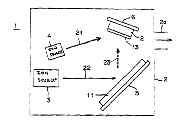
~ig. 1 show~ a dual ion-bea~ s~utterin~
apparatus ~ for for~ing a fil~ on the glass substrate 12.
T~ dual ion-beam sputterin~ app~ratus 1 i~cl~des a
~¢uu~ ch~ ~ 2 and a vac~um pu~p ~not s~own in the
~igure) connected to an exhaust po~t 2~ pro~ided in t~e
right wall of ths v~cuum chamber 2~ Insid~ ~ha vacuum
chambe~ 2, an ion s~urce ~ for sputtering and an ion
sourc~ 4~for a~sisting the fil~ ror~ation a~e positioned
on th- left side, and a backi~g plat~ 5 and a sub~t~ate
s~ L 6, wh~c~ is located a~ov~ th~ bac~ing plate S are
positioned on the rig~t sid-.
2S A thin-fil~ is depo~i~ed u~ng th~ sputtering
apparatus ~ as foll~ws. An alu~inu~ t~xg-t 11, which
acts as a sputtoring ~aterial, is fiX~d ta th~ ~urfac~ of
the ~Xing plate 5 usin~ a ~razing ~ er ~etal such as
indium. A glass substrat~ 12 (i.Q., o~ an a~orphous
material) is fixe~ onto the surfac~ of the substrate
~u~r- ~. Air in the ~acuum ~ 2 i5 ev~cuated to
preferably 0.1 Pa or les~ f~om ~he exnaust port 2a using
21 q54S~
- s ~
th~ vacuu~ pump. If ~he vacuU~ exceeds 0.1 Pa, 'che
resulti~g t~in-f ilm ~rill contain residual gases, such as
~zO~ ~n this ~mbodiment:, the vacuu~ ~ha~sr 2 is
ma~nt~ine~ at 5 x 10'3 Pa.
A ~o-called "ion ass~s~ing" process is
conducted ~y raaiating an ~on ~ean 21 which assists ~e
for~ation or a thin ~ilDt onto the surface o~ ~he s~lass
subst~ate 12, and is continued un~i~ the completion of
the ~or~ation of the f il~. The ~ref erre~ energy f or the
ion bea~ 21 is ~rom lCO eV to 1 ~eV. If the energy is
less than lOo eV, su~ficient energy cannot bQ provided
for the atoms in th~ thin-fil~ 13, while enRrgy aboYe 1
~e-t is ~x~ ngly high so that th~ ion beam 21
disadvantageously sputters and ~i s~nrs~s thc atoms in the
1~ thin-rilm 13 deposited o~ the surface o~ ~e glass
su~stra~e 12, t~u preventing t~ thin-f i lm from growin~ .
The pr~ferr-d c~rrent density o~ the ~ on beam
21 is 0. 01 to 2~ c~2. ~f the cu~rsnt density is less
t~an 0 . 01 mA~ , suf~ic~en~ energy cannot be provided
for t;he ato~ in t~e thin-fil~ 13, whi~ a curren~
density above 20 ~ is exceedingly hiyh so that 'ch~
ion bea~ 21 disad~rantag~ously sputters and disperses the
ato~s in the ~hin-f iln~ 13 deposited or~ surface o~ the
glass substrate 12, ~chus pr~v~nting t~e t~in-~il~ from
2s gro~ing. The incident angle cf t~e iot~ bea3~ 21 to the
gl~ss substra'ce la is preferably set within a range o~
fror~ a- to 4~o witl~ respect to a l~ne which iY normal to
the surfac- of t~e glass substrate 12. If ~e incident
angle do-s not fall witnin the abo~e an~le rang~, it
3o bec~me~ dif~seult to e~fici~n~ly pro~ride energy ~or the
atom~ in ~he thin~ m 13.
An argon ion-~ea~ is pre~-rably radiated onto
~e aluminu~ ~arg~-t 11 from the ion source 3 for
- 6 - 2 1 ~ 5 4 ~ 6
sputtering. The argon ~ons collide with the alu~in~m
target 11 to disperse ions 23 the~fro~. These ~ons 23
reach thQ sur~ace of t~e glas~ su~strate 12 and arQ
depo~ited thereon to form an aluminu~ thin-film 13. The
fil~-20rming speed is preferably 0.~01 nmfsec or more~
When the sp~ed is l-ss than 0.~01 nmlsec, the atoms in
t~e thin-~il~ 13 ~ggrega~e, resulting in grain g~ow~h.
In the present embodi~e~, r~ lm-forming is c~nducted at
O.06 nm~sec and at 25-C. Since the glass subs~rate 12 is
~ade o~ an a~orphous mat~rial, the alu~inu~ thin-film 13
does not have a mono~ alline at~ structure in the
ini~ial stage of thc ~iln form~tion. Howe~er, the
influence o~ th~ glass su~trate 12 di~app~ars and the
thin-film ~3 can attain a ~ono-crystalline ato~ie
lS struc~ure when ~vQral atomic layers have been depo~ited.
After f~ for~ing, t~e glass su~st~ate ~2 is re~ove~
from the vacuum chambor 2. ThQ sur~aco of th~ aluminum
thin-f ilm 13 deposited on the surface of the substrate 12
~ay form an ~xidized layQr 13a by cont~ct with an oxygen
atmospher-, a~ is s~own in F~g. 2.
~he res~ltin~ alu~inu~ thin-film ~3 ~as
con~i~mQd to have a mo~ r ystalline structu~e based on
eva~uation acco~ding to ~h- Rheed ~ethod. Therefore, t~e
grain-boundary diff~sion o~ atoms undsr high cu~rent-
2S densi~y or h~h stress is pr~venta~le by employing the
alu~inun thin-~il~ 13, resultin~ in a relia~le electrode.
For example, thQ ~esistance o~ ~he al~minum thin-film 13
t~ el~atric powcr is approxi~at~ly 100 tLmes tha~ o~ a
polycrystalline ~l~inum thin-fll~.
T~ aluminum thin-f il3 13 has a small degxee o~
lattlce de~eces and exhibit~ excel~ent cor~oS~on
resistance such that t~e number or cor~od-~ portions
decrea~es to approxi~ate~y one tenth t~at of a
-
- ? - ~ 1 9 5 4 P, 6
poly~ tallin~ alu~inum ~in-~ilm. T~us, in addi~ion to
tha usage a:~ an ele~ ~e ~naterial, ~che thir.~ a of the
present in~ren~ion can be advan~ sly employed as, for
example, a thin-fil~ ~aterial for orn~ental articles
S such as ~ir~ors and a ~hin-film material used in a
chloricle at~osphere such as on th~ soaE;hore or in '~he
sea .
A metallic t~in-~il~ and a ~ethod o~
m~nufacturing t~e f ilm i..co~ ated in th~ p~e8erlt
invention may be e~odied in o~her 3peci~ic ~or~s wit~out
d~pa~ting ~ro~ the spirit or es~ential cl~aracteristics
thereof . 'rhe pre~ent e~nbodiment is ~h~r~f ore to ~Q
ccnsidered in al 1 re~pects as illustrati~e and not
s ~a3 ~ ic~
Besides t~e argon ions, heliu~, neon, krypton,
or xenon ion~ may }~B employed alon~ or in oo~bination ~or
th~ ~on be~m 21 for assis~ing tl~ film ~ormation. GOld,
sil~.rer, ~opper, platinu~, ~itanlu~, cl~ um, nickel,
tungsten, an alloy ~ereof, or an alloy e~;sentially
2 0 consist~.ng oS a~ least one c~ the abo~re elements ~ay be
e~ployed ag the thin-f ilr~ ~ateri~ n ~dditlon to
aluminu~. Add~tionally, e~e sputter~ng conditions vary
according to the co~in~tion of th~ t,hin-film ~aterial
and an a~o~ho~s body or t~e tllin-fil~ m2~teri;~1 and a
2 5 poly~ t,~lline body or an orientation layer o~ a
poly~ sl.alline boa~.
Althotagh a ~111) oriented alw~linusn tl~in-film is
formed on a glass ~ubstrate in t~e a~r~ en~hoA;~rtt, the
orienta'cion di~ectlon of th~ thin-fil~ is optional and,
rOr ~xa~ple, a ~200) orient~d alu~inuD- ~in-fil~ ~ay be
fo2~. A boron nitride substrate or ~e liX-- may b~
used b-2~ides thc glass substrat~ th~r, tho thin-f i lra
o~ the pr-s-nt i~v~ntion may b~ ~or~d on a thin-f i 1~
-- 8 -- ? i 9 J 4 ~ S
i~s~tead Or thH substrE~te. It is not nececcAry t:~:at ~e
subst~t~ on wh~ch th~ thin-~il~ is formed i8 entirely
amo~phous, a~ long as ~he surface ther-o~ is amorphous.
MG~C~er~ t~e ~u~strate ~ay be a polycrystalline body o~
s co~prl~e ~n orien~ation layer. As a ~il3-for~in~ method,
~v~por~ion, chemi~al v por deposition, ~olecular ~eam
epitaxy, laser ablation~ or th~ e m~y be e~ployed in
addition to sputterin~. Furthermo~e, t~e ~etallic thin-
fil~ is not reguired to ~e entirely ~ono-crystalline in
struc~re, aa long as it ~s partially ~ono-crystalline in
st~ucture.
~Second Embodiment)
~ thin fil~ ~lQctrodo ~o~ use in a surface
acoustic ~ava d~vics, a surfac~ acoustic wave d~ice, and
a method o~ forming the thin ~il~ electrode and the
surface acoustic wa~e deYice which ~present an
embodlment of the pr~sent invention ~ill be descri~ed.
he ~i~ent will b- perfor~ed vith respect to a case
of for~ing a ~111)-ox~iented alu~in;ua ~in fil~ Oh a
O lithiu~ tantalate substrate in t~Q ~a~oe ~ethcd and
conditions a- in t:he f ir*~ ~odiment .
' Fig. 3 sho~ a cross-sectiona~. vi~ o~ a thin
~il~ el c~Lodo 24 o~ a 6urface acoust~ c waYe devi~e
acco~d~ng to tho preser~t inv-nti~n. T~e thin fil~
2S elQctrode 24 i~ fon~e~, for exasoplo, a~ a p~anar cc~liXe
ID~ t interdigital transduce~) elect~od~ by sp~ttcrin~ on
th- surb~trate on which ~as~ing wa~ per~or~cd o~ by
etc~ the thin ~il~ el~ o~e w~ich was ~ormHd on the
entire su~faee o~ the substrat~.
At an lnitia~ s~age o~ ~ho formatio~ o~
aluminum t~in ~ilm 24, under the influence o~ t~ ion
assis~, th~n ~ 24 ~orm~ 2n ah.o~:~hous l~yer 24a as
s~own in Pig . 3 . ~s th- f ilsll formation PL G~ ses
-
~ ~ i 954~
~urth~r, thin fil~ 24 ~or~ a mono-cry~tallin~ la~er (or
hig~ly-o~iented ~a~er) 24b. A~t~r the t~in film
~ormation, ~hen t~ su~strat~ 23 havlng alu~inum thin
film Z4 ~or~ed on its sub~trate is taken out o~ the
vaCuU~ chamber 2, an oxid~ lay-r 24c is formed in the
surf-ce ~f the a}u~nu~ thin film 24 b~ough~ in contact
wi~h air.
As described abo~e, ~ccordinq to tho present
invention, ~n entirely or ~artial~y ~ono-c~ystallinQ
~allic thin-~il~ is formed on th~ sur~a~e o~ an
amo~phou~ body, a polycrys~iline body, or an or~entation
layer Of d polycrystall~n~ body, whiio radiating an ion
bea~ for a~isting t~e fil~ ~or~ation on~o ~ surface of
the amorphous body, ths ~olyc~ystallino body, or the
lS orient~tion lay~r. Since the ~e~ultin~ ~tallic thin-
film co~tain~ a ~ono ~ alli~Q structu~, t~Q grain-
~oundary diffusion o~ atoms u~der ~igh cur~ent density o~
high st~eas i~ preventable. rurthermo~e, tho metallic
thin-fil~ ~as a small dogree o~ lattic- defects and
zo exhibits excel~en~ c~Losion resistancQ~ Thus, a
xeliablQ ~lectrode can ~ obt~n~ by u8 ~n~ the ~etallic
thin~