Note: Descriptions are shown in the official language in which they were submitted.
3~
;
CUNN~;ULU~ FIXING CUN51~UUL1ON
BACRG~OUND OF THE IN~'ENTION
This invention relates to a construction of fixing a
connector through which signals are fed to and from a printed
circuit board and through which electric power is supplied to
the printed circuit board, and more:particularly to a connector
fixing construction suited for a ~unction block in which a
printed circuit board is connected integrally to a board having
bus bars and connectors, and the printed circuit board and the
board are covered with a cover.
Usually, many electronic devices for effecting various
controls are mounted on an automobile or the like, and
therefore many connectors have been used to connect the
electronic devices to wire harnesses and to connect the wire
harnesses together. Also, there has been used a ~unction block
in which the electronic devices and the connectors are mounted
in a generally concentrated manner to provide a unitary
construction .
A connector fixing construction of a conventional
junction block (hereinafter referred to merely as "JB" ) will
now be described with reference to Figs. 9 through 13. As
shown in Figs. ~ and 10, in the JB 41, a printed circuit board
t hereinaf ter ref erred to merely as ~ PCB " ) 4 2 is f ixedly mounted
on a board 44 through spacers 43. Connectors 45 and various
-- 1 --
.
21gS~O
parts P including resistors, capacitors and shielded coils, are
mounted on the PCB 4 2 .
Various parts P are mounted on the board 44, and bus
bars 47 and 48 and so on are also mounted on the board 44.
Although only part of the bus bar 4 7 is shown in Fig . 10, ends
of the bus bar 47 serve as external connection terminals for a
fuse cavity 49 when the JB 41 is assembled. Ends of the bus
bar 48 serve as external connectLon t~rmin;~l~ for connectors 51
when the JB 41 is assembled.
When the JB 41 is assembled as shown in Fig. 9, the
upper sides of the PCB 42 and the board 44 are entirely covered
with a cover 52 of a synthetic resin while the lower sides
thereo~ are covered with a cover 53. A fitting side of each
connector 45 is disposed generally flush with an opening formed
through an upper wall of the cover 52, and hence is exposed to
the exterior through this opening. The fuse cavity 49 and the
connectors 51 are pro~ected from the upper surface of the cover
52 .
The internal structure of the JB 41 will be described
with reference to Figs. 11 and 12. Fig. 11 is a cross-
sectional view taken along the line A-A of Fig. 9, and Fig. 12
is an enlarged, cross-sectional view of an important portion of
Fig. 11.
As shown in Fig. 11, a bus bar 54, extended t~lrough the
board 44, is connected at one end to a circuit pattern 46, and
-- 2 --
21g58~ -
the other end of the bus bar 54 is electrlcally connected to
the bus bar 47 and so on through a conductive member 55. As
shown Ln Fig. 12, the circuit pattern 46 is formed on a lower
surface of the PCB 42, and ~rminAl~ of the various parts P and
t~rminAl~ 45a of the connectors 45 are soldered to the circuit
pattern 4 6 .
As shown in Fig. 12, the connectors 45, the PCB 42 and
the cover 52 are arranged such that the ~PrminAls 45a of each
connector 45 extend through the PCB 42, and are soldered at
their distal ends to the circuit pattern 46. The connector 45
is fixedly secured or fastened at its central portion to the
PCB 42 by a screw 56. A large gap G is formed between the
peripheral edge of the opening, formed through the cover 52,
and the peripheral surface of the connector 45, and the two are
normally out of contact with each other.
When connecting the connector 45 to a mating connector
(not shown), the mating connector is inserted at its front end
into the fitting side of the connector 45, and is pushed
downward to be fitted in the connector 45. When removing or
withdrawing the mating connector from the connector 45, the
mating connector is pulled upwardly to be withdrawn from the
connector 45.
However, in order to prevent incomplete contact and so
on, t~rminAl~ of the mating connector are press-connected
respectively to the terminals of the connector 45, and
-- 3 --
~ 219~30
.. .
.
therefore a suitable degree of frictional resistance develops
therebetween, and therefore the mating connector can not be
easily connected to and removed from the connector 45 merely by
urging the mating connector downwardly and upwardly, and
particularly when removing the mating connector, in some cases,
it is forcibly swung to be withdrawn from the connector 45.
More specifically, as shown in Fig. 12, when
withdrawing the mating connector from the connector 45, the
connector 45 is forcibly swung in directions indicated by
arrows B since the large gap G is formed between the connector
45 and the peripheral edge of the opening in the cover 52. As
a result, a load is applied to the area of soldering between
the ~-~rm; n~ 1 s 45a and the circuit pattern 46, so that the
solder portions may be cracked. If this occurs, the connectLon
between the terminals 45a and the circuit pattern 46 becomes
incomplete, so that the proper circuit operation fails to be
carried out
Further, as shown in Fig. 13, when connecting the
mating connector to the connector 45 by pushing the former into
the latter, the PCB 42 is deformed from a horizontal condition
(indicated in phantom) into an arcuate or curved condition
indicated in solid lines. When withdrawing the mating connector
from the connector 45, the PCB 42 is deformed upwardly from the
position (indicated in phantom) into an arcuate condition. As
a result, a load is applied to the solder portions when
-- 4
21~5~3~
inserting and removing the mating connector, so that the above-
mentioned problems have been encountered.
SUMMARY OF THE INVENTION
It is an object of this invention to provide a
connector f ixing construction in which when connecting and
disconnecting a mating connector relative to a connector
mounted on a printed circuit board, solder portions are
prevented f rom being cracked .
The above ob~ect of the invention has been achieved by
connector fixing constructions mentioned in the following
paragraphs ( 1 ) to ( 5 ):
(1) A connector fixing construction comprising a
connector mounted on a printed circuit board, and a cover
coverlng the printed circuit board, the cover havLng an opening
through which a f itting side of the connector ls exposed;
characterized in that a wall portion extends downwardly from
that portion of the cover defining a peripheral edge portion of
the opening, and surrounds a peripheral surface of the
connector.
In this connector fixing construction, the wall portion
extends downwardly in surrounding relation to the peripheral
surface of the connector, and therefore even if a lateral
external force acts on the connector when the mating connector
is inserted into and removed from the connector, the wall
-- 5
21~S8~
portion prevents the connector from moving, so that damage to
solder portLons is certainly prevented.
( 2 ) In the connector f ixing construction according
to the above paragraph ( 1 ), there is provided a support member
having a support portion of a convex configuration disposed in
close proximity to a predetermined portion of a soldering
surface of the printed circuit board facing away from a part-
mounting surface thereof having the connector mounted thereon.
In this connector fixing constructlon, there is
provided the support member having the support portion of a
convex configuration disposed in close proximity to the
soldering surface of the printed circuit board facing away from
the part-mounting surface thereof having the connector mounted
thereon. Therefore, even if the printed cLrcuit board is urged
or pressed downward when the mating connector is inserted into
the connector, the printed circuit board is abutted against the
support portion, and is positively prevented from being flexed
or def ormed downwardly .
( 3 ) In the connector fixing construction according
to the above paragraph ( 1 ), the wall portion, formed on the
cover, is extended to a position close to the printed clrcuit
board .
In this connector fixing construction, the wall
portion, formed on the cover, is extended to the position close
to the printed circuit board. Therefore, the wall portion
-- 6
2~9~30
prevents the connector from being laterally moved, and also
positively prevents the printed circuit board from being flexed
or deformed upwardly. Therefore, with this arrangement and
also with the arrangement of the above paragraph (2), damage to
the solder portions i9 more certainly prevented.
(4) In the connector fixing con5truction according
to the above paragraph ( 1 ), holder ribs are formed on an inner
surface of the wall portion, and cover part of an upper surface
of the connector, the holder ribs being provided at such
positions that they will not interfere with a mating connector
when the mating connector is inserted Lnto and removed from the
connector .
In this connector fixing construction, the holder ribs
are formed on the inner surface of the wall portion, and cover
part of the upper surface of the connector, the holder ribs
being provided at such positions that they will not interfere
with the mating connector when the mating connector is inserted
into and removed from the connector. Therefore, as in the
connector fixing construction of the above paragraph ( 3 ), the
wall portion prevents the connector from being laterally moved,
and the upward f lexing or def ormation of the printed circuit
board is certainly prevented when wi~hdrawing the mating
connector from the connector. Therefore, with this arrangement
and with the arrangement of the above paragraph ~ 2 ), damage to
the solder portions is more certainly prevented.
-- 7
~ 2~g~8~
(5) In the connector fixing construction according
to the above paragraph (l), a fixing boss is formed on the
connector, and is held against the printed circuit board, and
a screw fixing portion is formed on a lid member covering a
soldering surface of the printed circuit board, and is held
against the soldering surface, and the connector and the lid
member are fastened together by a screw, with the printed
circuit board held therebetween.
In this connector fixing construction, the connector
and the lid member are fastened together by the screw, with the
printed circuit board held therebetween. Therefore, the
printed circuit board will not be flexed or deformed when the
mating connector is inserted into and removed from the
connector, and a load applied to the solder portions, is
reduced, thereby more certainly preventing damage to the solder
portions .
BRIEF DESCRIPTION OF THE DRAWING~
Fig. l is an enlarged cross-sectional view showing an
important portion of a first embodiment of a connector fixing
construction of the present invention;
Fig. 2 is a plan view showing an important portion of
the connector fixing construction of Fig. 1;
Fig. 3 is a cross-sectional view showing a structure
below a printed circuit board of the construction of Fig. 1;
-- 8 -- =
2195~
.
Fig. 4 is an enlarged cross-sectional view of an
important portion in Fig. 3;
Fig. 5 is a plan view of an important portion in Fig.
3;
S Fig. 6 is an enlarged cross-sectional view showing an
important portion of a second embodiment of the invention;
Fig. 7 is a view explanatory of the operation in Fig.
6;
Fig. 8 is an enlarged cross-sectional view showing an
important portion of a third embodiment of the invention;
Fig. 9 is a perspective view of a conventional ~unction
block;
Fig. 10 is a perspective view of a connector fixing
construction in Fig. 9;
Fig. 11 is a cross-sectional view of an important
portion in Fig. 9;
Fig. 12 is an enlarged cross-sectional view of an
important portion in Fig. 11; and
Fig. 13 is a schematic cross-sectional view showing the
flexing or deformation of a printed circuit board.
DETAI:LED DESCRIPTI~N OF T~IE INVENTIQN
A first embodiment of a connector fixing construction
of the present invention will now be described with reference
to Figs. 1 and 2. Figs. 9 to 13, used for the explanation of
g
~ 219~3~
the conventional construction, will be used also in the
description of the embodiments. Fig. l is an enlarged cross-
sectional view showing an important portion of the connector
fixing construction of the invention, and Fig. 2 is a plan view
showing an important portion of the connector fixing
construction .
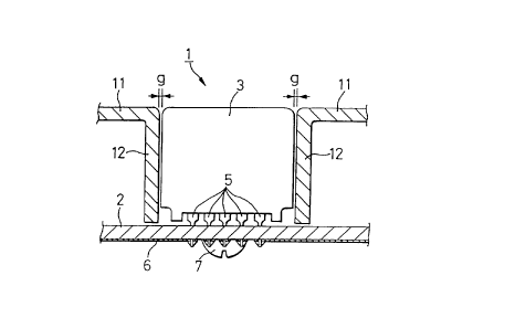
As shown in Fig. l, the connector fixing construction
of this ~mhorl; t comprises a f lat printed circuit board
( PCB ) 2 having a circuit pattern 6 f ormed thereon, connectors
3 each having a plurality of ~rm;nAls 5 soldered to the PCB 2,
and a cover 11 covering the PCB 2 . The ~rm; nA 1 s 5, pro~ecting
from the lower side of the connector 3, extend through the PCB
2, and are connected by soldering to the circuit pattern 6
formed on a soldering surface thereof. The connector 3 is
fastened to the PCB 2 by a screw 7, and the connector 3 is
firmly fixed to the PCB 2 by thLs screw and the solder.
A wall portion 12 extends downwardly from the cover 11
at a peripheral edge portion oi each opening (through which a
fitting side of the associated connector 3 is exposed to the
exterior) formed through the cover ll, to a position close to
the PCB 2, and surrounds a peripheral surface of the connector
3. Namely, as shown in Fig. 2, the wall portion 12 surrounds
the entire periphery of the connector 3. A large insertion gap
Gl for receiving a retaining portion of a mating connector is
form.~ed between the peripheral surface of the connector 3 and
-- 10 --
219~830
the wall portion 12 at part of the periphery of the connector
3. Elowever, only a small gap a is formed between the connector
3 and the wall portion 12 except that region where the
insertion gap G1 is provided.
Operations, effected when connecting and disconnecting
the mating connector relative to the connector 3, will now be
described. As shown in Fig. l, the mating connector is
inserted into the fitting side of the connector 3 from the
upper side, and is connected to the connector 3. At this time,
even if trying to insert the mating connector into the
connector 3 while forcibly swinging the mating connector
laterally since a frictional resistance develops between the
~rrninA~s of the two connectors, the connector 3 is prevented
from being laterally moved since the entire periphery of the
lS connector 3 is surrounded by the wall portion 12. Therefore,
the mating connector is urged only substantially vertically,
and a lateral load will not be applied to the solder portions
by which the terminals 5 are connected to the circuit pattern
6, and therefore damage, such as a crack, to the solder
portions is certainly prevented.
When withdrawing the mating connector from the
connector 3, the connector 3 is prevented from being forcibly
swung laterally since the connecter 3 is surrounded by the wall
portion 12 over the entire periphery thereof; otherwise, this
forcible swinging movement would be effected so as to disengage
-- 11 --
21g~3~
the t~rrnini~lc of the mating connector, press-connected
respectively to the terminals of the connector 3, therefrom.
The wall portion 12 is extended to the position close
to the PCB 2, and therefore the upward deformation or flexing
of the PCB 2 is prevented by the lower end of the wall portion
12 when withdrawing the mating connector from the connector 3.
As a result, even when the mating connector is withdrawn, a
load will not be applied to the solder portions by which the
~rm; ~1 s 5 are connected to the circuit pattern 6, and
therefore damage to the solder portions is certainly prevented.
Next, in the connector f ixing construction of this
embodiment, an arrangement of preventing the flexing of the PCB
when connecting and disconnecting the mating connector relative
to the connector will be described with reference to Figs. 3 to
5. Fig. 3 is a cross-sectional view of the construction of
preventing the f lexing of the PCB when connecting and
disconnecting the mating connector, Fig. 4 is an enlarged
cross-sectional view of an important portion, and Fig. 5 is a
plan view of the portion shown in Fig. 3.
As shown in Fig. 3, a support member 22 is provided
below the PCB 2 through spacers 21. Hollow cylindrical support
portions 23 are formed respectively on those portions of an
upper surface of the support member 22 where the connectors 3
are fastened with the screws 7, each of the cylindrical support
portions 23 surrounding a respective one of the screws 7. The
-- 12 --
2195~30
upper ends of the support portions 23 are disposed in close
proxLmity to the soldering surface of the PCB 2.
The support member 22 is in the form of a flat plate,
and underlies that portion of the PCB 2 having the connectors
3 mounted thereon, over an entire area thereof, within a
junction block (JB) 1, as indicated by a broken line in Fig. 5.
The support portions 23 are formed in surrounding relation
respectively to the screws ~ provided respectively at generally
central portions of the two connectors 3.
The lower ends of each wall portion 12 is extended to
the position close to the PCB 2. Fig. 5 shows those portions
relevant to the connectors 3 within the JB 1, but the wall
portion 12 in an upper block B1 ( Fig . 5 ) is shown in cross-
section for convenience ' sake while a lower block B2 is shown
in a plan view.
When the mating connector is inserted into the
connector 3, the connector 3 is urged downward, and therefore
the PCB 2 is also urged downward. However, since the support
portion 23 is provided in close proximity to the PCB 2, the
soldering surface of the PCB 2 is abutted against the support
portion 23, so that the PCB 2 will not be flexed downward
beyond the support portion 23. As a result, a load will not be
applied to the solder portions by which the terminals 5 of the
connector 3 are connected to the circuit pattern 6, and
therefore damage, such as a crack, to the solder portions is
-- 13 --
~ 21~583~
prevented, thereby enhancing the reliability of the JBl.
Next, the operation of withdrawal of the mating
connector from the connector 3 will be de5crLbed. In the above
embodiment, the support member 22 and the support portions 23
are provided, and besides the wall portions 12 each surrounding
the associated connector 3 are extended to the position close
to the PCB 2. Therefore, when withdrawing the mating connector
from the connector 3, the lower end of the wall portion 12
prevents the PCB 2 from being flexed upward. Therefore, a load
due to the forcible swinging of the connector 3 will not be
applied to the solder portions on the PCB 2, and besides the
upward flexing is prevented. This, together with the provision
of the support portion 23, achieves double protection, and
therefore all of the problems, encountered with the
conventional construction, are overcome.
Next, a second embodiment of a connector fixing
construction of the invention will be described with reference
to Figs. 6 and 7. This embodiment differs from the first
embodiment in that a load will not be applied to the solder
portions, utilizing a cover covering an upper portion of the
connector f ixing construction . Those portions of this
embodiment, performing the same functions as those of the first
embodiment, will be designated by identical reference numerals.
In this embodiment, a wall portion 12 extends
downwardly from the cover 11 at a peripheral edge portion of
-- 14 --
~ 21~5~3~ , _
each opening ( through which a f itting side of an assoclated
connector 3 is exposed to the exterior) formed through a cover
11, to a position close to a PCB 2, and surrounds a peripheral
surface of the connector 3. Namely, the wall portion 12
surrounds the entire periphery of the connector 3. Holder ribs
25 are formed on an inner surface of the wall portion 12, and
cover part of the upper surface of the connector 3. The holder
ribs 25 are provided at such positions that they will not
interfere with a mating connector 35 when the mating connector
35 is inserted into and removed from the connector 3.
Therefore, as in the first embodiment, the wall portion
12 prevents the connector 3 from being moved or swung
laterally, and also the upward flexing of the PCB is certainly
prevented when withdrawing the mating connector 35 from the
connector 3. Therefore, with this arrangement and also with
the arrangement as described above for the first embodiment,
the solder portions are more certainly prevented from damage.
Next, a third embodiment of a connector fixing
construction of the invention will be described with reference
to Fig. 8. This embodiment differs from the first embodiment
in that a load will not be applied to the solder portions,
utilizing a lid member covering a lower portion of the
connector fixing construction. Those portions of this
embodiment, performing the same functions as those of the first
embodiment, will be designated by identical reference numerals.
-- 15 --
~
2195~3~
In this embodiment, a fixing bos5 31 of a predet~rm;n~d
length i8 formed on a lower surface of a connector 3, and
t~rm;n~]s 5 pro~ect from this lower surface. A screw hole 32
(indicated by a broken line) is formed in the fixing boss 31.
S When the tr~rm; n~ l q 5 are soldered to a circuit pattern 6 on a
PC~ 2, a lower end of the fixing boss 31 is held in contact
with an upper surface of the PCB 2.
A lower surface of the PCB 2 is covered with the lid
member 33 so as to prevent dust from adhering to this lower
surface. In this embodiment, screw fixing portions 34 of a
convex shape are formed respectively at those portions of the
lid member 33, corresponding to the fixing bosses 31. The screw
fixing portion 34 has a height corresponding to the distance
between the lid member 33 and the PCB 2, and when the lid
member 33 is fixedly mounted in position, distal ends of the
screw fixing portions 34 are disposed in close proximity to the
lower surface of the PCB 2.
In the above connector fixing construction, when
mounting the connectors 3, each connector 3 is located in a
predetermined position on the PCB 2, and the terminals 5 are
passed through the PCB 2, and are soldered to the circuit
pattern 6 formed on the PCB 2. The amount of extending of the
terminals 5 from- the lower surface of the PCB 2 is determined
by the height of the fixing boss 31 held against the PCB 2.
When the lid member 33 is mounted af ter the terminals 5 are
-- 16 --
~ 2~5~3~
j -- '
soldered to the circuit pattern 6, the f Lxing bosses 31 are
opposed respectively to the screw fixing portions 34 through
the PCB 2.
In this condition, screws 7 are passed respectively
through the screw fixing portion 34 from the lower side, and
are tightened to fix the lid member 33 to the fixing bosses 31.
As a result, the connectors 3, the PCB 2 and the lid member 33
are fastened together.
In this construction, when connecting a mating
connector 35 to the connector 3, force Fa acts on the connector
3. ~owever, since the connector is fixed to the PCB 2, and
also fixed to the lid member 33, a load applied to the solder
portions on the t~rmi n~ l s 5 is reduced. This, together with
the provision of a wall portion 12, prevents the solder
portions from being cracked.
When withdrawing the mating connector 35 from the
connector 3, force Fb acts on the connector 3. In this case,
also, a load applied to the solder portions is reduced since
the connector 3 is fixed to the PCB 2 and also fixed to the lid
member 33. This, together with the provision of the wall
portion 12, prevents the solder portions from being cracked.
The present invention is not to be limited to the above
embodiments, and various modifications can be made. For
example, in the third embodiment, reinforcement ribs may be
formed on the lid member 33 to extend radially from the screw
-- 17 --
,21~3û -
fixing portion 34, or may be provided ln the form of a grid so
as to increase the strength of the lid member 33 to prevent the
flexing or deformation thereof. Bach of the support portions
23 does not always need to be provided ln surroundlng relation
to the screw 7, but may be formed at other position.
As described above, in the connector-fixing
constructions of the invention, the connectors are mounted on
the printed circuit board, and the wall portions, covering the
peripheral surfaces of the connectors, respectively, are formed
on the cover covering the printed circuit board.
Therefore, even if a lateral external force acts on the
connector when the mating connector is inserted into and
removed f rom the connector, the lateral movement of the
connector is prevented by the wall portion. Therefore, a load
is not applied to the solder portions by which the terminals of
the connector are connected to the circuit pattern, and damage,
such as a crack, to the solder portions is prevented, thereby
providing the highly-reliable connector fixing construction.
There is provided the support member having the support
portions of a convex configuration each disposed in close
proximity to the soldering surface of the printed circuit board
facing away from the part-mounting surface thereof having the
connectors mountëd thereon.
Therefore, even if the printed circuit board is urged
or pressed downward when fitting the mating connector into the
- 18 -
830
connector, the printed circuit board is abutted against the
support portion, and is certainly prevented from being flexed
or deformed downward. Therefore, a load 19 not applied to the
solder portions by which the terminals of the connector are
connected to the circuit pattern, and damage, such as a crack,
to the solder portions is prevented.
Each of the wall portions is extended to the position
close to the printed circuit board. Therefore, the lateral
movement of the connector is prevented, and also the upward
flexing or deformation of the printed circuit board is
prevented when withdrawing the mating connector from the
connector. Therefore, this, together with the provision of the
support member, more certainly prevents damage to the solder
portions, and the reliability of a device, to which this
connector fixing construction is applied, is enhanced.
The holder ribs are formed on the inner surface of the
wall portion, and cover part of the upper surface of the
connector, and the holder ribs are provided at such positions
that they will not interfere with the mating connector when the
mating connector Ls inserted into and removed from the
connector. The wall portion prevents the connector from
laterally moving, and also certainly prevents the upward
flexing or deformation of the printed circuit board.
Therefore, this, together with the provision of the support
member, more certainly prevents damage to the solder portions.
-- 19 --
~ 219~3~
The printed circuit board i5 held between each of the
connectors and the lid member, and in this condition each
connector is fastened to the lid member by the screw.
Theref ore, the strength of the printed circuit board is
enhanced, and the printed circuit board will not be flexed or
deformed when the mating connector is inserted into and
withdrawn from the connector, so that a load, applied to the
solder portions, is reduced, thereby more certainly preventing
damage to the solder portions.
-- 20 --