Note: Descriptions are shown in the official language in which they were submitted.
219926
1
A DEMODULATOR FOR RECEIVERS USED FOR COMMUNICATIONS
BACKGROUND OF THE INVENTION
Field of the Invention
The invention relates to a demodulator for receivers used in satellite
communication, mobile communication, or mobile satellite communication.
Description of the Prior Art
A conventional example of such a demodulator is disclosed in an article
entitled
"A New Coherent Demodulation Technique for Land-Mobile Satellite
Communications",
International Mobile Satellite Conference, Ottawa, pp 622 - 627, 1990. The
demodulator comprises a reception portion, a digital quadrature detector, a
receiving
filter and a bit timing estimation circuit. The latter is connected to the
filter and
provides a correction parameter which is used by an interpolation processing
portion to
provide a timing signal. A disadvantage of such a demodulator is that fading
or blockage
of the input signal can result in a prolonged loss of synchronization.
It is an object of the present invention to provide a demodulator in which,
after
a signal which has been lost by fading or blockage has been restored, timing
recovery
circuitry attempts to recover the synchronization again after a relatively
short time, as
compared with known demodulators, so as to re-establish the synchronization
quickly.
SUMMARY OF THE INVENTION
According to one aspect of the present invention, a demodulator comprises a
reception portion for receiving a communication signal including predetermined
information outputted from a modulator; a correction parameter output portion
connected
to the reception portion for outputting a correction parameter based on the
communication signal; a demodulated information output portion connected to
the
reception portion and the correction parameter output portion for outputting
demodulated
information based on the communication signal and the correction parameter; a
detector
for detecting whether the demodulated information includes the predetermined
information, and for outputting a first signal when the predetermined
information is
CA 02195926 2000-O1-20
2
detected and a second signal when the predetermined information is not
detected; and a
storage portion connected to the detector for storing the correction parameter
outputted from
the correction parameter output portion when the first signal is inputted, and
for outputting
a stored correction parameter to the correction parameter output portion when
the second
signal is inputted.
The correction parameter output portion may be connected to the detector and
the
storage portion, the correction parameter output portion then outputting the
correction
parameter inputted from the storage portion when the detector outputs the
second signal, and
outputting the correction parameter based on the communication signal inputted
from the
reception portion when the detector outputs the first signal.
A demodulator of the present invention may further comprise a reset signal
output
portion connected to the detector for outputting a reset signal when the
detector successively
outputs the second signal.
The predetermined information may be an information signal which is
periodically
inserted in the signal outputted from the modulator.
According to a second aspect of the invention, a demodulator of the present
invention
comprises a reception portion for receiving a communication signal outputted
from a
modulator; a correction parameter output portion connected to the reception
portion for
outputting a correction parameter based on the communication signal; a
demodulated
:?0 information output portion connected to the reception portion and the
correction parameter
output portion for outputting demodulated information based on the
communication signal and
the correction parameter, a level signal output portion connected to the
reception portion for
outputting a first signal when a receiving level of the communication signal
is higher than
a threshold level, and outputting a second signal when a receiving level of
the communication
?5 signal is lower than a threshold level; and a storage portion connected to
the level signal
output portion for storing the correction parameter outputted from the
correction parameter
output portion when the first signal is inputted, and for outputting the
stored correction
parameter to the correction parameter output portion when the second signal is
inputted.
The correction parameter may comprise any one of a parameter for controlling
:30 processing timing of communication signal, a parameter for controlling
frequency, a
parameter for controlling a phase of a Garner to correctly determine the data,
and a
parameter for controlling a gain of the pre-amplifier to make the receiving
signal level.
CA 02195926 2000-O1-20
3
According to a third aspect of the invention, there is provided a demodulator
comprising: detection means for detecting whether a predetermined condition is
present in
a communication signal, for outputting a first signal when the predetermined
condition is
present and for outputting a second signal when the predetermined condition is
not present;
and storage means connected to said detection means for storing a correction
parameter when
said detection means outputs the first signal and for outputting the stored
correction
parameter when said detection means outputs the second signal.
According to a fourth aspect of the invention, there is provided a demodulator
comprising: demodulated information generating means for generating
demodulated
information based on a communication signal; detection means, connected to
said
demodulated information generating means, for detecting whether a
predetermined condition
is present in at least one of the communication signal and the demodulated
information, for
outputting a first signal when the predetermined condition is present and for
outputting a
second signal when the predetermined condition is not present; and storage
means, connected
to said detection means, for storing a correction parameter when said
detection means outputs
the first signal and for outputting the stored correction parameter when said
detection means
outputs the second signal.
BRIEF DESCRIPTION OF THE DRAWINGS
Embodiments of the invention will now be described, by way of example only,
with
reference to the accompanying drawings, in which:-
Figure 1 is a schematic block diagram of a first embodiment;
Figure 2 illustrates operation of the first embodiment;
Figure 3 is a schematic block diagram of a second embodiment;
'25 Figure 4 illustrates operation of the second embodiment;
Figure 5 is a schematic block diagram of a third embodiment;
Figure 6 is a schematic block diagram of a fourth embodiment;
Figure 7, labelled PRIOR ART, is a schematic block diagram of a known
conventional demodulator; and
:30 Figure 8, labelled PRIOR ART, illustrates a known interpolation processing
operation.
CA 02195926 2000-O1-20
3a
DETAILED DESCRIPTION OF THE PREFERRED EMBODIMENTS
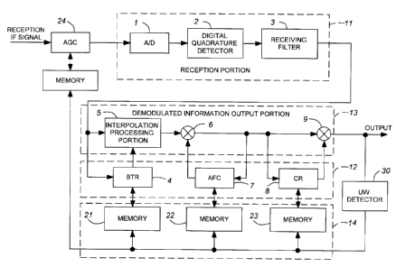
The receiver demodulator shown in Figure 7, and labelled "PRIOR ART" comprises
a reception portion 11, which comprises an analog-to-digital converter
(hereinafter referred
to as "A/D converter"), a digital quadrature detector 2 and a receiving filter
3. An
intermediate frequency signal (hereinafter referred to as "IF signal") is
inputted into the A/D
converter 1. This IF signal is A/D-converted and outputted to the digital
quadrature detector
2 which is connected to the A/D converter 1. The detector 2 receives the
output signal from
the A/D converter 1, and outputs a base band signal comprising an in-phase
component and
a quadrature component according to the input signal.
The receiving filter 3 is connected to the digital quadrature detector 2 to
receive the
base band signal outputted therefrom. This receiving filter 3 shapes its
waveform and
removes out-of-band noise.
A correction parameter output portion 12 comprises a bit timing estimation
circuit 4
(hereinafter referred to as "bit timing recovery (BTR) circuit"), an automatic
frequency
cnntr~l IAFC'.l circuit 7 lhPrPinaftPr rPfPrrPr~ tn ae "AF!'' 7"1 a.,~i a r~,-
,-;Ar ..l,~~o
2195926
4
estimation circuit 8 (hereinafter referred to as "CR 8"). The BTR 4 is
connected to the
receiving filter 3 to receive signals outputted therefrom. The BTR 4 estimates
timing
of decision (hereinafter referred to as Nyquist point) according to the input
signal, and
outputs its result as a correction parameter.
A demodulated information output portion 13 comprises an interpolation
processing portion 5, a first multiplier 6, and a second multiplier 9. The
interpolation
processing portion 5 is connected to the receiving filter 3 and BTR 4,
receives signals
output from both, and generates a signal at a timing of the Nyquist point from
the signal
outputted from the receiving filter 3, according to the signal outputted from
BTR 4.
The inputs of first multiplier 6 are connected to the interpolation processing
portion 5 and AFC 7, respectively. It receives the signals outputted from the
interpolation processing portion 5 and the AFC 7, and removes signal
components
outputted from the AFC 7 from the signal outputted from the interpolation
processing
portion 5.
AFC 7 interconnects the output and a second input of the first multiplier 6.
It
receives the signal outputted from the first multiplier 6, estimates the
frequency deviation
of the input signal, and outputs a signal based on this frequency deviation as
a second
correction parameter.
The input of CR 8 is connected to the output of the first multiplier 6. It
receives
the signal outputted from the first multiplier 6, estimates phase difference
based on the
input signal, and outputs a signal based on this phase difference, as a third
correction
parameter to second multiplier 9.
This second multiplier 9 has a first input connected to the output of the
first
multiplier 6 and the input of the CR 8, in common, and a second input
connected to the
output of CR 8. It receives the signals outputted from the first multiplier 6
and the CR
8, rotates the signal outputted from the first multiplier 6 in accordance with
the signal
from the CR 8, and performs coherent detection.
The operation of the demodulator shown in Figure 7 will now be explained. The
reception IF signal from the modulator is inputted into A/D converter l, and
is A/D
converted. The signal outputted from the A/D converter 1 is inputted into the
digital
quadrature detector 2 which outputs signals as an in-phase component and a
quadrature
component according to input signal.
219592
The digital quadrature detector 2 converts the input signal into an in-phase
component I~ (nT) of the base band signal and a quadrature component QQ~ (nT)
of the
base band signal and outputs them. During this process, quasi-coherent
detection is
performed on the output signal.
5 An output signal from the digital quadrature detector 2 is obtained in
accordance
with the following formulae (1):-
I~ = I(nT) cos (OWnT+8) - Q(nT) sin (OwnT+B)
Q~(nT) = Q (nT) cos (~wnT+B) + I (nT) sin (Oc~nT + e) (1)
where I (nT) represents the in-phase component of the signal outputted from
the
modulator, and Q (nT) represents the quadrature component of the signal
outputted from
the modulator.
T represents the sampling period for generating the in-phase component signal
and the quadrature component signal which are outputted from the digital
quadrature
detector 2. Normally this sampling period T is included in the received
signal, and it
is set to approximately 1/4 of the Symbol period.
The sampling period T is not synchronized with the Symbol period of the
received signal, and the sampled data does not necessarily include the data
sampled at
the Nyquist point.
Ocu represents a frequency deviation of the received signal. In addition, 8
represents an initial phase difference between the received signal and the
oscillator
included in the digital quadrature detector 2. n indicates an n-th sample time
during the
period T.
The base band signal which is outputted from the digital quadrature detector 2
is
inputted into the receiving filter 3. The receiving filter 3 shapes waveform
and removes
the out-of band noise. The signal outputted from receiving filter 3 is
inputted into BTR
4, which estimates the timing of the Nyquist point (*) according to the input
signal.
The signals outputted from the receiving filter 3 and the BTR 4 are inputted
into
the interpolation processing portion 5. This interpolation processing portion
5 generates
and outputs a signal at the Nyquist point by interpolation processing, using
the signal
outputted from the receiving filter 3 and the Nyquist point timing information
outputted
from the BTR 4.
As an interpolation processing method, for example, the first order and the
second order interpolations of Lagrange's equation are well-known. However, a
higher
219592
6
order interpolation processing method may also be used. Figure 8, also
labelled "PRIOR
ART", shows an example of a processing operation of interpolation processing
portion
5. The signal sampled with sampling period T is inputted into the
interpolation
processing portion S, which is indicated from the time n-2 to the time n+2,
but is not
sampled at a Nyquist timing point.
In the event that the Nyquist point is estimated to be the timing shown in
Figure
8 from the timing information of the Nyquist point outputted from the BTR 4, a
signal
(INS, which is estimated to have been detected if sampled at the Nyquist
point, is
generated and outputted, based on the data (I~ sampled at the timing point (n)
immediately before the Nyquist timing point and the data (In+,) sampled at the
timing
(n+ 1) immediately after the Nyquist timing point.
The output signal outputted from interpolation processing portion 5 is
represented
by the following formulae (2):-
IN (mT~ = I (mTg) cos (Ow mTs + 9N) - Q (mTs) sin (~w mTs + 6N)
QN (mTa) = Q (mT$) cos (~w mTg + 9N) + I(mTg) sin (Ow mTg + 9N) (2)
where T$ represents the Symbol period; 9N represents a phase difference
component in
the signal sampled at the Nyquist point; IN (mTs) represents the in-phase
component
signal outputted from the interpolation processing portion 5; and QN (mTg)
represents the
quadrature component signal outputted from the interpolation processing
portion 5. I
(mT~ represents the in-phase component signal outputted from the modulator;
Q (mTg) represents the quadrature component signal outputted from the
modulator; m
indicates the m-th sample time in the period TS.
The formulae (2), which represent the signal outputted from the interpolation
processing portion 5, can be expressed in the form of complex signal in the
following
formula (3):
RN (mTg) = IN (mTs) + jQN (mTg) _ {I (mTe) + jQ (mTg)}
exp {j (OwmTg + 9N)} (3)
Referring again to Figure 8, the signal is processed by the sampling period
having
approximately 1/4 of the Symbol period, until the signal is inputted into the
interpolation
processing portion 5. After the interpolation processing portion 5, the signal
is outputted
at the Symbol period sampled at the Nyquist point.
The signal outputted from the interpolation processing portion 5 is inputted
into
the AFC 7 via the first multiplier 6. The AFC 7 estimates a frequency
deviation
219592
component Ow of the input signal and outputs the signal CAFC (mTs) which is
used to
remove the frequency deviation component of the input signal. The signal
outputted
from AFC 7 is represented by the following formula (4):-
Cpgc (mTg) = exp ( j Ow mTg) (4)
The first multiplier 6 multiplies the signal (formula (2)) outputted from the
interpolation processing portion 5 and the signal (formula (4)) outputted from
AFC 7,
and removes the frequency deviation component Ow which is included in the
signal
(formula (2)) outputted from the interpolation processing portion 5. That is,
the signal
outputted from the first multiplier 6 is represented by the following formula
(5):-
lO RAPC (mT$) = RN (mTg) x CAFC (mTg) _ {I (mTg) + j Q (mTg)} exp (j eN) (5)
The signal outputted from the first multiplier 6 is inputted into the CR 8.
The CR
8 estimates a phase difference component 9N and outputs the signal CcR (mTs)
which is
used to remove the phase difference component of the input signal, based on
the input
signal. That is, the signal outputted from the CR 8 is represented by the
following
formula (6):
CcR (mTa) = exp ( J err) (6)
The signals outputted from the first multiplier 6 and the CR 8 are inputted
into
the second multiplier 9. The second multiplier 9 multiplies the signals
outputted from the
first multiplier 6 and the CR 8, and removes the phase difference component 9N
included in the signal outputted from the first multiplier 6. In other words,
the second
multiplier 9 carries out the coherent detection and outputs a detection result
S (mT~
whose synchronization is established. That is, the signal outputted from the
second
multiplier 9 is indicated by the following formula (7):-
S (mT$) = RAFC (mT$) x CcR (mTg) = I (mTg) + j Q (mTs) (7)
In this conventional demodulator, when fading or blockage does not occur and
the normal signal is inputted continuously, there is no problem at all as
explained above.
However, if fading or blockage occurs and the signal is not inputted, the
sampling timing
of the input signal cannot be recognized. As a result, the synchronization is
established
when the signal existed loses its order. If the synchronization loses its
order, the BTR
4, AFC 7, CR 8 and so on estimate the correction parameter on the basis of
noise which
is continuously inputted even if no signal is inputted. Therefore, the value
of the
correction parameter used for demodulating the signal is different from that
in the normal
condition.
CA 02195926 2000-O1-20
8
Even after the fading or blockage disappears and the signal starts to be
inputted again,
the BTR 4, AFC 7, CR 8 output at first their correction parameters estimated
on the basis
of the noise. Then, the BTR 4, AFC 7, CR 8 estimate the correction parameters
for
demodulating the input signal. However, until the correction parameter, which
is estimated
based on the noise, returns to the correction parameter having the normal
value, the signal
from the reception portion 11 is inputted continuously, and then an
appropriate demodulation
is carried out by repeating a plurality of estimations.
Without this process of re-estimating the correction parameter for
demodulating the
input signal, it is not possible either to establish the synchronization of
the input signal or to
demodulate. Hence, when fading or blockage occurs in the conventional
demodulator of
Figure 7, the problem arises that it takes time to establish the
synchronization again, and
synchronization sometimes becomes impossible.
In the drawings, the same or corresponding components in the different Figures
have
the same reference numerals. Accordingly the detailed explanation of the
corresponding
portions in Figure 1 is omitted. Only differences between Figures 1 and 7 are
explained
below.
Embodiment 1.
Figure 1 shows a first embodiment of the demodulator of the present invention
which
:?0 comprises a reception portion 11 and a demodulated information output
portion 13 as
previously described with reference to Figure 7. The demodulator of Figure 1
differs,
however, in that it also comprises a memory or storage portion 14 and UW
(unique word)
detector 30. Thus, the demodulator of Figure 1 comprises A/D converter 1,
digital
quadrature detector 2, receiving filter 3, BTR 4, interpolation processing
portion 5, first
:?5 multiplier 6, AFC 7, CR 8, second multiplier 9, UW detector 30, and
storage portion 14
comprising BTR memory 21, AFC memory 22 and CR memory 23. The UW detector 30
is connected to the output of the demodulated information output portion 13
and detects a
UW pattern which is a fixed pattern usually inserted periodically in advance
at the
transmitting side in order to establish the synchronization with the input
signal. The UW
:30 detector 30 is connected to the second multiplier 9. The UW detector 30
receives the signal
which is outputted from the second multiplier 9, and judges whether the UW is
detected or
not. The UW detector 30 outputs a first signal when the UW is
2195926
9
detected, and a second signal when the UW is not detected, to a BTR memory 21,
an
AFC memory 22, and to a CR memory 23, respectively, which form storage portion
14.
The BTR memory 21 is connected to the UW detector 30 and the BTR 4. When
the first signal is outputted from the UW detector 30, the BTR memory 21
stores the
BTR parameter, which is the timing information estimated at Nyquist point,
into the BTR
4. When the second signal is outputted from UW detector 30, the BTR memory 21
outputs the BTR parameter, which is stored in the BTR memory 21, to the BTR 4.
The AFC memory 22 is connected to the UW detector 30 and the AFC 7. When
the first signal is outputted from the UW detector 30, the AFC memory 22
stores an
AFC parameter, which is the information of frequency deviation ~c~ estimated
by the
AFC 7, into the AFC memory 22. When the second signal is outputted from the UW
detector 30, the AFC memory 22 outputs the AFC parameter which is stored in
the AFC
memory 22, to the AFC 7.
The CR memory 23 is connected to the UW detector 30 and the CR 8. When
the first signal is outputted from the UW detector 30, the CR memory 23 stores
the CR
parameter, which is the information of phase difference 9N estimated by the CR
8, into
the CR memory 23. When the second signal is outputted from UW detector 30, the
CR
memory 23 outputs the CR parameter, which is stored in the CR memory 23, to
the CR
8.
Operation of the first embodiment shown in Figure 1 will now be described with
reference also to Figure 2. Since the process for correcting the signal
inputted from the
demodulator is the same as the conventional process, it is not explained here.
The
output signal from the second multiplier 9 is inputted into the UW detector
30. The UW
detector 30 judges whether the UW is present in the input signal. When the UW
is
detected, the first signal is outputted. When the correct signal cannot be
received into
the BTR 4, AFC 7 and CR 8 because the reception has deteriorated as a result
of fading
or blockage, the demodulation cannot be completed because each part estimates
its
correction parameter based on the incorrect signal. Hence, the demodulation of
the input
signal is carried out based on the incorrect correction parameter, and
therefore the UW
cannot be not detected, so the UW detector 30 outputs the second signal.
The first signal and the second signal are periodically outputted to the BTR
memory 21, AFC memory 22 and CR memory 23. The output timing is utilized as
219592
to
operation timing information of the BTR memory 21, AFC memory 22 and CR memory
23.
When the first signal is outputted from the UW detector 30, the BTR memory 21
stores the BTR parameter estimated by the BTR 4. When the second signal is
outputted
from the UW detector 30, the BTR memory 21 outputs the latest BTR parameter
stored
in the BTR memory 21 to the BTR 4. The BTR 4 which has received the BTR
parameter
outputted from the BTR memory 21 stores this BTR parameter. The BTR 4 further
continues to carry out the estimation using the stored BTR parameter as an
initial value
according to the input signal, and carries out the processing operation.
Likewise, when the first signal is outputted from the UW detector 30, the AFC
memory 22 stores the AFC parameter estimated by the AFC 7. When the second
signal
is outputted from the UW detector 30, the AFC memory 22 outputs the latest AFC
parameter stored in the AFC memory 22 to the AFC 7. The AFC 7 further
continues
to carry out the estimation using the stored AFC parameter as an initial value
according
to the input signal, and carries out the processing operation.
Moreover, when the first signal is outputted from the UW detector 30, the CR
memory 23 stores the CR parameter estimated by the CR 8. When the second
signal is
outputted from the UW detector 30, the CR memory 23 outputs the latest CR
parameter
stored in the CR memory 23 to the CR 8. The CR 8 further continues to carry
out the
estimation using the stored CR parameter as an initial value according to the
input signal,
and carries out the processing operation.
Figure 2 illustrates operation of the first embodiment of this invention shown
in
Figure 1. In Figure 2, the "UW detecting state" indicates whether the signal
outputted
from the UW detector is a first signal "DET", or a second signal "MISS".
At first, at time T0, the UW detector 30 detects UW, and outputs the first
signal
"DET" based on this first signal "DET". The correction parameter output
portion 12
estimates the correction parameter DO as a "control data" , and outputs the
correction
parameter DO to the storage portion 14 connected to the correction parameter
output
portion 12. The storage portion 14 stores the correction parameter D0.
Secondly, at
time T1, the correction parameter output portion 12 estimates the correction
parameter
D 1. The correction parameter D 1 is stored in the storage portion 14
connected to the
correction parameter output portion 12 in the same way as at time T0.
295926
11
Thirdly, at time T2, assuming that the correct signal cannot be received into
the
BTR 4, AFC 7 and CR 8 because the reception state has deteriorated as a result
of
fading or blockage, the demodulation cannot be completed because each part
estimates
correction parameter based on the incorrect signal and the demodulation of the
input
signal is carried out based on the incorrect correction parameter; therefore
the UW
cannot be not detected. As a result, the UW detector 30 outputs the second
signal
"MISS". The correction parameter D2 which has been estimated by the correction
parameter output portion 12 based on the second signal "MISS", is not stored.
On the
other hand, the correction parameter D1, which has been detected at the time
T1 just
before the time T2, is outputted from the storage portion 14 to the correction
parameter
output portion 12 to store it therein.
The correction parameter output portion 12 continues to carry out the
estimation
using the stored correction parameter Dl as an initial value according to the
input signal,
and carries out the processing operation.
Then at time T3, the UW detector 30 detects the UW once again, and outputs the
first signal "DET" . The correction parameter output portion 12 outputs the
correction
parameter D3, which is once again estimated, to the storage portion 14
connected to the
correction parameter output portion 12 to store it therein.
Thus, in operation of the demodulator of Figure 1, the signal outputted from
the
second multiplier 9 is inputted into the UW detector 30. The UW detector 30
judges
whether UW is detected from the input signal or not. The UW detector 30
periodically
outputs the first signal when UW is detected, and the second signal when UW is
not
detected, to the storage portion 14 which comprises the BTR memory 21, the AFC
memory 22 and the CR memory 23.
When the storage portion 14 receives the first signal from UW detector 30, the
storage portion 14 stores the correction parameter estimated by the correction
parameter
output portion 12 comprising the BTR 4, AFC 7 and the CR 8. In contrast, when
the
storage portion 14 receives the second signal from the UW detector 30, the
latest
correction parameter stored in the storage portion 14 is outputted to the
correction
parameter output portion 12 which is connected thereto. Each part of
correction
parameter output portion 12 connected to the respective part of storage
portion 14 stores
a correction parameter input from the corresponding part of storage portion
14. The
correction parameter output portion 12 continues to carry out the estimation
using the
CA 02195926 2000-O1-20
12
stored parameters as an initial value according to the input signal, and
carries out the
processing operation.
In this manner, even if the reception state deteriorates below a threshold
level and
UW is not detected, the storage portion 14 outputs to the correction parameter
output portion
12 the correction parameters which correspond to the immediately preceding UW.
Then the
correction parameter output portion 12 carries out the estimation of further
correction
parameters according to the inputted signal, and outputs new parameters.
Therefore, when
the reception state is recovered, the time needed until the estimation of the
normal correction
parameters begins can be shortened, and the time needed until synchronization
is again
established can also be shortened.
In the event that the input signal includes a signal for detecting bit errors,
the signal
for detecting the bit errors may be used as the second signal. An automatic
gain control
circuit 24, which controls the power of the input signal within the range over
which the
demodulator can operate, may also be used as a correction parameter output
portion 12.
Although coherent detection is used above as an example of a demodulation
method, a
delayed detection or frequency detection may also be used as the demodulation
method.
Embodiment 2.
A second embodiment of this invention will now be described with reference to
Figure 3. The elements having the same reference numbers in Figure 3 are the
same
portions or the corresponding portions in the embodiment of Figure 1 and
conventional
device of Figure 7. Accordingly the detailed explanation of the same portions
in Figure 3 is
omitted and only differences between the two Figures explained below. Thus,
the
demodulator of the second embodiment of the invention shown in Figure 3,
comprises A/D
converter 1, digital quadrature detector 2, receiving filter 3, BTR 4,
interpolation processing
portion 5, first multiplier 6, AFC 7, CR 8, second multiplier 9, UW detector
30, BTR
memory 21, AFC memory 22 and CR memory 23. In Figure 3, the UW detector 30 is
connected, as in Figure 1, to the second multiplier 9. The UW detector 30
receives the
output signal from the second multiplier 9, and judges whether UW is detected
from the
:30 input signal. The UW detector 30 outputs a first signal when the UW is
detected, and a
second signal when the UW is not detected. In this embodiment, however, the UW
detector
outputs the first and second signal not only to the storage portion 14 but
also to the
demodulated information output portion 13. Thus, the first
295926
13
signal and second signal are supplied to BTR 4, BTR memory 21, AFC 7, AFC
memory
22, CR 8 and CR memory 23. The BTR memory 21 is connected to the UW detector
30 and the BTR 4. When the first signal is inputted from the UW detector 30,
the BTR
memory 21 stores the BTR parameter calculated by the BTR 4. When the second
signal
is inputted from the UW detector 30, on the other hand, the BTR memory 21
outputs the
latest BTR parameter stored in the BTR memory 21 to the BTR 4.
The BTR 4 is connected to the UW detector 30 and the BTR memory 21. When
the first signal is inputted into the BTR 4, the BTR 4 calculates the BTR
parameter, and
outputs the BTR parameter to the BTR memory 21. When the second signal is
inputted
into the BTR 4, the BTR 4 receives the BTR parameter stored in the BTR memory
21,
and stores it until the first signal is received again. This BTR 4 also
performs the
processing operation according to the inputted BTR parameter. When the first
signal is
inputted into the BTR memory 21 and the BTR 4 again, the BTR parameter stored
in the
BTR 4 is outputted to the BTR memory 21, and is stored in the BTR memory 21.
The AFC memory 22 is connected to the UW detector 30 and the AFC 7. When
the first signal is inputted from the UW detector 30, the AFC memory 22 stores
the AFC
parameter calculated by the AFC 7. When the second signal is inputted from the
UW
detector 30, the AFC memory 22 outputs the latest AFC parameter stored in the
AFC
memory 22 to the AFC 7.
The AFC 7 is connected to the UW detector 30 and the AFC memory 22. When
the first signal is inputted from the UW detector 30, the AFC 7 calculates an
AFC
parameter and outputs it to the AFC memory 22. When the second signal is
inputted
from the UW detector 30, the AFC 7 receives the AFC parameter stored in the
AFC
memory 22 and stores it until the first signal is received again. This AFC 7
also
performs the processing operation according to the inputted AFC parameter.
When the first signal is inputted into the AFC memory 22 and AFC 7 again, the
AFC parameter stored at AFC 7 is outputted to the AFC memory 22, and is stored
in
the AFC memory 22.
The CR memory 23 is connected to the UW detector 30 and the CR 8. When the
first signal is inputted from the UW detector, the CR memory 23 stores the CR
parameter calculated by the CR 8. When the second signal is inputted, the
latest
parameter stored in the CR memory 23 is outputted to the CR 8.
2195926
14
The CR 8 is connected to the UW detector 30 and the CR memory 23. When
the first signal is inputted from the UW detector 30, the CR 8 calculates the
CR
parameter, and outputs the CR parameter to the CR memory 23. When the second
signal is inputted from the UW detector 30, the CR 8 receives the CR parameter
stored
in the CR memory 23, and saves it until the first signal is received again.
This CR 8
also performs the processing operation according to the inputted CR parameter.
When
the first signal is inputted to the CR memory 23 and the CR 8 again, the CR
parameter
stored in the CR 8 is outputted to the CR memory 23, and is stored in the CR
memory
23.
An operation of the embodiment shown in Figure 3 will now be described. Since
the process for correcting the signal inputted from the demodulator is the
same as the
conventional process described with reference to Figures 1 and 2, it is not
explained
here. The signal outputted from the second multiplier 9 is inputted into the
UW detector
30. The UW detector 30 judges whether the UW is detected in the input signal.
When
the UW is detected, the first signal is outputted.
When the correct signal cannot be received into the BTR 4, AFC 7 and CR 8
because fading or blockage caused reception to deteriorate, the demodulation
cannot be
completed because each part estimates its correction parameter based on the
incorrect
signal and the demodulation of the input signal is carried out based on the
incorrect
correction parameters. Consequently, the UW cannot be detected, so the second
signal
is outputted from the UW detector 30.
The first signal and the second signal are periodically outputted to the BTR
4,
BTR memory 21, AFC 7, AFC memory 22, CR 8 and CR memory 23. The output
timing is utilized as operation timing information for the BTR memory 21, AFC
memory
22 and CR memory 23.
When the first signal from the UW detector 30 is inputted into the BTR memory
21 and the BTR 4, the BTR parameter calculated by BTR 4 is outputted from the
BTR
4 to the BTR memory 21, and is stored in the BTR memory 21.
When the second signal from the UW detector 30 is inputted into the BTR
memory 21 and the BTR 4, the latest BTR parameter stored in the BTR memory 21
is
outputted from the BTR memory 21 to the BTR 4, and is stored in the BTR 4. In
this
situation, the BTR 4 uses the stored BTR parameter as it is to perform the
processing
operation. This processing operation continues until the first signal is
inputted into the
2195~2~
BTR memory 21 and the BTR 4. Then, when the first signal is inputted into the
BTR
memory 21 and the BTR 4 again, the BTR parameter stored in the BTR 4 is
outputted
to the BTR memory 21, and is stored in the BTR memory 21.
When the first signal from the UW detector 30 is inputted into the AFC memory
5 22 and the AFC 7, the parameter calculated by AFC 7 is outputted from AFC 7
into the
AFC memory 22, and is stored in the AFC memory 22.
When the second signal from the UW detector is inputted into the AFC memory
22 and AFC 7, the latest AFC parameter stored in the AFC memory 22 is
outputted
from the AFC memory 22 into the AFC 7, and is stored in AFC 7. In this
situation, the
10 AFC 7 directly uses the stored AFC parameter to perform a processing
operation. This
processing operation continues until the first signal is inputted into the AFC
memory 22
and AFC 7. When the first signal is inputted into the AFC memory 22 and AFC 7,
the
AFC parameter stored in AFC 7 is outputted to the AFC memory 22, and is stored
in
the AFC memory 22.
15 When the first signal from the UW detector 30 is inputted into the CR
memory
23 and the CR 8, the CR parameter calculated by the CR 8 is outputted from the
CR 8
to the CR memory 23, and is stored in the CR memory 23. When the second signal
from the UW detector 30 is inputted into the CR memory 23 and the CR 8, the
latest CR
parameter stored in the CR memory 23 is outputted from the CR memory 23 to the
CR
8, and is stored in the CR 8. In this situation, the CR 8 uses the stored CR
parameter
as it is to perform a processing operation. This processing operation
continues until the
first signal is inputted into these the CR memory 23 and the CR 8. When the
first signal
is inputted into the CR memory 23 and the CR 8 again, the CR parameter stored
in the
CR 8 is outputted to the CR memory 23, and is stored in the CR memory 23.
Figure 4 illustrates operation of the second embodiment of this invention
shown
in Figure 3. The operation is explained with reference to Figure 4. In Figure
4, the
detecting state indicates whether the signal outputted from the UW detector is
a first
signal "DET", or a second signal "MISS". At time TO, the UW detector 30
detects
UW, and outputs the first signal "DET". At this time, the operation mode is
indicated
as a normal operation "OP".
Based on this first signal "DET", the correction parameter output portion 12
estimates the correction parameter DO as control data, and outputs the
correction
parameter DO to the storage portion 14 connected to the correction parameter
output
2195~2~
16
portion 12. The storage portion 14 stores the correction parameter D0. At time
Tl, the
correction parameter output portion 12 estimates the correction parameter D 1.
The
correction parameter D1 is stored in the storage portion 14 connected to the
correction
parameter output portion 12 in the same way as parameter DO at time T0.
At time T2, assuming that the correct signal cannot be received into the BTR
4,
AFC 7 and CR 8 because fading or blockage caused reception to deteriorate, the
demodulation cannot be completed because each part estimates its correction
parameter
based on the incorrect signal and the demodulation of the input signal is
carried out
based on the incorrect correction parameters, and therefore the UW cannot be
detected.
As a result, the UW detector 30 outputs the second signal "MISS".
At this time, the operation mode is indicated as a storage hold operation
"HOLD" . The correction parameter D2, which has been estimated by the
correction
parameter output portion 12 based on the second signal "MISS", is not stored.
On the
other hand, the correction parameter D1, which has been detected at time T1
just before
time T2, is outputted from the storage portion 14 to the correction parameter
output
portion 12 to store it therein.
The stored correction parameter, based on the operation mode storage hold
operation "HOLD", is then stored and held until the first signal is inputted
into the
correction parameter output portion 12 again. The correction parameter output
portion
12, which has received the correction parameter D 1 from the storage portion
14,
performs a processing operation by using the input correction parameter D1 as
it is.
At time T3, the first signal "DET" is outputted from the UW detector 30 to the
correction parameter output portion 12, causing the operation mode of the
correction
parameter output portion 12 to return to the normal operation "OP" . The
correction
parameter Dl, which has been stored and held in the correction parameter
output portion
12, is again outputted to the storage portion 14 and is stored therein.
In operation of the second embodiment shown in Figure 3, the signal outputted
from the second multiplier 9 is inputted into the UW detector 30. The UW
detector 30
judges whether UW is detected from the input signal or not. The UW detector 30
periodically outputs to the storage portion 14 and the memory portion 14 the
first signal
when UW is detected, and the second signal when UW is not detected.
When the first signal from the UW detector 30 is inputted into the correction
parameter output portion 12 and storage portion 14, the correction parameters
calculated
CA 02195926 2000-O1-20
17
by the correction parameter output portion 12 are outputted from the
correction parameter
output portion 12 to the storage portion 14, and stored in the storage portion
14.
When the correction parameter output portion 12 and the storage portion 14
receive
the second signal from the UW detector 30, the latest parameters stored in the
storage
S portion 14 are outputted from the storage portion 14 to the correction
parameter output
portion 12, and stored in the correction parameter output portion 12. In this
case, the
correction parameter output portion 12 uses the stored correction parameters
"as is" and
performs the processing operation. This processing operation continues until
the first signal
is inputted into these correction parameter output portion 12 and the storage
portion 14 again.
Then, when the first signal is inputted into the storage portion 14 and the
correction
parameter portion, the correction parameters stored in the correction
parameter output portion
12 are outputted to the storage portion 14, and stored in the storage portion
14.
Therefore, even if the reception state deteriorates and the period in which
the UW is
not detected at the UW detector 30 is prolonged, the correction parameters at
the time when
UW was last detected are maintained to be outputted from the correction
parameter output
portion 12. Therefore, when reception improves, the time needed until the
estimation of the
normal correction parameter begins again can be shortened, and the time needed
to re-
establish synchronization can also be shortened.
In addition to the above, when the correction parameter output portion 12 is
provided
in the demodulator, it is not necessary for all correction parameter output
portion 12 to carry
out the storage hold operation "HOLD" . Some parts) of the correction
parameter output
portion 12 may be selected to perform the storage hold operation "HOLD" .
Embodiment 3.
A third embodiment of this invention will be described with reference to
Figure 5.
The demodulator of the third embodiment has a reset signal output portion SO
which is
connected to the UW detector 30 and outputs the reset signal. Otherwise, the
third
embodiment has the same components as the second embodiment. Thus, the
demodulator
in the third embodiment, shown in Figure 5, comprises A/D converter l, digital
quadrature
detector 2, receiving filter 3, BTR 4, interpolation processing
18
portion 5, first multiplier 6, AFC 7, CR 8, second multiplier 9, UW detector
30, BTR
memory 21, AFC memory 22, CR memory 23, and reset signal generation circuit
50.
The elements having the same reference numbers in Figure 5 are the same
portions or the corresponding portions in Figure 1. Accordingly the detailed
explanation
of the same portions in Figure 5 is omitted, and only differences between the
two
Figures described below. Likewise, in operation of the third embodiment shown
in
Figure 5, the process whereby the signal inputted into demodulator is
corrected is the
same as the conventional method, so a detailed explanation is omitted.
When the demodulator shown in Figure 5 uses the time variant transmission
path,
the UW detector 30 outputs the second signal "MISS" during a certain period
because
of fading or blockage. Even after the fading or blockage has been removed, the
fading
or blockage signal is transmitted via the transmission path with delay, and
inputted to the
demodulator. Therefore, the demodulator demodulates the delayed input signal,
which
means that the correction parameter stored in the storage portion 14 is not
used
effectively, that is, the correction parameter becomes meaningless. On the
other hand,
the correction parameter stored in BTR 4, AFC 7 and CR 8 is maintained as it
is until
the first signal is inputted into the BTR 4, AFC 7 and CR 8. Therefore, the
signal
outputted from the UW detector 30 continuously outputs the second signal. In
order to
demodulate the input signal after the transmission circuit has changed, it is
necessary to
re-estimate the correction parameter (5). As described above, when the second
signal
is outputted from the UW detector continuously for a certain period, the reset
signal
generation circuit 50 outputs the reset signal to some or all parameter output
portions in
the demodulator. The parameter output portion which has received the reset
signal,
again calculates the correction parameter, and performs the demodulation
processing.
When the demodulator uses the time variant transmission path, the UW detector
outputs the second signal during a certain period because of the fading or
blockage.
Even after the fading or blockage has been removed, the fading or blockage
signal is
transmitted via the transmission path with delay, and inputted to the
demodulator.
Therefore, the demodulator cannot demodulate the input signal if the
correction
30 parameters stored in the storage portion 14 are used. During such period,
if the second
signal is continuously outputted from the UW detector 30, the reset signal
generation
circuit 50 outputs the reset signal. The correction parameter output portion
12, which
CA 02195926 2000-O1-20
19
receives the reset signal, again calculates the correction parameters, and
performs the
demodulation processing.
In this embodiment, even if the characteristics of the time variant
transmission path
vary and therefore the correction parameters change, the correction parameter
output portion
12 can calculate the new correction parameters without being affected by the
stored
correction parameters.
In addition, it is not necessary to reset all correction parameters according
to the reset
signal. It is possible to have some parts of correction parameter output
portions 12 which
are not reset. Also, it is not necessary to reset all parts of the correction
parameter output
portion 12 in the demodulator at the same time based on the reset signal; it
is possible to
change the reset timing according to the time constant and so on.
Embodiment 4.
A fourth embodiment of this invention will now be described with reference to
Figure
6. The demodulator shown in Figure 6 is similar to that shown in Figure 3, but
also
comprises an RSSI (Received Signal Strength Indicator) information detector 40
which has
its input connected to the output of receiving filter 3.
Thus, the demodulator of the fourth embodiment shown in Figure 6, comprises
A/D
converter 1, digital quadrature detector 2, receiving filter 3, BTR 4,
interpolation processing
portion 5, first multiplier 6, AFC 7, CR 8, second multiplier 9, RSSI 40, BTR
memory 21,
AFC memory 22, and CR memory 23. The RSSI information detector 40 receives the
signal
outputted from the receiving filter 3, and detects the percentage of noise
included in the input
signal. When the reception level is higher than a threshold level and also the
percentage of
the noise in the input signal is low, the RSSI information detector 40 outputs
the first signal
"DET", and when the reception level is lower than a threshold level and also
the percentage
of the noise included in the input signal is high, the RSSI information
detector 40 outputs the
second signal "MISS". The first signal and second signal are supplied to the
BTR memory
21, the AFC memory 22 and the CR memory 23.
The BTR memory 21 is connected to the RSSI information detector 40. When the
first
signal "DET" is outputted from the RSSI information detector 40, the BTR
memory 21
receives the BTR parameter calculated by the BTR 4 and stores it in the BTR
memory 21.
On the other hand, when the second signal "MISS" is inputted to the BTR memory
21, the
CA 02195926 2000-O1-20
BTR memory 21 outputs the latest BTR parameter stored in the BTR memory 21 to
the BTR
4.
The AFC memory 22 is connected to the RSSI information detector 40 and the AFC
7. When the first signal is inputted from the RSSI information detector 40,
the AFC memory
5 22 receives the AFC parameter calculated by the AFC 7, and stores it in the
AFC memory
22. Also, when the second signal is inputted from the information detector 40,
the AFC
memory 22 outputs the latest AFC parameter stored in the AFC memory 22 to the
AFC 7.
The CR memory 23 is connected to the RSSI information detector 40 and the CR
8.
When the first signal is inputted from the RSSI information detector 40, the
CR memory 23
10 receives the CR parameter calculated by the CR 8, and stores it in the CR
memory 23.
Also, when the second signal is inputted, the CR memory 23 outputs the latest
CR parameter
stored in the CR memory 23 to the CR 8.
Because the elements having the same reference numbers in Figure 6 are the
same
portions or the corresponding portions as the conventional demodulator of
Figure 1, the
15 detailed explanation of the same portions in Figure 6 is omitted and only
differences between
the two Figures are explained below.
In the operation of the fourth embodiment shown in Figure 6, the process
whereby
the signal inputted into the demodulator is corrected is the same as the
conventional method,
so its explanation is omitted. In Figure 6, the signal outputted from
receiving filter 3 is
20 inputted into the RSSI information detector 40. The RSSI information
detector detects the
percentage of the noise included in the input signal and outputs the first
signal if the
reception level is higher than a threshold level and the percentage of the
noise included in
the input signal is low.
Contrarily, if reception has deteriorated below a threshold level because of
fading or
blockage and the percentage of the noise included in the input signal is high,
the second
signal is outputted. These first and second signals are periodically outputted
to the BTR
memory 21, the AFC memory 21 and the CR memory 23.
When the first signal is outputted from the RSSI information detector 40, the
BTR
memory 21 stores the BTR parameter estimated by the BTR 4., When the second
signal is
outputted from the RSSI information detector 40, the BTR memory 21 outputs the
latest BTR
parameter stored in the BTR memory 21 to the BTR 4.
When the BTR 4 receives the BTR parameter from the BTR memory 21, the BTR 4
stores the BTR parameter, continues to carry out the estimation using the
stored BTR
219526
21
parameter as an initial value according to the input signal, and carries out
the processing
operation.
When the first signal is inputted from the RSSI information detector 40, the
AFC
memory 22 stores the AFC parameter estimated by the AFC 7 therein. When the
second
signal is inputted from the RSSI information detector 40, the AFC memory 22
outputs
the latest AFC parameter stored in the AFC memory 22 to the AFC 7. When
receiving
the AFC parameter outputted from the AFC memory 22, the AFC 7 stores this AFC
parameter. Then the AFC 7 continues to carry out the estimation using the
stored AFC
parameter as an initial value according to the input signal, and carries out
the processing
operation.
When the first signal is outputted from the RSSI information detector 40, the
CR
memory 23 stores the CR parameter estimated by the CR 8. On the other hand,
when
the second signal is inputted from the RSSI information detector 40, the CR
memory 23
outputs the latest CR parameter stored in the CR memory 23 to the CR 8. When
the CR
parameter is inputted from the CR memory 23, the CR 8 stores the CR parameter
therein, further continues to carry out the estimation using the stored CR
parameter as
an initial value according to the input signal, and carries out the processing
operation.
Hence, when the first signal is outputted from the RSSI information detector
40,
the BTR memory 21, the AFC memory 22 and the CR memory 23 in the storage
portion
14 receive the correction parameters estimated by the respective parts of
correction
parameter output portion 12, and store the correction parameters therein. When
the
second signal is outputted from the RSSI information detector 40, the storage
portion 14
outputs the latest correction parameters stored in the BTR memory 21, AFC
memory 22
and CR memory 23 to the BTR 4, AFC 7 and CR 8, respectively.
The correction parameter output portion 12 receives the correction parameters
outputted from the storage portion 14, and stores them therein. This
correction
parameter output portion 12 continues to carry out the estimation using the
stored
parameters as initial values according to the input signal, and carnes out the
processing
operation.
Hence, even if the reception state deteriorates and therefore the second
signal is
outputted, since the demodulator operates using the correction parameters
calculated
when the first signal is outputted, the time needed until the estimation of
the normal
_ 2195926
22
correction parameter begins again can be shortened, and the time needed until
synchronization is re-established can also be shortened.