Note: Descriptions are shown in the official language in which they were submitted.
WO 96!07267 PCT/US95/09891
1 X196406
System for Processing a Video Signal via
Series-Connected High Speed Signal Processing Smart Cards
The present invention involves access control systems
including an integrated circuit (IC) card, or "smart" card, for
limiting access to information in signal processing applications.
Systems such as pay-TV systems include access control sub-
systems that limit access to certain programs or channels. Only
users who are entitled (e.g., paid a fee) are permitted to view the
programs. One approach to limiting access is to modify the signal
by, for example, scrambling or encrypting the signal. Scrambling
typically involves modifying the form of the signal using methods
such as removing synchronization pulses. Encryption involves
modifying a data component included in the signal according to a
particular cryptographic algorithm. Only individuals who are
entitled to access are given the "key" needed to descramble or
decrypt the signal. The terms scrambling and descrambling as
used below are intended to encompass access control techniques
2 0 in general, including cryptography and scrambling.
Access control systems may include an integrated
circuit (IC) card, or "smart" card, feature. A smart card is a plastic
card the size of a credit card that has a signal processing IC
embedded in the plastic. A smart card is inserted into a card
2 5 reader that couples signals to and from the IC in the card.
International Standards Organization (ISO) standard 7816
establishes specifications for an IC card i:~terface. In particular,
ISO standard 7816-2 specifies that the el~°ctrical interface to
the
card will be via . eight contacts positioned on the card surface as
3 0 shown in Figure 2A. Six of the eight signals at the contact points
are defined as VCC (supply voltage), RST (reset signal), CLK (clock
signal), GND (ground), VPP (programming voltage for
programming memory in the card IC), and I/O (serial data
input/output). Two contacts are reserved for future use. The
SU~6TITUTE SHEET (RULE 26)
W O 96!07267 ~ .~ ,~ ~:
PCTIUS95/09891
2
assignment of the signals to the smart card contacts is shown in
Figure 2B.
The IC in a smart card processes data such as security
control information as part of an access control protocol. The IC
includes a control microcomputer, such as the 6805 processor
from Motorola Semiconductor, Austin, Texas, which includes ROM,
EEPROM, and RAM memory. The processor performs various
security control functions including entitlement management and
generating the key for descrambling the scrambled data
component of the signal.
Entitlement management involves modifying
information stored in the card that specifies the card owner's
entitlements (i.e. programs and services that a user is entitled to
access). The processor adds and deletes entitlements in response
to entitlement information in entitlement management messages
(EMM) that are included in the input signal. EMM data typically
indicates entitlement to a particular service, e.g. all programming
on a particular channel, or to a particular program offered by a
service, e.g., one movie on a particular channel. Because EMM
2 0 relates to relatively long term entitlement, EMM typically occurs
infrequently in a signal.
Once entitled to a service or program, descrambling of
the service or program can occur only after generating a
descrambling key. Key generation occurs in response to
2 5 entitlement control messages (ECM) that are also included in the
input signal. ECM provides initialization data for key generation
routines that are executed by the processor. Each time a service
provider changes , the scrambling key, ECM data is included in the
signal so that a system entitled to access can generate the
3 0 corresponding new descrambling key. To aid in preventing
unauthorized access to scrambled signals, the key is changed
frequently, e.g., every two seconds. Thus, ECM data occurs
frequently in the signal.
EMM and ECM data is transferred to the smart card for
3 S processing via the serial I/O terminal of the ISO standard 7816
SUBSTITUTE SHEET (RULE 26)
WO 96!07267 PCT/US95/09891
X196406
interface. The serial I/O terminal is also used to transfer the
generated key from the card to a descrambler unit in the video
signal processing channel. The descrambler descrambles the data
component of the input signal, e.g. video and audio data, using the
key to produce a descrambled, or "plaintext", output signal.
Descrambling involves reversing the effects of the scrambling
process, e.g., re-inserting sync pulses or decrypting data using the
inverse of the encryption algorithm. The descrambled signal is
processed further by the signal processing channel to produce
video and audio signals suitable for coupling to output devices
such as a kinescope and a loudspeaker, respectively.
Including a descrambling function in the video signal
processing channel involves adding descrambling hardware to the
system. The hardware may be included in a consumer electronics
1 5 (CE) device, such as a television receiver, or may be in a stand-
alone decoder unit, such as a cable box. Including descrambling
hardware in a CE device or separate decoder unit dedicates the
device to a particular access control system. For example, the
hardware may be appropriate for descrambling only a particular
2 0 type of scrambling algorithm. If the service provider decides to
change to a different access control system, e.g. due to security
problems, replacing the descrambling hardware involves the
expensive and difficult task of modifying CE devices and/or
replacing decoder units.
2 5 In addition, transferring a descrambling key gene: atEd
by a smart card to a descrambler external to the smart card
provides an opportunity for a "hacker" to attack the security
system. Because the security control IC is embedded in the smart
card, a hacker cannot access the IC directly as part of an attempt
3 0 to "hack", i.e. defeat, the security algorithm. Attempting to de-
laminate the smart card to access the IC will destroy the IC.
However, transferring the key to a descrambler via the card
interface increases the likelihood that a hacker may monitor the
key transfer protocol, intercept the key and compromise the
3 5 access control system. Also, an existing smart card provides
SUBSTITUTE SHEET (RULE 26)
~~ 96406 : : ~ . .;:. .
. ,..
. . ..
.. ,., ,.. ,.~ .. ..
4
access control in regard to a particular signal source, but
implementing certain features in television systems may require
access control for multiple signal sources simultaneously. For
example, picture-in-picture (pix-in-pix or PIP) displays and
picture-outside-picture (POP) may require incorporating signals
from two or more different sources into an image signal that is
supplied to a display device. To provide features such as PIP or
POP using signals from multiple pay TV sources requires
1 0 providing access control processing simultaneously for each of the
pay TV sources.
An example of a pay-TV decoder using smart cards is
described by Diehl et al in European Patent Application 0 562 295
A1 entitled METHOD AND APPARATUS FOR CONTROLLING
1 5 SEVERAL SMART CARDS which was published 29 September 1993
in Bulletin 93/39. It is recognized therein that if a user owns
several smart cards with each one dedicated to a specific
broadcaster, then each time the user switches from one channel to
another the user has to exchange the smart cards in order to be
2 0 able to descramble the new channel. To enhance the ease of use of
such conditional access systems, several card readers are
connected and controlled by a single processor. To facilitate this, a
special power supply unit controlled by the processor supplies the
card readers with appropriate voltages.
2 5 The present invention is directed to providing a solution to
the problem of signal access control (e.g., signal decryptation)
when information from more than one video signal is to be
received and simultaneously displayed (e.g., PIP, POP, etc.) on a
display screen.
3 0 In accordance with an aspect of the invention, a video signal
including first and second signal components representative of
respective first and second video programs is processed via a data
path including first and second smart cards. The signal that
results from processing by the smart cards is processed further to
3 5 provide a signal suitable for producing a displayed image that
AMENDEp SHEET
2~9b4~6
. . . . ..".
.. , ~...
.., ,. .. ..
4a
includes first and second portions corresponding to the first and
second video programs, respectively.
In accordance with another aspect of the invention, the first
and second signal components of the video signal include
respective first and second scrambled signal components that are
descrambled by the first and second smart cards, respectively.
In accordance with another aspect of the invention, the
video signal including first and second signal components
representing first and second video programs is produced by
combining a first signal including the first signal component and a
second signal including the second signal component.
The invention may be better understood by referring to the
accompanying drawing in which:
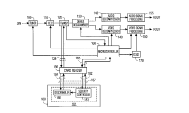
Figure 1 shows, in block diagram form, a signal processing
system including a smart card that provides both entitlement
processing and descrambling;
AMENDED SHEET
WO 96!07267 " ~ ~' ~ ~~~ ~ ~ PCT/US95/09891
Figure 2A shows the location of signal contacts on the
surface of a smart card in accordance with ISO standard 7816-2;
Figure 2B shows the assignment of smart card
interface signals to signal contacts shown in Figure 2A in
5 accordance with ISO standard 7816-2;
Figure 3 shows a format that data included in a signal
processed by the system shown in Figure 1 may exhibit;
Figure 4 shows, in block diagram form, an embodiment
of signal processing functions included in a smart card suitable for
use with the system shown in Figure l;
Figures 5 through 8 illustrate signal routing through
the smart card shown in Figure 4 during various modes of
operation of the system shown in Figure 1;
Figure 9 shows a portion of a signal processing system
including a series-connection of a plurality of smart cards;
Figure 10 shows a television receiver including
features shown in Figure 9; and
Figures 11 and 12 show, in block diagram form,
portions of signal processing systems constructed in accordance
2 0 with principles of the invention.
An embodiment of a smart card access control system
including the invention will be described in reference to an
exemplary video signal processing system that is shown in block
diagram form in Figure 1. The system shown in Figure 1 includes
2 5 signal processing functions that may be found in various signal
processing systems. A specific example is the DSS~ direct-
broadcast satellite television system developed by Thomson
Consumer Electronics, Inc.
For a pay-TV service that involves a smart card based
3 0 access control system, a user wishing to purchase the service
contacts the service provider, pays a service-access fee and
receives a smart card. A card is issued to a user with initial
entitlement information stored in the card's EEPROM. Entitlement
information may include data identifying the user and data
3 5 specifying the scope of initial access entitlement (e.g., duration
SUBSTITUTE SHEET (RULE 26)
,',.,,.
... ...
. ,.: ...
. . . ,.. .. .. ..
6
and/or specific programs the user has paid for). In addition,
application-specific key generation software is stored in the card
memory.
Entitlement information stored in the card can be
modified by the service provider from a remote location using
entitlement management messages (EMM) and entitlement control
messages (ECM) that are inserted into portions of the signal. EMM
includes information indicating subscription (long term access)
and pay-per-view (single program access) services that the user
has paid for. EMM may be directed to a particular smart card by
including identification information in EMM data that corresponds
to the identification information stored in the particular smart
card. ECM includes data such as initialization data needed to
generate descrambling keys. Thus, a signal for a particular
program includes both a scrambled data component comprising
video and audio data, and a control information component
comprising EMM and ECM.
When the user wishes to access a pay-TV service,
2 0 smart card 180 in Figure 1 is inserted into card reader 190. Card
reader 190 couples signals between smart card 180 and a signal
processing channel comprising units 100 through 170 in Figure 1.
More specifically, card reader 190 connects to eight terminals that
are located on the surface of smart card 180 as specified in ISO
2 5 standard 7816-2 (see Figure 2). The connection established by
card reader 190 creates interface 187 between smart card 180
and the signal processing channel. In accordance with an aspect of
the invention described further below, the eight signals in
interface 187 include signals 184 appearing on a high speed data
3 0 input/output (I/O) port for smart card 180, and signals 182
representing a subset of the ISO standard IC card interface signals.
The desired program or service is selected by tuning the
receiver to the appropriate channel using tuner 100. Tuner 100 is
controlled by microcontroller 160 in response to user inputs. For
3 5 example, microcontroller 160 may receive channel selection
signals from a remote control (not shown in Figure 1)
ANIEiVDrJ SHEET
WO 96107267 PCT/L1S95/09891
1964y~~
activated by a user. In response to the channel selection signals,
microcontroller 160 generates control signals causing tuner 100 to
tune the selected channel.
The output of tuner 100 is coupled to forward error
corrector (FEC) 110. FEC 110 monitors error control information,
such as parity bits in the tuned signal, to detect errors and,
depending on the error control protocol, to correct errors.
Microcontroller 160 is coupled to FEC 110 to monitor the
occurrence of errors in the signal and control the processing of
errors. FEC 110 also performs an analog-to-digital conversion
(ADC) function to convert the analog output of tuner 100 to a
digital signal at the output of FEC 110.
Transport unit 120 processes the signal from FEC 110
to detect and separate various types of data in the tuned signal.
The data in the signal may be arranged in various formats. Figure
3 shows an exemplary data format that serves as the basis for the
following description. The signal depicted in Figure 3 comprises a
stream of data organized in packets of data bytes, i.e. "packetized"
data. Each packet is associated with a particular type, or sub-
2 0 stream, of information in the tuned channel's data stream. For
example, the signal includes packets of program-guide
information, control information (e.g., ECM or EMM), video
information, and audio information. The sub-stream that a
particular packet is associated with is defined by data included in
2 5 a header portion of each packet. A payload portion of each packet
includes the packet data. The exemplary data format shown in
Figure 3 includes two bytes ( 16 bits) of data in the header and
186 bytes of data in the payload.
SUBSTITUTE SHEET (RULE 26)
WO 96107267 PCT/US95109891
2196406
s
The first twelve bits of the header in each packet are
program identification (PID) data bits. PID data identifies the data
substream that the payload data is associated with. An example
of the information provided by PID data follows:
TAB 1
PID Value Payload contents
1 program-guide information
4 EMM
10 video data for channel 101
1 1 audio data for channel 101.
Other PID values identify video and audio data for other channels.
As part of the tuning process, microcontroller 160
refers to a PID "map" stored in the microcontroller's memory to
determine the PID values associated with the tuned channel. The
appropriate PID values are loaded into PID registers in transport
unit 120. For example, when channel 101 is selected,
2 0 microcontroller 160 accesses the stored PID map, determines that
video data and audio data for channel 101 are associated with PID
values of 10 and 11, respectively, and loads the values 10 and 11
into respective video and audio PID registers in transport unit
120. The PID data in incoming packets is compared to the PID
2 5 values stored in the PID registers to determine the content of the
payload of each packet. Microcontroller 160 can update the PID
map data in response to PID-to-channel correspondence
information in "program guide" packets (PID value of 1).
SUBSTITUTE SHEET (RULE 26)
WO 96/07267 PCT/US95/09891
~196~06
The last four bits of the header portion of each packet
further define the payload contents as follows:
TABLE 2
S
Header bit Designation Function
1 3 ECM flag indicates if payload is ECM
14 - reserved
15 ENC flag indicates if payload is
encrypted
1 6 Key flag indicates whether payload key
is key A or key B.
1 5 The ECM flag being active, e.g., at logic 1, indicates that the
payload includes ECM data such as initialization data for key
generation. The ENC flag being active indicates that the payload is
encrypted and, therefore, must be descrambled. The key flag
determines which one of two keys, key A or key B, should be used
2 0 for descrambling the payload (e.g., logic 0 indicates key A, logic 1
indicates key B). Use of the key flag is described below in regard
to Figure 7.
Transport unit 120 in Figure 1 extracts and processes
the header data in response to a packet clock signal shown in
:. Figure 3. The packet clock signal is generated and synchronized to
the data stream by FEC 110. Each transition of the packet clock
signal indicates the beginning of a packet. Transport unit 120
processes the 16 , bits of header data following each packet clock
signal transition to determine the destination for the packet
3 0 payload. For example, transport unit 120 transfers payloads
containing EMM (Pm value of 4) and ECM to security controller
183 in smart card 180 via microcontroller 160. Video and audio
data are directed to demux/descrambler 130 for descrambling
and deinultiplexing into video and audio signals. Program guide
SUBSTITUTE SHEET (RULE?~1
w0 96/07267 ' PCT/US95/09891
~ :9x6406
to
data (PID value of 1 ) is directed to microcontroller 160 for PID
map updating.
Security controller 183 processes EMM and ECM data
to provide access control functions including entitlement
management and key generation. Security controller 183 is
included in integrated circuit (IC) 181 and comprises a
microprocessor such as the 6805 processor from Motorola.
Entitlement management involves processing EMM data to
determine how and when entitlement information stored in IC
~ 181 is to be updated, i.e. adding and deleting entitlements. ECM
data provides initial values needed for security controller 183 to
generate descrambling keys. After being generated by security
controller 183, a key is transferred via microcontroller 160 to
descrambler 130 where the scrambled data component of the
input signal, e.g., the video and audio program data, from the
tuned channel is descrambled. In accordance with principles of
the invention that are described further below, the descrambling
function may also be provided by descrambler 185 included in IC
181.
2 0 Descrambled video and audio data is decompressed in
video decompressor 140 and audio decompressor 145,
respectively. Program data is compressed at the program source
using any one of a variety of known data compression algorithms.
Decompressors 140 and 145 reverse the effects of the
2 5 compression algorithm.
The outputs of video and audio decompressors 140
and 145 are coupled to respective video and audio signal
processors 150 and 155. Audio signal processor 155 may include
functions such as stereo signal generation and digital to analog
3 0 conversion for converting the digital output signal from
decompressor 145 to an analog audio output signal AOUT from
processor 155 that can be coupled to a loudspeaker (not shown in
Figure 1 ). Video signal processor 150 also includes digital to
analog conversion capability to convert the digital output of
3 5 decompressor 140 to an analog video output signal VOUT that is
SUBSTITUTE SHEET (RULE 26~
WO 96107267 PCTIUS95/09891
f 9646
11
suitable for display on a display device such as a kinescope.
Video processor 150 also provides signal switching necessary to
include an on-screen display (OSD) signal, produced by OSD
processor 170, in signal VOUT. The OSD signal represents, for
example, graphics information such as a channel number display
that is to be included in the displayed image. Video switches in
video processor 150 multiplex the OSD signal into signal VOUT as
required to produce the desired display. The operation of OSD
processor 170 is controlled by microcontroller 160.
Returning to the access control features of the system
shown in Figure 1, the features and function of smart card 180
may be better understood by referring to the block diagram of
smart card IC 181 that is shown in Figure 4. Reference numerals
in Figure 4 that are the same as in Figure 1 indicate the same or
1 5 similar features. In Figure 4, integrated circuit (IC) 181 includes
security controller 183 comprising a central processing unit (CPU)
421, RAM 426, ROM 425, EEPROM 423 and serial I/O unit 424.
CPU 421 is a processor such as the 6805 from Motorola. Key
generation and entitlement management software is stored in
2 0 ROM 425 and EEPROM 423.
Data specifying current entitlements is also stored in
EEPROM 423 and is modified in response to information in
entitlement management messages (EMM) in the received signal.
When an EMM packet is detected by transport processor 120 in
2 5 Figure 1 (pac'~et rID value of 4), microcontroller 160 in Figure 1
transfers the packet payload to security controller 183 via serial
I/O unit 424. CPU 421 transfers the EMM data in the payload to
RAM 426. ''.PU 421 processes the EMM data and modifies
entitlement da;a stored in EEPROM 423 accordingly.
3 0 . Packet payloads that include entitlement control
messages (ECM), as indicated by the ECM flag in the packet header
being active, are transferred from transport unit 120 to security
controller 183 via microcontroller 160 and serial I/O unit 424.
Any type of packet, e.g., EMM, video, or audio, may include ECM.
3 5 ECM data is used for generating the descrambling key for a
SUBSTITUTE SHEET (RULE 26)
WO 96107267 2 ,~; ~ '; PCT/US95/09891
12
particular type of data. For example, ECM data in an EMM packet
is used to generate an EMM descrambling key. When transferred
to security controller 183, ECM data is stored in RAM 426 until
processed by CPU 421. Key generation software stored in EEPROM
423 and ROM 425 is executed by CPU 421 using the ECM data in
RAM 426 to generate a particular key. The ECM data provides
information such as initial values required by the key generation
algorithms. The resulting key is stored in RAM 426 until
transferred by CPU 421 to descrambler 130 via serial I/O unit
324 and microcontroller 160.
EMM and ECM data may be encrypted as indicated by
encryption flag ENC in the packet header being active. Encrypted
data is transferred from transport unit 120 to descrambler 130
for descrambling before being transferred to security controller
183 for entitlement management or key generation processing.
The features and operation of IC 181 that have been
described are typical of known smart card systems. As stated
above, however, using a descrambling unit external to a smart
card, such as descrambler 130, substantially degrades system
2 0 security and makes changing descrambling hardware undesirable.
The arrangement shown in Figures 1 and 4 includes features that
significantly improve security in comparison to known smart card
systems. In particular, IC 181 of smart card 180 includes
descrambler unit 185 and high data rate synchronous interface
2 5 184 comprising separate serial data in and serial data out lines.
The combination of descrambler 185 and interface 184 makes it
possible for all access control processing to occur within smart
card 180.
In Figure 1, card reader 190 couples both ISO standard
3 0 interface signals 165 from microcontroller 160 and high speed
interface signals 125 from transport unit 120 to smart card 180
via portions of smart card interface 187 that are labeled 182 and
184, respectively. Figure 4 shows the signals included in interface
187. ISO standard signals 182 comprise power, ground, reset, and
3 5 serial I/O in Figure 4 (correspond to VCC, GND, RST, and I/O in
SUBSTITUTE SHEET (RULE 26)
WO 96107267 PCT/US95/09891
?19646
13
Figure 2B). High speed interface signals 184 comprise high speed
data-in and data-out signals, a packet clock signal, and a high
frequency (e.g. 50 MHz) clock signal. ISO standard signal VPP
(programming voltage) is replaced by the packet clock signal
allowing interface 187, including both high and low speed
interfaces, to be implemented using the ISO standard
configuration of eight contacts that is shown in Figure 2A.
Eliminating signal VPP does not preclude the system
shown in Figure 1 from operating with existing ISO standard
smart cards that do not include descrambler 185 and high speed
data interface 184. Existing smart cards typically include EEPROM
circuits that do not require a separate programming voltage. A
"charge pump" feature generates the required programming
voltage from the card supply voltage when programming is
required. Thus, the VPP signal as specified by the ISO standard is
an "unused" terminal for most existing ISO standard smart cards.
Use of the system with existing smart cards does require
modifying the operation of the system such that high speed
interface 184 and descrambler 185 are not used. The required
2 0 modification can be achieved by changing only the control
software for controller 160.
Descrambler 185 operates at a high data rate in
response to the high frequency clock signal while security
controller 183 requires a lower frequency clock signal. Divider
2 5 422 in IC 181 divides the SC MHz clock signal to produce a lower
frequency clock signal suitable for security controller 183. Thus,
the single high frequenr~y clock signal serves as a timing signal for
controlling the operation of both security controller 183 and
descrambler 185.' Using divider 422 avoids dedicating two of the
3 0 eight smart card interface signals to separate high and low
frequency clock signals.
Descrambler 185 includes transport decode unit 472,
PID & ECM filter unit 474 and EMM address filter unit 476 for
providing functions similar to the above-described functions of
3 5 transport unit 120 in Figure 1. The high speed data-in and data-
SUBSTITUTE SI~~ET (RULE 26)
WO 96/07267 PCTIUS95/09891
14 X196406
out signals of interface 187 couple the high speed data stream of
the input signal between transport unit 120 and descrambler 185.
Including functions of transport unit 120 within smart card 180
enables smart card 180 to process incoming data packets at the
high data rate of the input signal. Both the data-in and packet
clock signals are coupled to unit 472.
In response to each transition in the packet clock
signal, unit 472 processes the 16 bits of header data. The first 12
bits of the header are program identification (PID) data that are
1 0 directed to PID & ECM filter unit 474. Unit 474 compares the
packet's PID data to PID values stored in unit 474 for each type of
packet included in the tuned chan: gel. Similarly to the above-
described operation of transport unit 120 (see Table 1 above and
associated description), PID comparison in unit 474 determines
what type of data the payload contains, e.g., program guide, EMM,
video, or audio. PID values identifying packet types in the
currently tuned signal are stored in registers in unit 474. The
registers are loaded as part of the above-described tuning process
for the system in Figure 1. More specifically, microcontroller 160
2 0 accesses a stored PID "map" as described above and transfers PID
values associated with the currently tuned channel to registers in
unit 474 via signals 182 and security controller 183 in smart card
180. Transfer of data betwreen security controller 183 and
functions of descrambler 185, such as unit 474, occurs via a data
2 5 bus internal to IC 181 that is not shown in Figure 4.
How the payload data is processed by smart card 180
is determined both by the results of PID comparison in unit 474
and by the contents of bits 13 to 16 of the packet header
extracted by unit 472. Using the ~ example above relating to
3 0 channel 101 (see Table 1), PID data identifies: program guide data
(PID = 1 ) that microcontroller 160 processes to update the PID
map, EMM data (PID = 4) that security controller 183 processes to
modify entitlements, video data (PID = 10) and audio data (PID =
11 ). Bits 13 through 16 of the header control security-related
3 5 operations (see Table 2 above and the associated description) in
SUBSTITUTE SHEET (RULE 26)
WO 96/07267 PCT/L1S95/09891
smart card 180. If bit 13 (ECM flag) is active, the payload
includes ECM data that requires key generation processing by
security controller 183. If bit 15 (ENC flag) is active, the payload
is encrypted and is descrambled in descrambling unit 478 within
5 descrambler 185. Bit 16 determines whether key A or key B will
be used in unit 478 for descrambling.
The encryption status bit ENC determines how payload
data will be processed by descrambling unit 478. Payload data
that is not encrypted passes unchanged from the high speed data-
10 in terminal of smart card 180 through descrambling unit 478 to
the high speed data-out terminal. Encrypted data is descrambled
at the data rate by unit 478. Descrambled video and audio data is
passed to the high speed data-out terminal of smart card 180. In
each descrambled audio or video packet, the ENC bit in the packet
1 5 header is set to logic 0 indicating that the packet is "clear", i.e.
descrambled. To ensure that unauthorized users do not access
entitlement or key related data, descrambled EMM or ECM data is
not passed out of smart card 180 via the high speed data our
terminal. Instead, the original scrambled EMM or ECM data, with
2 0 the ENC bit set to logic 1, is passed through smart card 180 from
the high speed data-in terminal to the high speed data-out
terminal. EMM and ECM data that is descrambled in descrambling
unit 478 is stored temporarily in RAM 426 in security controller
183 until processed by security controller 183 for entitlement
2 5 management and key generation. Transport snit 120 in Figure 1
receives the data (either unchanged or descrambled) from the
high speed data-out terminal of smart card 180. The PID value of
each packet is checked and the payload is r~ansferred to the
appropriate function in Figure 1 for further processing (e.g.,
3 0 microcontroller 160 or decompressors 140 and 145).
The operation of smart card 18C is controlled by
commands from microcontroller 160 in Figure 1 that are
communicated to smart card 180 via the ISO standard serial
interface. In effect, microcontroller 160 is the master processor
3 5 and security controller 183 is the slave processor. For example,
SUBSTITUTE SHEET (RULE 26)
WO 96107267 PCT/US95/09891
16 ~ 196406
microcontroller 160 transfers PID information to smart card 180
and directs the card to descramble the data in the corresponding
data streams. Security controller 183 responds by checking
entitlements and configuring smart card 180 for the appropriate
type of data processing such as entitlement processing, key
generation or descrambling. In addition, microcontroller 160
requests status information such as whether descrambling is in
progress. Commands are communicated to security controller 183
in smart card 180 via the serial I/O terminal. Any response
required by the command is returned to microcontroller 160 via
the serial I/O terminal. Thus, the serial I/O signal serves as a
control signal between the system and smart card 180 while the
high-speed data interface provides high-speed input and output
data signals between the card and the system.
Serial communications between microcontroller 160
and smart card 180 occur according to a protocol provided for in
ISO standard 7816-3. A smart card notifies -the system of the
particular protocol that will be used by sending a protocol type
number T to the system. More specifically, when a card is
2 0 inserted into the card reader, the card reader applies power to the
card and resets the card by activating the reset signal. The card
responds to the reset signal with an "answer to reset" data
sequence specified in ISO standard 7816-3 ~6. The answer to
reset includes an interface byte TDi. The four least significant of
2 S byte TDi define the protocol type number T (see ISO standard
7816-3 ~6.1.4.3).
The protocol type for the system shown in Figure 1 is
type T=5. A type 5 protocol is classified as "reserved", i.e.
currently undefined, in the ISO standard. For the system in Figure
3 0 1, protocol type 5 is identical to protocol type 0 (an asynchronous
half-duplex protocol defined in ISO 7816-3 ~8) except for the
manner in which the baud rate for serial I/O is determined. Serial
I/O at the card interface occurs at a rate determined according to
Table 6 in ISO standard 7816-3. The baud rate calculation is
3 5 based on the rate at which security controller 183 is clocked. For
SUBSTITUTE SHEET (RULE'6)
WO 96!07267 PCT/US95109891
17 2196406
existing smart cards, the clock frequency for security controller
183 is equal to the clock frequency fs at the card's clock pin. As
shown in Figure 4, smart card 180 includes divider 422 for
dividing the rate of the high speed input clock Fin by a factor N,
i.e. Fin/N, to establish the clock rate for security controller 183.
Thus, for a type 5 protocol, Table 6 of ISO standard 7816-3 is
modified by defining fs = Fin/N.
As in the case of a type 0 protocol, all commands for a
type 5 protocol are initiated by microcontroller 160. A command
begins with a five byte header including a one-byte instruction
class designation (CLA), a one-byte instruction (INS), a two-byte
parameter (P1,P2) such as an address, and a one-byte number
(P3) defining the number of data bytes that are part of the
command and follow the header. For the system in Figure l,
parameter P1,P2 is not needed and, therefore, these bytes are
"don't cares". Thus, commands take the form:
CLA I INS I - I - I P3 I data (P3 bytes).
2 0 . Commands recognized by smart card 160 include a
status command and a PID transfer command. Smart card 160
responds to a status command from microcontroller 160 by
providing the processing status of the card, e.g. whether the card
has completed key generation or whether the card is
2 S descrambling data. Using a PID transfer command,
microcontroller 160 transfers PID numbers associated with the
tuned channel. Other commands such as commands fo:-
transferring EMM and ECM data, key related commands, and
"purchase offer" commands are possible and will be exploined
3 0 below.
The operation of smart card 180, and in particular
descrambler 185, will now be described in more detail in
reference to Figures 5 through 8. When a new channel is tuned,
microcontroller 160 transfers PID values for the new channel
3 5 from the PID map to smart card 180 as shown in Figure 5. The
SUBSTITUTE SHEET RULE 26)
WO 96!07267 PCT/US95I09891
X196406
is
PID data transfer occurs using a PID transfer command including
N PID values, where N is specified in byte P3 of the command
header. The command and PID values are communicated to the
card via the serial data terminal of smart card 180 and serial
input/output unit 424. CPU 421 receives the PID data and directs
the data to the appropriate PID register in registers 474 in
descrambler 185.
Before a signal can be descrambled, a user must be
entitled to access and the correct key must be loaded into
descrambler 185. After transfer of the PID data to smart card
180, security controller 183 compares the PID values to
entitlement data stored in EEPROM 423 to see if the user is
entitled to access the tuned channel. Assuming the user is
entitled, the next step is key generation. Key generation involves
1 5 processing ECM data. Thus, ECM must be received and processed
to produce the key before audio and video data can be
descrambled. ECM data is encrypted to reduce the likelihood of
unauthorized key generation. A card is issued with a key for
descrambling ECM stored in the card in EEPROM 423. As
2 0 illustrated in Figure 6, the ECM key is transferred by CPU 421
from EEPROM 423 to ECM key registers in descrambling unit 478.
If the user is not entitled to access the tuned channel,
entitlements must be received before key generation and
descrambling can occur. Entitlements can be received via EMM.
2 5 An "address" identifying a particular smart card is stored in EMM
address unit 476 of the card when the card is issued. By including
address information in EMM, a service provider can direct EMM to
a particular card. The smart card compares the address
information in EMM with the card address stored in unit 476 to
3 0 detect EMM information directed to the card. If a user is not
entitled, security controller 183 configures the card for EMM
processing as shown in Figure 6 in case EMM data is received.
As in the case of the ECM key, a card is issued with an
EMM key stored in the card in EEPROM 423. In Figure 6, the EMM
3 5 key is transferred from EEPROM 423 to EMM key registers in
SUBSTITUTE SHEET (RU~.E 26)
WO 96!07267 PCT/US95109891
~:,~ 9 ~4~b
19
descrambling unit 478 by CPU 421. Scrambled EMM data from
transport unit 120 in Figure 1 is input to the card via the high
speed data-in port. After checking the EMM address in unit 476,
EMM data intended for the card is decrypted in descrambling unit
478. Decrypted EMM data is temporarily stored in RAM 426 and
processed by CPU 421 to update entitlement data stored in
EEPROM 423.
After . the PID values are loaded, entitlements exist,
and the ECM key is in place in descrambler 185, the card is ready
to descramble ECM data and generate the audio and video keys.
In Figure 7, ECM data in the signal is received by smart card 180
via the high speed data-in terminal and detected by transport
decode unit 472. The ECM data is directed to descrambler 478
where the previously loaded ECM key is used to decrypt the ECM
data. The decrypted ECM data is transferred from descrambler
478 to RAM 424. When decrypted ECM data is available, CPU 421
executes key generation algorithms stored in EEPROM 423 and
ROM 425 using the decrypted ECM data in RAM 424 to generate
the video and audio keys. The generated keys are transferred to
2 0 the appropriate video and audio key registers in descrambler 478.
As shown in Figure 7, descrambler 478 includes two
key registers for video, video keys A and B, and two key registers
for audio, audio keys A and B. Whether key A or B will be used to
descramble a particular packet is determined by the key flag bit
2 5 in the packet header (see Table 2 above). The "multi-key" feature
is used to permit a new key to be generated while an existing key
is being used to descramble data. Processing ECM data in security
controller 183 to generate a new key and transferring the new
key to a key register in descrambler 478 requires a significant
3 0 number of instruction cycles in CPU 421. If descrambling was
halted during the generation and transfer of a new key, the
processing delay would require someone viewing a program to
watch a scrambled image until the new key was in place in
descrainbler 478. Having key registers A and B permits data to
3 5 be decrypted using a key in one key register, e.g., key register A,
SUBSTITUTE SHEET (RULE 2G)
WO 96/07267 - PCT/US95/09891
while a new key is being generated and loaded into the second
key register, e.g., key register B. After initiating key generation
by transmitting ECM data, a service provider waits for a time
period sufficient to ensure that new key B is generated and in
5 descrambler 478 before encrypting packets using key B. The key
flag notifies descrambler 185 when to begin using the new key.
After the operations shown in Figures 5, 6, and 7,
descrambler 478 has been initialized with all key information
needed to process encrypted data in the tuned channel, including
1 0 EMM, ECM, video and audio data. Figure 8 shows the signal flow
for data processing. Encrypted data enters smart card 180 via the
high speed serial data input terminal. The data is decrypted in
descrambler 478 using the previously loaded keys. For example,
if transport unit 472 determines from the header of an incoming
15 packet that the payload data is video data associated with video
key A, the packet payload is decrypted in descrambler 478 using
video key A. The decrypted data is output directly from smart
card 180 via the high speed serial data output terminal. Note that
data processing in Figure 8 does not require interaction between
2 0 descrambling unit 185 and security control unit 183 allowing
descrambler 478 to process data at the high data rate of the input
signal.
Key generation in security controller 183 combined
with the descrambling features of descrambling unit 478 provides
2 5 complete capability in smart card 180 for processing signals
encrypted using a variety of algorithms including the data
encryption standard (DES) algorithm and Rivest-Shamir-
Adlemann (RSA) algorithms. By providing all access control
related processing within smart card 180, security related data
3 0 such as key data does not have to be transferred out of smart card
180. As a result, security is improved significantly in comparison
to systems using a descrambler external to the smart card.
Although the use of descrambler 185 internal to smart
card 1'80 is advantageous, an external descrambler such as
3 5 descrambler 130 in Figure 1 may also be used. An external
SUBSTITUTE SHEET (RULE 26)
WO 96!07267 PCTIUS95/09891
21 2196406
descrambler may be desirable for compatibility of the described
smart card with existing pay-TV systems that generate the key in
smart card 180 and transfer the key to descrambler 130.
Alternatively, using both descrambler 185 and descrambler 130
may be desirable. For example, security can be improved by
encrypting a signal twice using two different keys. A twice-
encrypted signal could be decrypted using the system shown in
Figure 1 by: decrypting the signal once in descrambler 185 using
the first key, transferring the partially decoded data to
descrambler 130, and decrypting the signal a second time in
descrambler 130 using the second key. The second key would be
generated in smart card 180 and transferred to descrambler 130.
For applications involving descrambler 130 (i.e.
applications in which key data is transferred out of smart card
180), commands are provided for transferring the key data via
the serial UO interface between controller 160 and smart card
180. For example, microcontroller 160 sends ECM data to the card
in one command and requests the status of key generation with a
status command. When the status data indicates that key
2 0 generation is complete, another command requests the key data
and the card responds by sending the key data to controller 160.
Subsequently, the key is transferred to descrambler 130.
Modifying the system in Figure 1 in accordance with
principles of the invention permits processing data via an
2 5 arrangement of a plurality of smart cards in which the high speed
data paths of the cards are connected in series. More specifically,
the high speed data-out terminal of one card is connected to the
high speed data-in terminal of the next card. As will be described
in regard to Figures 9 through 12, a system processing video data
3 0 via series connected smart cards can use multiple access-
controlled signals, such as pay-TV signals, to provide features
such as picture-in-picture (pix-in-pix or PIP) and picture-outside-
picture (POP) in a video system such as a television receiver. For
example, a PIP feature generates a signal representing both a
3 5 main video picture and one or more small pictures that are inset
SUBSTITUTE SHEET (RULE 26)
WO 96/07267 ' PCT/US95/09891
L 196406
22
into a portion of the main picture. In a television receiver, the
main picture may be produced in response to the signal from one
television channel while the inset picture is produced in response
to the signal from a second television channel. Using a series
connection of two or more smart cards, one smart card processes a
first signal, e.g., descrambles a pay-TV signal, to provide the main
picture while one or more additional smart cards process one or
more other signals, such as other pay-TV signals, to provide the
inset picture or pictures.
~ Figure 9 shows a switching arrangement for use in a
smart card reader to provide the described series-connected high
speed data path. In Figure 9, switches 1 and 2 are responsive to
the insertion of cards 1 and 2, respectively, into the card reader.
Switches 1 and 2 determine the routing of the high speed DATAIN
and DATAOUT signals to the descrambler in the respective smart
card. Each switch is shown as a single-pole-single-throw (SPST)
switch that will be in one of two possible states, A or B, depending
on whether or not the corresponding card is inserted: state A if
the respective card is not inserted, and state B if the card is
2 0 inserted. In state A, a switch causes input data, i.e. signal
DATAIN, to bypass the corresponding card. In state B, input data
is connected to the inserted card.
In Figure 9, both cards 1 and 2 are inserted causing
both switches 1 and 2 to be in position B. As a result, high speed
2 5 data is routed from DATAIN through cards 1 and 2 in series. If
only a single card is being used, card 2 is not inserted, switch S2 is
in position A, and high speed data bypasses card 2. The switching
configurations for the arrangement in Figure 9 are listed in Table
3.
SUBSTfTUTE SHEET (RUtf 26)
WO 96/07267 PCT/US95/09891
~~96406
23
TABLE 3
Card Status SwitchPosition
r 1 Car 2 ~1 ~2 Connection
inserted inserted B B DATAIN to DIN1;
DOUT 1 to DIN2;
DOUT2 to DATAOUT
inserted removed B A DATAIN to DIN1;
DOUT 1 to DATAOUT
(bypass card 2)
removed removed A A DATAIN to DATAOUT
(bypass cards 1 & 2)
The operation of the high speed data signal switching
1 5 arrangement shown in Figure 9 involves signals S 1 CTRL, S2 CTRL,
CARD1 INSERTED and CARD2 INSERTED. Switches S1 and S2 are
electronic switches controlled by signals S 1 CTRL and S2 CTRL,
respectively. The switch control signals are generated by a
control processor either in the card reader or in the system (e.g.,
2 0 microcontroller 160 in Figure 1 ) in response to signals CARD 1
INSERTED and CARD2 INSERTED. Signals CARD1 INSERTED and
CARD2 INSERTED are generated by switches S3 and S4,
respectively, in response to the insertion of the corresponding
card and are coupled to respective interrupt inputs of
2 ~ m::;rocontroller 160.
Before card 1 is inserted, signal S 1 CTRL is at logic 0
causing electronic switch S 1 to be at position A and signal DATAIN
bypasses card 1. , Inserting card 1 into the card reader causes
switch S3 to change from position ~A (card removed) to position B
3 l; (card inserted). As a result, signal CARD 1 INSERTED changes from
logic 1 (+ supply voltage) to logic 0 (ground). The interrupt
handling routine of microcontroller 160 detects the change in
signal CARD 1 INSERTED and changes the level of signal S 1 CTRL.
Switch S 1 responds by changing to position B coupling signal
SUBSTITUTE SHEET (RULE 26)
WO 96!07267 ~ ,~ 9 6 4 0 6 PCT/US95/09891
24
DATAIN to card 1. Switches S2 and S4 operate in a similar
manner in response to card 2 being inserted.
The described card reader operation routes the high
speed data signal through the descrambler of each card inserted
in the card reader. For descrambling a signal that was encrypted
more than once, each descrambler in the series connection
descrambles the signal using a particular key and algorithm. For a
series connection .of cards in which each card corresponds to a
particular service, each card descrambles data for the service
associated with the card and passes other data unchanged.
Selective descrambling in each card is accomplished by PID
processing in each card. The PID registers in each card are loaded
with the PID values for the service corresponding to the card.
Each card checks the PID data in the header of each packet in the
1 5 signal. If the PID data does not correspond to the PID data stored
in the card, the data passes through the card unchanged. A packet
payload is descrambled only in a card in which the card PID data
matches the packet PID data.
Control of a mufti-card series-connected "stack" such
2 0 as that shown in Figure 9 is accomplished via the ISO standard
serial I/O signal. In addition to the high-speed data I/O signals
shown in Figure 9, smart card interface signals "clock", "packet
clock", "power" and "ground" (see Figure 4 and associated
description) are coupled to each card inserted in card reader 190.
2 5 Interface signals "serial I/O" and "reset" are coupled to only one
smart card at any particular time. Controller 160 detects that a
card is inserted via signals CARD 1 INSERTED or C.ARD2 INSERTED
and controls switch SS to couple the serial UO and reset signals to
an inserted card, ' as needed, to transfer data to the card. If more
3 0 than one card is inserted, controller 160 communicates with a
particular card by controlling switch SS to couple the serial I/O
and reset signals to only that particular card. The flow of high
speed data through each card in the serially-connected stack of
cards is not affected by the operation of switch S5.
SUBSTITUTE SHEET (RULE 26)
WO 96107267
i PCT/US95109891
~54~b
One aspect of the control of a card stack involves a
delay between high speed data and the packet clock signal that
depends on the location in the stack of a particular card. The high
speed data path of a smart card exhibits a bit delay from data-in
5 to data-out equal to the number of high speed clock cycles
required for the data processing operation that is occurring in the
card. A card that is merely passing data from data-in to data-out
will create a different bit delay than a card that is descrambling
data. The series connection of cards in the stack causes high
1 0 speed data arriving at a particular card in the stack to exhibit a
bit delay with respect to packet clock that depends on the number
of cards in the stack prior to a particular card and the type of
processing occurring in each card prior to a particular card.
If the bit delay is not corrected, cards in the stack
15 other than the first card will process the packetized data stream
improperly. For example, packet header data is extracted based
on the occurrence of transitions in the packet clock signal. A bit
delay with respect to packet clock will result in improper
extraction of the header data and, subsequently, incorrect
2 0 processing of the payload data.
Correcting for bit delays is accomplished by
communicating bit delay information between controller 160 and
security controller 183 of each card in the stack. Each card
returns its particular bit delay value to controller 160 in response
2 5 to a com~aand from controller 160. A card determines its current
bit delay by, for example, referring to a look-up table in the card
memos r that specifies a bit delay value for each data processing
mode, i. ~. descrambling, pass-through, etc. Controller 160
acquires tire bit delay data for each card in the stack and sends to
3 0 each carol information including: the number of cards in the stack,
the position of the card in the stack (e.g., card 2) and the bit delay
for all cards in the stack prior to the particular card. The card
corrects for bit delay by, for example, using the stack bit delay
information from controller 160 to control a variable delay circuit
3 5 included in the packet clock signal path within transport unit 478.
SUBSTITUTE SHEET (RULE 26)
WO 96/07267 PCT/US95/09891
?? ~b406
26
The arrangement shown in Figure 9 for reading a
plurality of smart cards can be included in a television receiver.
For example, Figure 10 shows a television receiver 1000 including
the capability for simultaneously reading two smart cards. Two
cards are inserted in slots 1010 and 1020. Card reading circuitry
similar to circuitry shown in Figure 9 is included in receiver 1000
to produce the above-described series connection of two smart
cards. As will be described further in regard to Figures 11 and
12, first and second smart cards inserted in slots 1010 and 1020
in Figure 10 process respective pay-TV signals to provide a PIP
feature that produces main picture 1030 and inset picture 1040.
Figure 11 shows a portion of a system for processing a
video signal through smart cards 180 and 1805 connected in
series in the manner described in regard to Figure 9. Each smart
card includes features described in regard to Figures 1 and 4-8.
Reference numerals used in Figure 11 that also appear in Figure 1
identify the same or similar features. Features common to Figures
1 and 11 are explained above in detail in the description of Figure
1. Figures 11 and 12 will be described in the context of
2 0 processing television signals, but other video signals may be
processed in a similar manner.
As described above in regard to Figure 1, tuner 100,
forward error corrector (FEC) 110 and transport unit (TRANSP)
120 in Figure 11 process input signal SIN under control of
2 5 controller (u C) 160 to produce an output signal TRO from
transport unit 120 that includes data representing desired
television programs. To provide a multi-image display feature
such as PIP or POP in which the main and small pictures
correspond to different television programs, signal TRO from
3 0 transport unit 120 includes a signal component corresponding to
each program. Using the above-described packetized signal
format as an example, a first component of signal TRO includes a
first group of data packets exhibiting a first PID value
corresponding to the first television program. A second
3 5 component of signal TRO includes a second group of packets
SUBSTITUTE SHEET (RULE 26)
WO 96107267
19 6 4 0 6 PCT~S95/09891
27
exhibiting a second PID value corresponding to the second
television program. Each of the two components of signal TRO
may be scrambled.
Signal TRO is coupled to high speed data input DI1 of
first smart 180 via card reader 190. Smart card 180 processes a
first one of the two components of signal TRO, e.g., the component
representing the program that will appear in the main picture.
Processing in smart card 180 includes descrambling of the data in
the component if the data is scrambled. High speed data output
signal DO1 from the first smart card includes the processed first
component, e.g., descrambled, and the unprocessed second
component. As explained above in regard to Figure 9, card reader
190 connects the high speed data path of smart card 180 in series
with the high speed data path of second smart card 1805 by
1 5 coupling data output DO1 of first smart card 180 to data input DI2
of second smart card 1805. Smart card 1805 processes the second
component of the signal, including descrambling as required, to
produce high speed data output signal D02. Signal D02 includes
the processed first component and the processed second
2 0 component. If both components of signal TRO ~ were scrambled,
signal D02 includes first and second descrambled components
corresponding to the original scrambled components.
Signal D02 is returned to transport unit 120 via card
reader 190 for routing to other functions in the system. As an
2 5 example, to produce a PIP display, signal D02 is routed to de-
multiplexer (DEMUX) 130 that separates the first and second
processed signal components under control of controller 160. The
first and second processed ;signal components are decompressed in
decompressor units 140 and :405, respectively. The
3 0 decompressed data undergoes further processing in signal
processors 150 and 1505. In the case of creating a small picture
such as for a PIP or POP display, the one of processors 150 and
1505 that processes the small picture signal may include video
memory for storing and accessing data corresponding to the small
3 5 picture. The signals output by processors 150 and 1505 are
SUBSTITUTE SHEET (RULE 26)
WO 96107267 PCT/US95109891
~' 9640b
28
combined by multiplexes (MUX), or switch, 1506, to provide a
signal that will produce the desired image including a small
picture in the desired portion of the image. Controller 160
controls the timing of MUX 1506 to insert the signal component
corresponding to the small picture at the appropriate time.
Output processor 1507 couples the image signal to a display
device such as kinescope 1508. Functions such as contrast control
brightness control and kinescope driver amplification are
provided by output processor 1507.
The system shown in Figure 11 provides the desired
mufti-image feature when signal DI1 at the data input of first
smart card 180 includes first and second signal components
representing first and second television programs as described.
Such is the case if the signal tuned by tuner 100 includes both
1 5 components or, for example, if signal DI1 is provided by a source
other than the tuner, FEC and transport units shown in Figure 11
that provides a signal including both components. An example of
an alternative signal source is a cable television signal that
includes signal components corresponding to various channels.
2 0 ~ In the case of a signal received directly from a satellite
such as the DSS~ signal described above, signal SIN in Figure 11
includes signals at various frequencies produced by the various
transponders of the satellite. Tuner 100 tunes only one of the
transponder signals at a time. Although each tuned transponder
2 5 signal includes signal components corresponding to a plurality of
television programs, the signal components needed to produce a
mufti-image display, e.g., the main and small picture channels
selected by a user, may be received via different transponders.
If so, the signal tuned by tuner 100 (and signals TRO and DI1 )
3 0 includes only one of the signal components required to produce
the desired mufti-image display. This situation is addressed by
the system shown in Figure 12.
In Figure 12, tuner 101, FEC 111, transport unit 121,
and multiplexes (MUX) 127 are added to the system shown in
3 5 Figure 11. Tuner 100, FEC 110 and transport unit 120 tune the
SUBSTITUTE SHEET (RULE 26~
WO 96107267 PCT/LTS95/09891
29 ~ 196406
signal from one transponder and produce signal TRO1 that
includes one of the signal components needed to produce the
multi-image display. Tuner 101, FEC 111 and transport unit 121
tune the signal from a second transponder and produce signal
TR02 that includes a second one of the required signal
components. MUX 127 combines signals TRO1 and TR02 under
control of controller 160 to produce a signal at the output of MUX
127 that includes both of the required signal components. The
MUX output signal is coupled to the first smart card via card
reader 190 and processed as described above in regard to Figure
11 to produce the desired mufti-image display.
Various modifications of the described embodiments
are possible. It will be readily apparent to one skilled in the art
that the invention is applicable to video systems and video signal
1 5 protocols other than that depicted in Figures 3, 11 and 12.
Examples of other systems are the above-mentioned DSS~ satellite
system and high-definition television (HDTV). Also, the
arrangements shown in Figures 9 through 12 may be expanded to
accommodate . more than two smart cards. For example, in Figure
2 0 9, a switch and card detection capability (i.e. generating a CARD
INSERTED signal) is added for each additional card. Adding smart
cards would permit descrambling more than two signal
components and producing displays including an image portion
corresponding to each descrambled signal component. In addition,
2 5 the switching arrangement in Figure 9 c.;uld be modified to
control switches S 1 and S2 directly in response to cards being
inserted rather than relying on control by microcontroller 160.
For example, switch S3 could be mechanically, or electrically,
coupled directly .to switch S 1 such that inserting card 1 causes
3 0 switch S 1 to route data through card 1. Also, although the
described embodiments relate to digital I/O signals coupled to
smart card 180, smart card 180 may also process analog signals.
For example, smart card 180 may include an analog to digital
converter (ADC) at the high-speed data input and a digital-to-
3 5 analog converter (DAC) at the high-speed data output. The ADC
SUBSTlTlJTE SHEET (RULE 26)
WO 96/07267 - PCT/US95/09891
2196406
and DAC may be located on IC 181 in Figure 1. Alternatively, IC
181 may be replaced with a "hybrid" device, i.e. rather than just
IC 181, smart card 180 would include ADC and DAC circuits and IC
181 all mounted and interconnected on a single substrate. For an
5 analog signal processing smart card, card reader 190 would couple
analog signals to the smart card. These and other modifications
are intended to be within the scope of the following claims:
SUBSTITUTE SHEET (RULE 26)