Note: Descriptions are shown in the official language in which they were submitted.
` _ ( 2196951
Speci~lcation
3"ELECTRONIC SIGNAL MEASUREMENT APPARATUS
4FOR THE ACQUISITION AND DISPLAY
5OF SHORT-DURATION ANALOG SIGNAL EVENTS"
7 BACKGROUND OF THE INVENTION
8 Field of the Invention
9 The present invention relates generally to electronic signal mea~u~ ;lll apl?alalus,
and more particularly to a short-duration analog signal events acquisition and display system
11 wherein the m"ximllm and ~ .;---, m,~gnitudes of a varying analog signal are detected by
12 peak and valley detectors and then ligiti7P~l by an analog-to-digital convellel, stored and
13 then read out at a slower rate for display in electronic strip chart format to highlight signal
14 anomalies.
16 Desc~;l,lion of the Prior Art
17 In the automotive repair field, as well as in other fields, it has long been illli)Oltàlll
18 to have instruments available for obsel~ g electrical signals occurring at various points
19 within the numerous electrical circuits and signal paths resident in an automobile.
Measurements of parameters such as current, voltage, resi~t~n~e, signal frequency, etc.
21 enable a repair technician to locate and diagnose the numerous problems that occur in a
22 vehicle. Such parameters are typically measured using available appdldlus ranging from
23 simple voltage, current and re-ci~t~n~-e-measuring meters to sophictic~t~l, colllLJul~d
24 electronic diagnostic equipment.
Among the most difficult conditions to measure are the interrnittent faults commonly
26 referred to as "glitches", i.e., rapid signal transitions of short duration. Previous
27 measurement systems have either sampled the input analog signals slowly and have thereby
28 ignored rapidly varying signal components, or have sought to detect the rapidly varying
29 components by sampling at a rate higher than the rate of change of the signal. Sampling
39822 U.S. Palenl Ap~ ion -- Pa~e 1 54213 0047
21969Sl
~ (
systems which sample at frequencies higher than the input signal frequency are well known
2 in the art. For example, an oscilloscope which operates under this general plhlcipal
3 contains complex and expensive electronics. At lower sampling rates, glitches might not
4 be captured by the oscilloscope; at higher sampling rates, glitches are less likely to be
S displayed. Furthermore, the extra data derived from the much higher sampling rate, when
6 converted to digital form, requires substantial computational capacity. A major shortcoming
7 of the digital oscilloscope is the loss of data that usually occurs following the analog-to-
8 digital conversion. Glitches occurring on the signal are generally captured by the
9 conversion, but not all captured data is displayed.
Another difficulty with prior art sampling systems is that they use complicated
11 electronics for triggering the capture of short-duration analog signal events. Prior art
12 devices have typically utilized both trigger-level and trigger-delay circuitry. Trigger-level
13 cil.;uill~ will allow detection of an event if its voltage potential rises above a certain preset
14 level. Trigger-delay cil.;uiL.y will delay detection of an event for a preset time period after
the trigger-level circuitry has noted an event with a voltage potential above its preset level.
16 While both of these techniques allow very accurate detection in voltage potential and time
17 of oc-;ullellce, the info"llation obtained is superfluous if all one really needs to know is that
18 a particular event has occurred during a particular time period.
19 A further diff1culty with prior art sampling systems is that if the prior art sampling
system uses a single A/D COII~ r on a multiple input-channel device, the sample rate is
21 reduced by l/n for n ch~nn~l~, further reducing the likelihood of ~et~ctin~ a glitch.
22 There is thus a need for a relatively simple means for ~let~cting and indicating the
23 occurrence of glitches in electrical circuits. Furthermore, there is a need for a device that
24 "latches" a glitch and displays its occ~lllellce in one of several selectable histogrammic
formats so that the user does not have to carefully watch the indicator to notice the transient
26 occurrence of a glitch.
39822 U.S. Pa~ent Applicalion -- Page 2 54213 0047
219~951
SUMMARY OF THE INVENTION
2 It is therefore an object of the present invention to provide an h~ oved appa~us
3 for monilc,lillg electrical signals to detect and indicate the oc~;ullence of rapidly varying
4 analog events, commonly referred to as glitches.
Another objective of the present invention is to provide glitch-detection and display
6 apparatus that is simple to use and relatively low in cost.
7 Another object of the present invention is to provide apparatus of the type described
8 which allows WOIktl:j not experienced in the use of complex test i~ulllents to observe
9 short duration faults.
Still another object of the present invention is to provide app~ us of the type
11 described that does not rely upon the use of fast sample rates to detect and display faults,
12 and does not rely on user observation of the fault at the instant of its oc ;ulle~ce.
13 Yet another object of the present invention is to provide a system of the type
14 described for delecLi"g rapidly varying analog events using limited co~ uL~lional ca~acily
by sampling at a relatively slow rate compared with the analog event to be ~let~ted
16 Briefly, the present invention is embodied in the form of a hand-held instrument
17 which inrh1des m~ximllm and ",i~i",u"~ signal value detection circuits for c~pt~,.;"g the
18 extremes of a rapidly cl~"gi,~ analog signal. The captured values are then fiigi~i7~ by a
19 an analog-to-digital collvellel to generate data which can be stored and subsequently read
out from memory and displayed in the form of a histogram evidencing the ocl;ul~ ce or
21 lack of oc~;ull~llce of a particular type of signal event.
æ An important advantage of the present invention is that it in(~ tes the oc.;ull~ ce
23 of otherwise difficult-to-detect events in a readily perceptible fashion.
24 Another advantage of the present invention is that it provides a histographic display
of the occurrence of the events over a period of time.
26 Still another advantage of the present invention is that it can be used by workers
27 inexperienced in the use of sophisticated test equipment.
28 These and other objects and advantages of the present invention will no doubt
29 become apparent to those skilled in the art after having read the following detailed
39822 U.S. Patent Applic~tion -- P~g~ 3 54213 0047
2196951
description of the preferred embodiment which is illustrated in the several figures of the
2 drawing.
4 IN THE DRAVV~G
Fig. 1 is a diagram illustrating a typical voltage wave form including glitches of the
6 type encountered in automotive diagnostics;
7 Fig. 2 is a diagram illustrating a typical oscilloscope type display of a portion of the
8 wave form illustrated in Fig. 1;
9 Fig. 3 is a display in realtime or near realtime of the wave form illustrated in Fig.
1 during a particular sample period;
11 Fig. 4 is a diagram generally illllstr~ting the operative concept of the present
12 invention;
13 Fig. 5 is a block diagram illustrating the plh~i~al functional components of a signal
14 measurement and display apparatus in accordance with the present invention;
Fig. 6 is an illustration of one type of graphical display provided by appal~lus in
16 accordance with the present invention; and
17 Fig. 7 is a sr~ tir circuit diagram illustrating peak and valley detection circuits
18 in accordance with the present invention.
19
DETAILED DESCRIPTION OF THE PREFERRED EMBODIMENT
21 Referring now to Fig. 1 of the drawing, which depicts at 10 an ~ l;.. g signal
22 trace typical of the type of signal that might be detecte-3 in an automotive circuit. Depicted
23 at 12 and 14 are signal glitches of the type mentioned above, i.e., random voltage spikes
24 of very short duration normally indicative of some component malfunction or shorting
25 condition. If one were to use an oscilloscope type of instrument in allel.lplillg to detect the
26 glitches 12 and 14, he might choose to display one or two cycles of the wave form, as
27 illustrated at 16 in Fig. 2. In using an oscilloscope, the user can choose to update the
28 display on every cycle or every nth cycle of the signal. If he chooses to update every cycle,
29 the change from display to display will be substantially imperceptible to the eye of the
39822 U.S. Pal~nt Applicalion--Pa~c 4 54213 0047
- , 21969~
viewer, with the plhlci~al wave form merely appearing to have a slight jitter due to the
2 signal variations illustrated in Fig. 1. When the cycle having the glitch 12 appears, it will
3 appear very quickly and then disappear, usually at a rate that would make the spike or glitch
4 12 imperceptible. One way to make the glitch visible would be to sample at a much slower
S rate and hope that a glitch occurs during a sample period. Undc~ dably, however, if the
6 glitch does not occur during a sample period, it will not be det~cte~
7 On the other hand, sophi.cticate~l electronic detection cil-;uiLr~ could be used to
8 display only those cycles having voltages substantially exceeding some threshold, in which
9 case one could disclil,.illate in favor of displaying only those signal cycles having glitches.
However, unless the particular wave shape of the glitch was of particular sigllirlcallce, such
11 il~ol",ation would normally be of little interest to a tecllllician. What he usually wants to
12 know is merely whether a glitch occurred, whether it was random or ~lilive, and perhaps
13 how its oc~;u"~llce related to some other event.
14 Another all~ ve would be to simply display in realtime or near realtime all cycles
within a given period, such as is illustrated in Pig. 3. However, for one to see glitches such
16 as those illustrated at 12' and 14' would be problem~tic~l. Even though the sampling period
17 covers a number of cycles, in the usual case the duration of each glitch would be extremely
18 short, and to visually detect the occurrence of the glitch would require conce~ atcd aKention
19 of the technician in order to note the signal transition. Furthermore, even if noted, the
value of such illfo""ation would be questionable.
21 Referring back to Fig. 1 of the drawing, a solution to the problem in accordance
22 with the present invention will be conceptually ~ sse~1. In an embodiment of the
23 invention to be described below, means is provided for monitoring and detecting the
24 minimllm voltage excursion Vmjn and maximum voltage excursion Vma,~ of the signal 10
during sampling periods P of predetermined duration arbitrarily chosen but preferably
26 including at least l80 of the input signal cycle. These voltage excursions are then held and
27 sampled for ~igiti7~tion as described below.
28 Connecting the respective Vma,~ and Vmjn values as indicated in Fig. 4 suggests that
29 a histographic depiction of the minimum and maximum voltage excursions would be useful
3~822 U.S Pa(en( Applica(ion--Page 5 542130047
` ( 2196g51
in revealing the oc~;ullel1ce and frequency of occurrence of the glitches 12 and 14. Note,
2 for example, the promin~n~e of the pulses 13 and 15 which correspond to the molllellldl~
3 signal excursions replesellled by the spikes 12 and 14 in Fig. 1. Several display options
4 other than the continuously moving histogram are available in depicting the Vma,~ and Vmjn
values, including a wrap-around histogram drawing over histograms of previous time
6 periods, and a flash-up histogram displaying one screen at a time rather than shifting out
7 bars of the histogram over time. It is important to note that the present invention is not
8 limited to the type of display format or display means.
9 Note also that the sampling periods need not directly correspond to the signal cycles.
The periods P may be longer or shorter. The only criteria of irnportance is that the periods
11 P be of such duration that spikes are sampled and det~cte~l If so chosen, each glitch or
12 spike in signal voltage will be dr~m~tic~lly visible. For example, if the sampling period P'
13 had been chosen as P' =4P, the corresponding Vm"~ and Vmjn would be as in~ ts~l by the
14 dashed lines in Fig. 4, and the V,l"", pulses 17 and 19 would indicate the oc~;ull~nces of
glitches 13 and 15; the point being that the intent of the present invention is merely to
16 indicate that one or more ~nom~lies have occurred during a sample period, not to provide
17 qualitative or q~ ili-livt; infolllldlion con~rnin~ the anomalies.
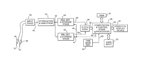
18 Turning now to Fig. 5 of the dldwing, which is a simplified block diagram
19 illustrating an embodiment of the present invention, the device is shown to be com~lised of
an input stage 20, an attenuation and gain stage æ, a signal m~ximllm detection and storage
21 stage 24, a signal miniml-m detection and storage stage 26, an analog-to-digital coll~ ion
22 stage 28, a colll~uldtion and control stage 30 (microplocessor), a random access memory
23 (RAM) 31, a means for user input 33, a graphical display device 32, and a time base
24 reference generator 34. As in other related types of metering devices, a pair of test probes
36 and 38 are provided having suitable conta~-ting tips, clips or transducers 35 and 37 for
26 eng~ging selected points in a circuit to be tested such that a voltage dirfelelllial appears
27 across the selected points, evidencing the current flow or potential levels to be detected or
28 monitored. The probes 36 and 38 can be of any suitable configuration, and normally probe
39822 U.S. Patenl Applicalion -- Page 6 54213 0047
' _ ~ 21g69~1 (
36 would be considered the positive or hot probe while probe 38 might be considered the
2 common or ground probe.
3 Input stage 20 interacts with the probes 36 and 38 to develop a signal at 40 which
4 is an analog of the voltage dirrer~llce sensed between the probe contact points. Signal 40
is then passed through att~ tion and gain stage 22 wlle~hl its signal level is adjusted up
6 or down so as to be compatible with the rem~ining circuit elements. The enh~nrecl signal
7 is then output on line 42 for input to maximum detector 24 and minimum detector 26, which
8 detect the V,r" ,~ and Vmjn for output on lines 48 and 50 respectively. These analog signals
9 are then coupled into the analog-to-digital converter 28 where they are 1igiti7~d and output
on bus 52. Colll~ulalion and control stage (microprocessor) 30 then causes the signal values
11 to be stored in RAM 31. Microprocessor 30 subsequently reads out the stored values and
12 generates signals on bus 54 for driving the graphical display device 22. Microprocessor 30
13 also periodically generates reset signals on line 49 for input at 46 and 47 to reset the
14 detectors 24 and 26, thus causing them to output the m~ximllm and minimum signals to
analog-to-digital conveller 28 for conversion to digital signal values. The time base
16 lefe.ellce gellelator 34 provides a master clocking input at 60 to the micr~pr~cessor 30,
17 whereby the mic~ ,cessor ge~ les the reset signals periodically in accor~allce with user
18 input or in accordance with an interval that is a function of the period as ~letecte~l from the
19 input signals.
It will thus be appreciated that by detecting the m~ximllm and miniml-m signal values
21 occurring during pre-3et~ in~l time intervals P (or P') to genel~le Vma,~ and V""" for each
22 sample period, and then (ligiti7.ing and storing these values, such values can be subsequently
23 read out of RAM 31 (and shifted in time) at a selected rate and used to drive a display in
24 a histographic fashion such as is illustrated in Fig. 6, with each glitch being depicted in
readily perceivable form, as indicated at 62 and 64. By histographic display it is meant
26 that, by repetitively sampling and shifting the stored data, the illustrated signal can be made
27 to appear to move across the screen 66 from left to right, creating a display remini~cent of
28 a strip-chart recorder in which the recording medium is moving from left to right. By
29 highlighting the displayed signal range between Vn,;l,~ and Vmjn as indicated at 60, the
39822 U.S. Palent Applicalion -- Page 7 54213 0047
` -
219695~
h,ro~ ation content of the display can be enh~nr~. It is to be understood that other display
2 formats can be used as well to facilitate observations of the glitches.
3 The stored Vm"~ and Vmin may be manipulated in a variety of manners. For example,
4 the average of several consecutive sets of Vma,~ and Vmjn values may be taken and displayed,
or the highest and lowest values from the several consecutive sets may be taken and
6 displayed. Furthermore, the number of consecutive Vma,~ and Vmjn value sets taken for the
7 above calculations can be changed to vary the rate of display.
8 Turning now to Fig. 7, a s~-h~m~tic circuit diagram is provided illusLI~tillg a
9 plc;r~ ,d implem~tation of the m~ximum and minilllulll signal detection/storage stages 24
and 26. As depicted, the input on line 42 from the gain stage 22 (Fig. 5) is fed through a
11 buffer amplifier 70, a blocking diode 71, a diode-connected t dnsi~lor 72, and a current-
12 limiting resistor 74 to a storage capacitor 76 which charges up to and holds the m:.x;".l~
13 voltage input during t_e sampling period P. This voltage is then output to t~rmin~l 48
14 through a buffer amplifier 78, to be sampled by the A/D. At the end of each period P, the
stage is reset by a frame-reset signal 46 ge~ dted by microprocessor 30 (Fig. 5), which
16 turns on the analog switch 80 to disch~lge the capacitor 76 to the l1egalive power-supply
17 rail. Note that because diodes 71 and 72 prevent discharge of capacitor 76 back into
18 amplifier 70, the period P can extend over any number of cycles of the input signal (any
19 selected period of time) and is thus not d~ lin~1 by the type of input wave form.
Tracking diode 73 serves to cause the output signal 48 to respond faster to large input signal
21 changes by bypassing the storage capacitor 76.
22 The ,,,i~-i.--l-.,, detection/storage stage 26 includes a buffer amplifier 82, a blocking
23 diode 84, a tracking diode 85, a diode biased lld~si~L~l 86, a current limiting resistor 90,
24 and a storage capacitor 92. Stage 26 further includes means for resetting (~chaL~ g)
capacitor 92 through an analog switch 94, and a buffer amplifier 98 for coupling Vmin out
26 at S0. Stage 26 operates to capture on capacitor 92 the minimllm voltage excursion during
27 each sampled period of the wave form input at 42. Capacitor 92 is initially positively
28 charged (rather than negatively charged as in circuit 24) by the reset signal applied at 46,
29 and its charge is reduced by the signal input at 42. The corresponding Vmjn value is then
39822 U.S Paten( Apl)lication -- Page 8 54213 0047
2196951
output via buffer amplifier 98 at 50, and the stage 26 is reset by the frame-reset input from
2 the microprocessor on line 46.
3 The analog-to-digital collvelter 28 and the microprocessor stage 30 are of standard
4 configuration, and in the p,~Çe-l~d embodiment are respectively implçm~nted using a
ADC10158 converter m~mlfactllred by National Semiconductor and a M37451
6 microprocessor m~nllfactllred by Mitsubishi Electric. The graphical display device 32 in
7 the prere-.ed embodiment is an LCD display of the type made by Seiko Instruments.
8 As actually implem~nt~l, the present invention forms part of a graphing, digital
9 mllltim~ter and ~ nostic ~l~t~b~e instrument m~mlfactllred by Balco, a division of Snap-on
Incorporated. It will be appreciated, however, that the invention could be embodied as a
11 stand-alone unit or as a component part of another in(licator or diagnostic system.
12 Furthermore, although the present invention has been described above in terms of
13 a specific embodiment, it is anticipated that alterations and modifications thereof will no
14 doubt become app~e--l to those skilled in the art. It is therefor~ int~ntled that the following
claims be i.lt~ eted as covering all such alterations and modifications as fall within the true
16 spirit and scope of the invention.
17 What is claimed is:
39822 U.S. Pa~rl Applica~ion -- Page 9 54213 0047