Note: Descriptions are shown in the official language in which they were submitted.
CA 02197048 2003-12-05
68086-681
-1-
A TURBINE ENGINE IGNTTION EXCITER CIRCUIT
INCLUDING LOW VOLTAGE LOCKOUT CONTROL
RELATED APPLICATION
This application corresponds to a continuation-in-part of U.S. Application
Serial No. 081207,717 filed on March 9, 1994 entitled "A Turbine Engine
Ignition
Exciter Circuit".
BACKGROUND
The present invention relates generally to high voltage power supplies and,
more specifically, to an improved ignition exciter for turbine engine
applications.
Turbine engine ignition exciters have evolved considerably since their
inception in the 1950's. First generation ignition exciters incorporated
vacuum tube
spark gap switching devices and vibrator type chopper, or DC-DC converter
circuits.
Given the severe operating environment of a turbine engine, e.g. high
vibration,
temperature extremes and widely varying input voltage and load impedance
conditions, considerable effort was expended to develop highly reliable first
generation components and circuit configurations. First generation exciters
provided
no way for aircraft or engine control, or feedback from the igniter plug to
the exciter
circuitry. Subsequently units ran open-loop. Following the introduction of the
EEC
(electronic engine control) computer and subsequent decline in former hydro-
mechanical engine control devices, second generation ignition exciter
circuitry
developed.
Second generation ignition exciters were typically characterized by
replacement
of spark gap switching technology with a semiconductor switching device. These
exciters commonly utilized three terminal (thyristor) switching devices to
accomplish
switching. This technology offered more precise spark timing and communication
with an electronic engine control computer since feedback information could be
effectively processed by the exciter charge pump (DC-DC converter) section.
This
provided a significant improvement over first generation devices, affording
aviators
considerably more control over. the engine ignition process.
' 006523-292
2197048
-2-
Conventional solid state ignition exciter circuits generally fall into one of
two
distinct categories. The first category being characterized by a series stack
of
switching devices to evenly distribute or divide the high (approximately 2-4
kV) tank
capacitor voltage across each device. Such exciters incorporate elaborate
voltage
divider networks to protect the series ganged semiconductor switching devices
from
electrical imbalances generated during both the capacitor charge and discharge
cycles.
During the capacitor charge cycle, voltage must be evenly distributed across
each
device to prevent catastrophic failure of the entire series ganged
semiconductor
switching network. Likewise, during the discharge cycle, a series ganged back
bias
diode network is required to protect the switching devices from ring back
which
results during igniter plug firing. Circuits using this type of circuitry
require careful
screening and matching of thyristor leakage current and similar
characteristics to
ensure proper operation at elevated ambient temperatures. Moreover, this
technology
is electrically inefficient since the combined losses of several individual
switching
elements (during on-state) are very high.
By contrast, a second current circuit design philosophy incorporates a single
thyristor switching device operated at a comparatively lower (.4-1 kV) tank
voltage.
This approach offers considerably higher efficiency than the first design
philosophy
since only a single (VI) loss is incurred rather than multiple losses
experienced with
the aforementioned series ganged approach. However, this benefit is quickly
offset
since the tank capacitor voltage must be significantly lower than the series
ganged
approach to avoid using "hockey puc" type switching devices. While "hockey
puc"
type switches would offer adequate voltage ratings, their considerable bulk,
weight
and Limited di/dt capability preclude their use in pulse discharge type
circuitry.
Therefore, current designs tend to utilize roughly 1,500 volt rated (phase
control type)
thyristors with correspondingly lower tank voltage.
This approach has two primary drawbacks. First, tank capacitor volumetric
efficiency is generally low due to the low energy storage voltage (E='/aCV2).
To
reliably fire (ionize) low voltage, e.g., 2-3 kV, igniter plugs, exciters of
this type
employ pulse networks to boost the low (.4-1 kV) tank voltage to the necessary
igniter
ionization voltage. Consequently, exciter output ionization voltage is limited
to low
006523-292
2191048
-3-
voltage semiconductor igniter plug applications since losses incurred in the
exciter
discharge pulse forming network become excessive when high step-up transformer
ratios are used. Moreover, regardless of transformer ratio, the transformer
itself has
considerable inductance and a saturable core to protect the semiconductor
switching
device from high di/dt generated during pulse network charge period, thus
decreasing
transformer efficiency.
Increased transformer losses tend to limit exciter peak power/duration while
lowering overall electrical efficiency. Hence, ignition system performance is
compromised. When used with low voltage igniter plugs under extreme operating
conditions such as high combustor pressure, water or fuel fouling, ionization
energy
(pulse) provided by the exciter pulse network may be insufficient to properly
ionize
igniter plug resulting in a quenched condition. To alleviate this problem,
larger pulse
transformers can be employed which increase pulse duration, however, at the
expense
of exciter volume/weight performance. Realistically, a point is reached where
pulse
network technology cannot overcome quench losses, since output PFN pulse
duration
is on the order of several microseconds and a quenched igniter can require
(ionization)
input voltage waveforms on the order of several hundred microseconds before
sufficient charge is accumulated to ionize the igniter plug gap.
To date, both types of solid state semiconductor switch exciter circuits have
incorporated off the-shelf, commercially available, phase control type
thyristors.
These devices, while readily available in commercial markets, are designed
primarily
for 60 Hz power control applications. Consequently, the dv/dt and di/dt
ratings of
these devices is limited with respect to requirements of a pulse power
discharge
application. The following summary provides a background of various thyristor
technologies conventionally available for switch exciter circuits.
Phase-Control Thyristors are designed to maximize the silicon for use as
active
emitter area at 60 Hz AC. The devices have large, shorted emitters (for high
dv/dt)
with single-point center gates, and depend on the relatively slow plasma
spreading to
turn on emitter areas remote from the point center gate. Researchers have
extensively
examined the spreading velocity by viewing radiative recombination of the
plasma.
Despite comprehensive research, spreading resistance of conventional devices
006523-292
2~ 97048
._
necessitates low di/dt performance relative to turbine engine ignition exciter
requirements.
Inverter Thyristors have distributed or interdigitated gates (for high di/dt),
similar to transistor emitter patterns, to turn on and utilize larger initial
areas of the
emitter for faster turn-on. For faster turn-off, heavy gold or platinum
diffusion
and/or electron radiation reduce carrier lifetime, thereby reducing thyristor
turn-off
times (tq). Unlike transistors, inverter thyristors have heavily shorted
emitters to
prevent latch-up when dv/dt is being applied. These inverter design features
allow
thyristors to be used at high (up to 10 kHz) repetition rates, but at the
expense of high
forward voltage drop. High forward drop severely limits performance of these
devices in turbine ignition applications since increased (VI) power loss
accelerates
onset of thermal runaway, limiting upper temperature performance.
Gate Assist (GATO) and Gate Turn-Off (GTO) Th ristors have npn regions
which are designed like high-speed transistors, where the gate (or base) is
used for
charge-control functions. In GATO closing switches, the gate is used to
extract
charge from the gate emitter junction during the tq and dv/dt switching
interval. This
allows high rep-rate performance without the adverse on-state voltage trade-
off of
lifetime-controlled inverter SCR's. The disadvantage of GATO's is the
requirement
for negative gate bias and current during the off state and commutation
interval,
which considerably increases the complexity of exciter (thyristor) triggering
circuitry.
Gate Turn-Off Thyristors (GTO's) are similar to GATO's but must be lifetime
controlled to act as opening switches. GTO's are made with both symmetric and
asymmetric structures. Asymmetric GTO's are made both with and without anode
shorts. The best turn-off gains for GTO's are obtained with shorted anode,
asymmetric structures. So far, some of the highest di/dt pulse power closing
switches
have been GTO-type structures. These GTO emitter structures are ideally suited
to
receive and distribute high turn-on gating currents. If opening is not
required, the
highest possible hole-electron lifetimes will lead to the lowest possible on-
state
voltage. Therefore, GATO is perhaps the best conventional semiconductor switch
structure for pulse-power applications such as turbine engine ignition
systems.
006523-292
-' 2197048
-5-
MOS-Controlled Thyristors (MCT's) are integrated arrays of paralleled GTO
cells (on the order of 20 micron spacing), with complementary FET's connected
from
anode to gate and gate to cathode. All of the cells have turn-off FET's that
act as
gate cathode shunts during turnoff and during the off state. Some of the MCT
cells
have turn-on FET's connected from anode to gate. For those turn-on cells
having
their own anode-gate FET, the upper-base spreading resistance under the
emitter is
low, and good gate emitter injection is assured for good di/dt. However, not
all cells
have turn-on FET's and area utilization (60%) is not as good as with GATO's
( > 85 % ), precluding use of devices in volumetric/weight sensitive aviation
turbine
engine applications. Furthermore, MCT gate-yield considerations limit the
active area
to about 1 cm2. High-current high-voltage applications are therefore better
served by
GATO-type designs, even though the turn-off function is not required.
SUMMARY
Accordingly, it is an object of the invention to provide improved turbine
engine ignition exciter technology which allows volumetrically efficient,
lightweight,
and high reliability operation at ambient temperatures equal to, or exceeding
existing
ignition exciter designs. The present invention achieves these improvements
through
use of a specially designed Pulse Power Thyristor (PPT) semiconductor
switching
device. Turbine engine ignition exciters according to exemplary embodiments of
the
present invention are considerably different than conventional exciters since
multiple
series ganged, or single low voltage phase control type thyristor design
approaches are
replaced with a PPT thyristor specifically designed for pulse discharge
applications.
The PPT thyristor is constructed such that it is capable of nearly unlimited
di/dt, thus eliminating the need for specialized output Pulse Forming Networks
(PFN's) such as saturable reactors and the like. Moreover, by offering
extremely
high di/dt, at elevated temperature, while reliably blocking nominal 2-5 kV
tank
voltage, the PPT allows solid state exciters to utilize bona fide high
voltage, e.g.,
greater than 10 kV, PFN's. That is, the PPT can directly drive transformer-
capacitor
type pulse forming networks to achieve true high voltage output without damage
to
the PPT.
006523-292 --
2197048
-6-
According to one exemplary embodiment of the present invention, a
transformer-capacitor type PFN can be configured so that the pulse capacitor
is
charged by energy which is transferred from the tank capacitor upon triggering
of the
device. Alternatively, according to another exemplary embodiment of the
present
invention, a transformer-capacitor type PFN can be configured so that both the
pulse
capacitor and the tank capacitor charge simultaneously. This latter
configuration has
the added benefit of reducing stress on the pulse capacitor and creating a
more
efficient output because all of the tank capacitors stored energy is available
to the
output waveform created for the plug.
Another benefit, in addition to the ability to reliably tolerate high di/dt,
is the
ability of PPT based exciters according to exemplary embodiments to provide
higher
peak power (shorter spark duration). Ignition system peak power is known to
significantly improve engine light off performance when fuel is poorly
atomized,
whether through improper fuel control or ambient (low temperature) conditions.
The
present invention allows improved altitude re-light performance and reliable
ignition
of engines under such conditions through elimination of saturable reactor type
output
networks.
The pulse power thyristor based exciter, by virtue of, for example, its
ability
to directly switch relatively high ( > 2 kV) tank voltage, eliminates the
conventional
need for multiple thyristors and associated charging/back bias voltage divider
and
protection networks. Thus, exemplary embodiments of the present invention
offer
considerably higher reliability (through lower parts count) over a variety of
electrical
and environmental conditions since a single device is used for switching
rather than
multiple series ganged devices.
Likewise, the PPT switching device is a significant improvement over
conventional single thyristor exciters since it is specifically designed for
pulse
discharge applications. For example, the nominal (breakdown) voltage rating of
PPT
devices according to exemplary embodiments is greater than, for example, 5 kV.
Consequently, despite high (for example, 3-3.5 kV nominal) tank voltages,
reliable
circuit operation over the entire environmental and input voltage envelope can
be
achieved.
006523-292 -
2191048
It is another object of the present invention to offer improved electrical
discharge efficiency through use of a single pulse power thyristor type
switching
device rather than series ganged thyristors. Since a single semiconductor
switching
device is utilized, power dissipated across the exciter switching network is
minimized
to a single device voltage drop rather than multiple (typically 2-4) voltage
drops
associated with conventional series ganged designs.
Another feature of the present invention is protection against low input
voltages. Exciter circuits according to the present invention can, for
example, be
used in turbine engines of aircraft for ignition. In this exemplary
application, the
exciter circuit may be connected to a nominal 28 volt supply. However, due to
various circumstances, such as a reduced battery voltage due to, for example,
engine
starter drain or the like or adverse ambient conditions (e.g., high
temperatures), the
actual voltage delivered by the battery may be much less than its nominal
rating.
Under these circumstances, various elements of exciter circuitry according to
the
present invention may be subject to additional electrical or thermal stress,
e.g., fuses,
the charge pump (diode power supply) and switching components. According to
exemplary embodiments of the present invention, these adverse consequences are
prevented by rendering the circuitry inoperative when the input voltage
applied to the
circuitry drops below a predetermined threshold.
According to other exemplary embodiments of the present invention, an
alternative is provided to conventional techniques for operating exciter
circuitry. In
these conventional systems, exciter circuits were activated or deactivated by
selective
application of the input voltage. By way of contrast, Applicants' novel
exciter
circuitry provides constant application of input voltage to the exciter
circuitry and
instead provides control over activation of the exciter circuitry using a
signal line that,
for example, controls triggering of the PPT or the charge pump in the exciter
circuit.
This technique has, among other advantages, the benefit of reducing the amount
of
high gauge wiring necessary to configure the system in favor of smaller gauge
signal
wiring.
CA 02197048 2003-12-05
68086-681
-7a-
According to a further embodiment of the present
invention, there is provided a combination comprising: an
exciter circuit operable in a normal mode of operation to
apply a stored, stepped-up input voltage to an output device,
said exciter circuit including: a node for receiving an input
voltage; a voltage conversion device for stepping up the input
voltage; an energy storage device for storing the stepped-up
input voltage; and a switching device for outputting the
stored, stepped-up input voltage to said output device; and
l0 circuitry for preventing said exciter circuit from operating
in said normal mode of operation when said input voltage is
present and said circuitry determines that said input voltage
is less than a predetermined threshold voltage.
According to a further embodiment of the present
invention, there is provided an exciter circuit comprising:
a node for receiving an input voltage; a voltage conversion
device for stepping up the input voltage; an energy storage
device for storing the stepped-up input voltage; and a
semiconductor switching device for outputting the stored
voltage to a pulse-forming network; wherein said pulse
forming network comprises a pulse capacitor and a
transformer, said pulse capacitor connected to said voltage
conversion device so that said pulse capacitor is charged at
substantially the same time as said energy storage device.
According to a further embodiment of the present
invention, there is provided an exciter circuit comprising:
a node for receiving an input voltage; a voltage conversion
device for stepping up the input voltage; an energy storage
device for storing the stepped-up input voltage; a switching
device for outputting the stored, stepped-up input voltage
to an output network; and circuitry for selectively
disabling said voltage conversion device based on a control
signal from an external source, wherein said circuitry can
CA 02197048 2003-12-05
68086-681
-7b-
use the control signal to disable said voltage conversion
device independently of the stored, stepped-up input voltage
on said energy storage device.
According to a further embodiment of the present
invention, there is provided an exciter circuit comprising:
a node for receiving an input voltage; a voltage conversion
device for stepping up the input voltage to at least 2 kV;
an energy storage device for storing the stepped-up input
voltage; and a semiconductor switching device for outputting
the stored voltage to a pulse-forming network; wherein said
pulse forming network comprises a pulse capacitor and a
transformer, said transformer having a primary winding
inductance of less than 25 microhenrys.
According to a further embodiment of the present
invention, there is provided an exciter circuit comprising:
a node for receiving an input voltage; a voltage conversion
device for stepping up the input voltage; an energy storage
device for storing the stepped-up input voltage; a switching
device for outputting the stored, stepped-up input voltage
to an output network, said switching device having a di/dt
characteristic of at least 200 amperes per microsecond; and
wherein said output network comprises a pulse capacitor and
a transformer.
According to a further embodiment of the present
invention, there is provided an exciter circuit comprising:
a node for receiving an input voltage; a voltage conversion
device for stepping up the input voltage; an energy storage
device for storing the stepped-up input voltage; a
semiconductor switching device for outputting the stored,
stepped-up input voltage to an output network, and wherein
said output network comprises a peaking network including an
air core inductor and a capacitor.
006523-292
2197048
_g_
BRIEF DESCRIPTION OF THE DRAWINGS
The foregoing, and other, objects, features and advantages of the present
invention will be more readily understood upon reading the following detailed
description in conjunction with the drawings in which:
FIG. 1 is a block diagram of an exemplary ignition exciter assembly according
to the present invention including a Pulse Power Thyristor (PPT) and automated
feedback circuitry;
FIG. 2A is a comparison of a standard 60Hz phase control waveform with an
exemplary exciter discharge (pulse power) waveform from circuitry according to
the
present invention;
FIG. 2B is a graph illustrating waveforms generated using conventional
semiconductor switching technology;
FIG. 2C is a graph illustrating waveforms generated by an exemplary PPT
according to the present invention;
FIG. 2D is a graph comparing conventionally generated waveforms with
waveforms generated according to the present invention on a different time
scale;
FIGS. 3A-3B compare cathode/gate metalization area of a standard 1.5 kV
phase control thyristor with an exemplary PPT according to the present
invention;
FIG. 4 illustrates an exemplary PPT emitter/base region geometric
relationship, which allows immediate conduction of high (di/dt) current
following a
gate trigger pulse;
FIG. SA illustrates various exciter output Pulse Forming Networks (PFN)
which can be used according to exemplary embodiments of the present invention;
FIG. SB illustrates an exemplary implementation of a transformer-capacitor
PFN according to the present invention;
FIG. SC illustrates another exemplary implementation of a transformer-
capacitor PFN according to the present invention;
FIG. SD is a graph illustrating voltage across the pulse capacitor for the
exemplary implementation of FIG. SB;
FIG. SE is a graph illustrating voltage across the pulse capacitor for the
exemplary implementation of FIG. SC;
006523-292 w
2197048
-9-
FIG. 6 is a cross-sectional diagram of a PPT illustrating the edge bevel
region;
FIGS. 7A-7B illustrate different edge bevel (sand blasting) techniques and
methods according to the present invention;
FIG. 8 illustrates a conventional hockey puc thyristor edge beveling
technique;
FIGS. 9A-9B contain both schematic and isometric representations of an
emitter shorting technique according to the present invention used to increase
PPT
junction temperature (T~);
FIG. 10 provides a cross-sectional illustration of PPT asymmetric and integral
back bias edge bevel geometries according to an exemplary embodiment of the
present
invention;
FIG. 11 graphically depicts an exemplary (anode) P region carrier
concentration following ion implantation and diffusion of Al, Ga and B;
FIG. 12 illustrates an exemplary PPT cathode carrier concentration;
FIG. 13 is a continuation of the PPT cathode carrier concentration profile of
Fig. 12;
FIG. 14 provides a summary of an exemplary PPT (silicon) manufacturing
process according to the present invention;
FIG. 15 illustrates (in sheet rho versus etch time) an exemplary process used
to form the emitter structure according to the present invention;
FIGS. 16A-16D contain an exciter schematic circuit diagram of an exemplary
circuit embodiment, including PPT switching thyristor and feedback circuitry;
FIG. 17A is a graph illustrating conventional storage device charging time;
FIG. 17B is a graph illustrating storage device charging times according to
the
present invention under a first set of conditions;
FIG. 17C is a graph illustrating storage device charging times according to
the
present invention under a second set of conditions;
FIG. 17D is a modified portion of FIG. 16A used to describe an exemplary
embodiment of low voltage lockout circuitry according to the present
invention;
FIGS. 17E and 17F illustrate two exemplary embodiments of FADEC input
control circuit according to exemplary embodiments of the present invention;
006523-292
2197048
-10-
FIG. 18 presents an exemplary optoelectronically triggered embodiment of the
present invention;
FIG. 19 illustrates an exemplary microprocessor/controller based embodiment;
FIG. 20 illustrates an exemplary impulse generator which can be used as the
output PFN of exciter circuits according to the present invention;
FIG. 21 illustrates a cathode/gate metalization pattern of a PPT according to
another exemplary embodiment of the present invention;
FIG. 22 is a cross-sectional view taken across line A-A of FIG. 21 in an
equivalent circuit interpretation; and
FIG. 23 is a cross-sectional view taken across line B-B of FIG. 21.
DETAILED DESCRIPTION
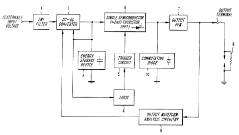
Referring to FIG. 1, block diagram operation is as follows. Input EMI filter 1
accepts input voltage from system level power supply. Filter 1 can be
configured in,
for example, either simple first order L-C, Pi, T, or common/differential mode
topology (depending on program requirements) to protect sensitive exciter
electronics,
and surrounding systems in close proximity to the exciter from
conducted/radiated
emissions/susceptibility. The EMI filter 1 commonly incorporates reverse
polarity
diode protection (not illustrated) to protect the exciter from inadvertent
application of
incorrect input polarity.
Filtered input power supplied to the DC-DC converter 2 is transformed to high
potential (on the order of, for example, 2-4 kV) for subsequent storage on
energy
storage device 3. Although this exemplary embodiment illustrates a DC input
power,
those skilled in the art will readily appreciate that an AC input power could
also be
used in conjunction with, for example, transformer rectification of the AC
input
power. To minimize effects of reflected load impedance on the input power
supply, a
flyback type converter arrangement is used. Unlike forward converters,
half/full
bridges and the like, flyback converters allow exciter circuitry to operate
over a wide
input voltage range (on the order of 10-40 Vdc), while maintaining constant
energy
storage device 3 (tank capacitor) voltage.
006523-292 - _
2197048
-11-
It will be appreciated by those skilled in the art, that when the exciter
circuit is
first activated, or has just discharged, the energy storage device (load)
approximates a
short circuit. Conversely, prior to discharge, energy storage device 3
approximates
an open circuit. Reflected impedance of this widely varying load is minimized
through use of, for example, flyback type DC-DC converter which effectively
isolates
input supply from tank capacitor load. The DC-DC converter can be configured
using both current and voltage control feedback loops to maximize power
transfer
e~ciency while minimizing heating within both magnetic components and
semiconductor switching devices.
As charge is incrementally imparted on energy storage device 3 (which can be,
for example, a tank capacitor such as a reconstituted mica capacitor), logic
circuitry 4
monitors tank capacitor voltage. When energy storage device 3 has reached full
charge, logic circuit 4 activates trigger circuit 5. The trigger circuitry may
include an
electromagnetic (transformer) coupling device or an optoelectronic coupling
device.
Regardless of the type of coupling used, trigger circuit 5 activates a single
high
voltage, di/dt thyristor switching device 6 allowing discharge of energy
stored in
energy storage device 3 to output PFN 7, and mating ignition lead (not
illustrated) and
igniter plug 8 (load) components. During discharge, the majority of energy
stored in
the energy storage device 3 is delivered to output PFN 7.
Following delivery of energy from energy storage device 3 to output PFN 7,
energy is subsequently recirculated from the load, through PFN 7 by
commutating
diode 10, creating a unipolar output waveform. This increases spark intensity
(heat
for given stored energy) since the waveform does not repeatedly cross zero,
creating
an oscillatory power waveform. Likewise, commutating diode 10 protects
switching
(PPT) thyristor 6 from stressful reverse bias transients which would occur
without the
commutating diode. Those skilled in the art will appreciate, however, that
commutating diode 10 can be omitted if unipolar output is not desired.
Exciter timing is accomplished by logic circuit 4. This circuit is constructed
from a stable multivibrator which may be constructed in a variety of ways, as
will
later be described with respect to Figures 16 and 19. Logic circuit 4 provides
a low
duty cycle, low frequency output waveform with the period of the output
waveform
006523-292 - -
2197048
-12-
being inverse to the exciter spark rate. During the steady state operating
case, logic
circuit 4 generates pulses at any desired low steady state spark rate. Due to
the low
duty cycle, DC-DC converter 2 is activated only periodically. This causes the
DC-DC converter to rapidly charge energy storage device 3, minimizing leakage
current and power dissipation through single semiconductor switching device 6.
During periods of extreme igniter plug fouling, combustor pressure, or wear,
igniter quenching may occur. To ensure igniter plug sparking occurs, the
output
waveform analysis circuit 11 can be provided to continuously monitor exciter
output
waveform (duration and amplitude), correcting output voltage, energy and spark
rate,
when igniter quenching occurs. By increasing exciter energy storage voltage,
output
voltage and energy are increased together as defined by E='h CVz. Likewise,
logic
circuit 4 is directed to increase charge pump frequency. By doing so, extreme
ionization voltage requirements of severely worn igniter plug gaps, and
dielectric
insulating influence of quench media, e.g. water, fuel or high combustor
pressure are
quickly overcome. By increasing exciter power output, quench media are quickly
dissipated. It will be recognized by those skilled in the art, that any or all
of the
aforementioned parameters can be controlled by output waveform analysis
circuitry 11
in a variety of different configurations. For example, circuitry can be
configured with
"time out" and manual override features to limit the amount of time that the
exciter
will attempt igniter "boost" operation and/or allow user override when a boost
function is not desired. This prevents excess ignition system stress and
allowing
maximum operating flexibility. Moreover, for those systems not requiring
diagnostics, waveform analysis circuitry 11 can be omitted.
The novel Pulse Power Thyristor (PPT) switching device, by virtue of its
unique design and construction, is capable of driving a variety of output
pulse forming
networks. The unique "double gate" PPT thyristor schematic symbol seen in
block 6
of Figure 1 is used to differentiate the PPT device from conventional
thyristor
devices. Double gate leads denote the considerable interdigitation of gate and
cathode
structures and associated high (di/dt) current carrying capability of
exemplary
embodiments of the PPT according to the present invention. Unlike conventional
phase control devices which are typically designed to handle comparably slow
rise
006523-292
2191048
-13-
time 60 Hz sinusoidal waveforms, exemplary PPTs are specifically designed to
reliably conduct pulse discharge waveforms.
FIG. 2A illustrates differences between 60 Hz sinusoidal 12 and typical
turbine
engine ignition discharge waveforms 13. Exciter discharge waveforms ideally
have
zero rise time, and durations on the order of 30-200 ~,s. Rise time is
important to
ensure reliable igniter ionization and exciter peak power. By contrast, a 60
Hz
waveform has a low dv/dt and di/dt (long rise time), on the order of 4 ms,
i.e., over
two orders of magnitude longer. Thus, it is not surprising that the structure
of
conventional thyristors is not ideal for pulse power applications as will be
discussed
below.
Figure 2B illustrates operation of a conventional semiconductor switching
device in a pulse discharge application. Waveform 270 represents the gate
drive
(capacitor voltage) of the conventional semiconductor switch. When the energy
storage device, i.e., capacitor, is charged to, for example, 80V, this voltage
is
discharged through the conventional semiconductor switch. This begins in
Figure 2B
at time equal to. Waveform 272 illustrates the anode-cathode current of the
conventional semiconductor switching device as a function of time. Note the
low
di/dt and considerable lag time before reaching peak current.
By comparison, Figure 2C illustrates PPT operation according to an exemplary
embodiment of the present invention. Waveform 280 is the PPT trigger capacitor
voltage as a function of time, with triggering again occurring at to. Waveform
282
shows the anode-cathode current for the exemplary PPT. Note the virtually
infinite
initial di/dt after triggering.
Figure 2D is provided as a more robust comparison using a different time
scale for clarity of the conventionally generated waveform 290 and a waveform
292
generated when an exemplary PPT is triggered. Note the very different di/dts,
i.e.,
about 580 A/~,S for waveform 292 versus 118 A/~cS for waveform 290.
FIGS. 3A and 3B illustrate differences in structure between traditional phase
control thyristor structures and the novel PPT device. It will be noted that
conventional phase control devices, generically illustrated in Fig. 3A, have
thin
intrinsic Si structures for limiting blocking voltage to <_ 1.5 kV and also
have
006523-292
2197048
-14-
essentially point contact gate regions 14 surrounded by the cathode region 15.
Conversely, the PPT (exemplified in Fig. 3B) utilizes interdigitated
gate/cathode
geometries 16 and 17. Note the relatively long gate/cathode periphery in
Figure 3B
as compared with that of Figure 3A. Interdigitation of the gate 16 and cathode
17
structures provides several important advantages relative to pulse discharge
(di/dt)
conduction. For example, when the device is triggered, gate charge is
immediately
distributed over the entire die face, thus eliminating plasma spreading
resistance time
delay. Likewise, the thick film, or solid metal cathode (comb) structure 17
more
efficiently collects charge during conduction, thereby eliminating excess
current
density during high di/dt periods. Hence, this extremely compact device, e.g.,
having
a package area of 1.5 in. by 1.75 in. or less, is well suited for the high
rise time,
di/dt waveforms associated with turbine engine ignition exciters. These
qualities
provide, among other advantages, for use of novel PFN configurations according
to
the present invention which were previously not possible using conventional
phase
control devices.
Referring to FIG. 4, unlike conventional thyristors, the PPT emitter and gate
geometries are such that the emitter center line is everywhere equidistant
from the
gate region, and less than a single diffusion length L from the gating region
400.
FIG. 4 also shows exemplary widths of the various layers for purposes of
illustration.
The emitter region width Y is maintained at, for example, less than or equal
to 10
times the gate (P base) region which, in this example, means that the emitter
width Y
is less than or equal to 0.06 inches. This ensures maximum use of the entire
emitter
area during initial triggering. That is, during application of a gate trigger
pulse, the
entire emitter region is activated preventing concentration of charge in
proximity of
the gate connection which occurs in conventional point contact thyristor
designs, i.e.,
gate 14 in Figure 3A. This feature allows the entire device to modulate and
conduct
full anode current coincidental with the application of a (gate) trigger
pulse. These
qualities also allow circuits according to exemplary embodiments of the
present
invention to easily accommodate a variety of output PFN topologies which was
not
possible using conventional (phase control) thyristor technology.
006523-292
2197048
-15-
FIG. SA illustrates several exemplary PFN's which can be used in exciter
circuits according to the present invention. Since the PPT single
semiconductor
switching device has practically unlimited di/dt capability, the need for a
saturable
output network 22, which was required in conventional exciter circuits having
semiconductor switches, is eliminated. For example, an air core output 18,
inductive
output 19, L-C peaking output 20 and bona fide high voltage, e.g., capacitor-
transformer networks 21, can be used in exciter circuits according to the
present
invention without di/dt or dv/dt failure. Moreover, exciters utilizing simple
L-C
peaking networks 20 operate with higher reliability since di/dt effects of the
resonant
peaking capacitors 210 do not adversely affect the PPT. Consequently, simple
air
core and peaking outputs 18 and 20 can be utilized with low voltage (e.g., 3-
10 k~
applications, increasing exciter peak power (reducing spark duration), thus
improving
ignition system performance.
As described above, conventional devices intentionally limited the di/dt
experienced by the semiconductor switch to avoid damage thereto. This was
accomplished by, for example, the inclusion of large (e.g., on the order of 10
mH)
saturable inductors in the output network connected to the switch. In addition
to other
drawbacks associated with using saturable inductors in this manner, the
enforced low
di/dt also reduces the magnetic coupling (i.e., efficiency in energy transfer)
of
transformers used in the PFNs of high tension applications to step-up the
input
voltage. To combat this problem in conventional exciters, large, bulky
transformers
can be used which both provide sufficient saturable inductance in their
primary
winding to protect conventional SCRs and adequately couple energy to the
output.
However, these large transformers create other problems in that the exciter
package
becomes heavier, bulkier and more expensive, which is commercially
undesirable.
Additionally, the greater the energy to be stored in the energy storage device
for a
given exciter design, the higher the primary inductance and the larger the
magnetic
material core size for transformers to both protect conventional semiconductor
switches and adequately couple energy to the output.
However, use of Applicants' novel PPT in exciter circuits, which can
withstand very high di/dt and, therefore, does not require protective
saturably
006523-292
2197048
-16-
inductive output circuits to initially delay di/dt, allows for a remarkable
reduction in
the size of the transformer. Both primary inductance and core size can be
reduced,
which in turn reduces the size and weight of the exciter package. Two
exemplary
PFNs which include a transformer to step up the input voltage are described
below.
FIG. SB illustrates one exemplary embodiment of a pulse forming network
utilizing a transformer T 1 and capacitor C2 combination. Therein, element C 1
is the
energy storage device 3 illustrated in Figure 1, and trigger circuit 5 and PPT
6
operate as described above. The operation of this circuit is as follows.
Initially, the
capacitor C 1 (energy storage device 3) is charged by the DC-DC converter 2
(not
shown in Figure SB) via diode D1. When the PPT6 is activated by trigger
circuit 5,
a portion of the energy stored in capacitor C1 is delivered to transformer Tl.
Since
the secondary load, e.g., a high tension igniter plug attached to Vo,
initially acts as an
open circuit, no energy is discharged through that path. However, a portion of
the
charge stored in capacitor Cl is provided to the pulse capacitor C2 via the
primary
winding of transformer T 1. Pulse capacitor C2 creates a pulse current through
the
flyback transformer action of transformer T1 which results in a high tension
output
voltage waveform. This output waveform is sufficient to ionize the igniter
plug gap,
allowing the remainder of the energy stored in capacitor C 1 to dissipated in
the spark
plasma formed between the contacts of the high tension igniter plug.
Figure SC illustrates an alternative exemplary topology for output PFN 7
utilizing a pulse capacitor C2 and transformer Tl combination. In this
alternative
exemplary embodiment, the system simultaneously charges the pulse capacitor C2
and
the capacitor C1. Pulse capacitor C2 is charged through the primary winding of
transformer T1 and safety resistor Rl. Thus, the DC-DC converter 2 provides
additional energy sufficient to charge both capacitors C1 and C2 at this time.
During
discharge, however, energy does not bleed from the capacitor C 1 into the
pulse
network as in the exemplary embodiment of Figure SB. Thus, the energy stored
in
pulse capacitor C2 is shunted through the PPT 6 and the primary winding of
transformer Tl resulting in a high tension output.
Note that in neither example provided above does the transformer T1
significantly delay the current rise (di/dt) experienced by the PPT 6. This is
due to
006523-292
2197048
-17-
the very low primary inductance relative to the amount of energy stored in the
energy
storage device 3. For example, given an exciter according to the present
invention
which stores more than 2 kV, e.g., approximately 3kV, in the energy storage
device
3, the primary winding of transformer T1 can be less than 25 microhenrys and
preferably less than 20 microhenrys, e.g., 15.6 microhenrys. Moreover, the
core
volume of transformer T1 can be less than 1.5 cubic inches and preferably less
than 1
cubic inch, e.g., 0.92 cubic inches. This combination of transformer
characteristics is
possible due to the very high di/dt which the PPT is capable of handling and
results in
a relatively small exciter package with excellent performance.
The topology described in Figure SC provides several benefits when compared
with that of Figure 5B. For example, the topology of Figure 5C reduces voltage
ring
back stress (i.e., amplitude oscillations of the stored voltage) on the pulse
capacitor
C2. This beneficial effect can be seen by comparing the waveform of Figure SD
(voltage across the pulse capacitor C2 for the configuration of Figure SB)
with the
waveform of Figure SE (voltage across the pulse capacitor for the
configuration of
Figure SC) and noting the lower amplitude oscillation for Figure SE vs. Figure
SD
(3.71kV vs. 4.92kV). Moreover, discharge efficiency is improved since the
energy
stored in tank capacitor C1 is not expended on the pulse network. This also
provides
a greater exciter output voltage since all of the energy in the tank capacitor
C 1 can be
used at the igniter plug.
FIG. 6 illustrates a PPT structure according to an exemplary embodiment of
the present invention. By positively beveling the PPT die at edge 23 so as to
"spread
out" electric field lines when the device is forward biased, rather than the
traditional
negative bevels (which tend to concentrate E field lines under a forward bias)
utilized
by most hockey puc type phase control devices, a number of advantages are
realized.
At the edge of the chip, a unique pnp structure 240 is created by etching off
the outer n+ region. Note that accordingly the N+ (cathode) region is not
embedded
in p-doped material. Since the (equivalent) npn transistor has been eliminated
from
the outermost regions, edge leakage current involves only the pnp structure.
Additional etching, to the n-region, further reduces edge leakage to np diode
levels by
avoiding both npn and pnp gains. Since leakage current in the vicinity of the
bevel
006523-292 --
2197048
-ls-
edge area 23 is higher than in other areas, design according to this exemplary
embodiment ensures that this surface leakage current will not be amplified by
npn/pnp
thyristor action.
The bevel edge area 23 has been beveled in a manner that results in "spreading
out" of the electric (field) potential lines 24 in the edge region 25. This
unique
positive beveling ensures bulk field breakdown since the surface electric
field is
spread out over a longer distance 26 than the bulk electric field, thereby
promoting
maximum theoretical (bulk) breakdown. To further reduce leakage current, all
edge
regions 27 outside of lines AA can be treated with electron radiation, further
reducing
pnp gain and associated leakage current.
The emitter n+p junction and pn- regions 300 can also be made light sensitive
by etching close to the pn- depletion regions. Triggering photons generate
hole-
electron pairs within these depletion regions resulting in injection from both
p+ and
n+ emitting regions 28 and 29. The device can thus be made sensitive to light
radiation 30 by a unique etch which is pervasive over the entire gate-emitter
length
and provides exposure of n+p junction 300. This allows optional optoelectronic
triggering as an alternative to electromagnetic triggering. The gate-emitter
area is
relatively great as compared to standard phase control thyristors because the
device is
extensively interdigitated. Due to considerably higher isolation achieved with
optoelectronic coupling, exciter circuitry and "up stream" supply electronics
are
further protected from thyristor failure modes and effects.
Referring to FIGS. 7A and 7B, PPT edge beveling techniques according to the
present invention are illustrated. The rounded region 31 of FIG. 7B can be
desirable
since cracks and fractures 32 of FIG. 7A caused during processing and handling
are
minimized by elimination of sharp edge 33. Cracks and chips contribute
significantly
to, and can cause failure of, semiconductors since high leakage current and
low
breakdown voltage result therefrom. FIG. 7A illustrates a sand blast method of
die
edge beveling wherein sand 34 is blasted from the bottom of chip (die) toward
the
top. FIG. 7B illustrates a second method of forming the bevel where the sharp
edges
33 are replaced by rounded edges 31. By inverting the direction of the sand
blast, a
blunt edge, less prone to cracking is accomplished. The sand blast profile 34
shown
006523-292
2191048
-19-
in FIG. 7B eliminates the sharp edge since the distribution of the profile is
such that
some of the sand contacts the edge to round it off.
By contrast, FIG. 8 illustrates the conventional bevels for large, e.g., ..-.3
kV
hockey puc type thyristors. Current thyristor structures use a double bevel
angle, one
negative 35, and one positive 36. Negative (Vbo) bevel 35 tends to concentrate
E
field lines when the device is forward biased (anode positive WRT cathode;
forward
blocking condition). This promotes dielectric breakdown at device surface
rather than
through (bulk) Si. Conversely, phase control devices (which typically must
block
voltage reliably bi-directionally (60 Hz sinusoid)) require a second
"positive" bevel to
protect the device during reverse (Prv) bias condition. That is, when
sinusoidal stress
reversed polarity occurs, positive bevel 36 (which would normally tend to
spread
(surface) E field concentration) actually concentrates the field near the
interface with
negative bevel 35, thereby protecting the device from same bulk breakdown
phenomenon.
In contrast, a single PPT positive bevel 23 allows the device to realize
(bulk)
Si breakdown equal to theoretical Si breakdown. In comparison, traditional
hockey
puc devices such as that illustrated in FIG. 8 can only achieve, for example,
80 % of
theoretical (bulk Si) breakdown voltage; and must utilize considerably more Si
and
wafer "real estate" .
These conventional devices have blocking voltages on the order of 3 kV and
require 2 X 0.2" or about 10 mm (linear, over entire dimeteral surface) of Si
be used
for beveling. The novel beveling methods in FIGS. 7A and 7B according to the
present invention require only about 2 X 0.032", or 1.6 mm Si for the bevel
area.
This feature provides economic fabrication of devices with diameters on the
order of,
for example, about 4-25 mm, which are capable of reliably blocking, for
example, 2
to6kV.
Referring to FIG. 9A, if both emitting injectors 37 and 38 of the PPT
thyristor
structure are shorted, the device blocks voltage like a diode. That is, by
effectively
shorting the p+n 37 and n+p 38 injecting junctions of the thyristor, npn and
pnp
gains are eliminated thereby reducing leakage current levels to those
associated with
diode structures and permitting high temperature (T~ >_ 175 °C)
operation.
006523-292
2197048
-20-
FIG. 9B provides an isometric rendering of this emitter shorting technique.
Anode shorting is accomplished by an etch down of the p region, e. g. , at
region 90,
allowing penetration of n+, as depicted with Re (shunt resistors) and
penetration of
upper n+ layer into the p region. One method of cathode shorting, similar to
the
technique used for the anode side, involves building etched "holes" 92 in the
lower
p+ region which penetrate adjacent n+ material. These processes permit
effective
shorting of the cathode and/or anode emitters at low level (blocking current
levels)
such as those experienced during the energy storage device charge cycle, yet
permits
high current triggering and conduction at high conduction levels, such as
those
experienced during exciter discharge. Effective low level shorting and high
level
triggering is illustrated in the novel double sided etch down structure
illustrated in
FIG. 10.
FIG. 10 illustrates a method according to an exemplary embodiment of the
present invention for shorting both anode and cathode regions of both
symmetric and
asymmetric structures to achieve high blocking temperature capability and/or
intrinsic
inverse parallel (back bias) diode. Anode shorting reduces leakage current
associated
with imperfect passivation of the bevel area. Leakage current contributes
considerably to exciter power losses during capacitor charge cycle. Likewise,
since
leakage current increases with temperature, exciter top-end operational
temperature
performance is limited. At high temperatures, thyristor leakage causes die
heating
which, if unchecked, will continue until catastrophic thermal runaway occurs.
Anode
shorting is accomplished by removing (either by grit blast or etch method, for
example) the outer region 39 of the (P+) anode.
This procedure provides at least two significant advantages. First, a shorting
metal such as Au-As 40 can be alloyed into the n- region making an efficient
inverse
diode 41. Second, by limiting application of anode metal to the outer
periphery etch
region, defined by zone 39, an efficient blocking diode structure is created
at the
outer periphery of the pnpn device. Thus, eliminating npn and pnp gain at the
beveled surface (i.e., low leakage current), and providing reverse blocking
voltage
capability (asymmetric case). Cathode shorting can be accomplished by
introducing
internal shorts 43 over the entire emitter area or by providing external
resistors 44
006523-292
2191048
-21-
connected between cathode and gate terminals. This feature eliminates a
problem
associated with high temperature pnpn thyristor blocking voltage, i.e. pnpn
leakage
current is highest in vicinity of bevel area 45. Accordingly, Figure 10
illustrates how
the outer bevel area can be modified to eliminate pnp and npn gain due to
leakage
current along surface of bevel for both symmetric and asymmetric thyristor
structures.
It will be appreciated by those familiar v~th semiconductor processing, that
an
asymmetric thyristor device would contain an additional n+ layer 46, allowing
good
ohmic contact using Al or similar metalization.
FIGS. 11-15 illustrate an exemplary manufacturing technique of the PPT
according to the present invention. Figure 11 illustrates the p region
resulting from a
diffusion of Al, Ga and B into both sides of a 37 miI thick Float Zoned Si
wafer
which was NTD (Nutron Transutated Doped) to approximately 10E13 (cm3). The
novel diffusion technique involves ion implanting and driving Al, Ga and B
into the
wafer with an approximately 16 hour 1275°C diffusion cycle. To prevent
device
contamination, and associated excess leakage current, the Si is "capped" with
layers
of Si02-Si3N4-Si02 thus preventing entrance of contaminants and outdiffusion.
The
capping/oxide layer materials and order of application were developed to
provide a
complete "cocoon" around the Si wafer, preventing entrance of contaminants or
out
diffusion.
Likewise, the oxide layers have been optimized to prevent cracking of the
capping layer. It will be appreciated that the invention utilizes an ion
implantation
technique whereby Al, Ga and B are ion implanted through the oxide layer. A1
is
used to achieve a deep (approximately 4 mil) junction for high voltage
capability, with
a reasonable (approximately 16 hour 1275°C) diffusion. Due to the poor
(approximately 4 % ) electrical affectivity of Al, Ga and B are introduced to
increase
concentration of active electrical acceptors for good ohmic contact and
injection
efficiency. By way of contrast, conventional technology requires very long,
high
temperature diffusions, for example, about 135 hours at 1275°C, which
are
consequently prone to contamination from impurities, e.g. Na, which diffuses
through
(quartz) diffusion tubes increasing leakage current.
006523-292
2197048
-22-
To expand on this three element doping procedure, Al is used since it is a
fast
diffusing (P type) dopant which will dope an Si lattice properly with 16 hr.
1250°C
diffusion, as opposed to traditional B 135 hr. 1275°C diffusion. Al is
a good fit in Si
crystal, yielding low crystal stress. Unfortunately, Al tends to bond with
oxides
creating oxide complexes lowering the effective doping to roughly 4 % . Ga is
used
next to achieve higher doping concentration. Since Ga does not tend to form
oxide
complexes, it is a more e~cient dopant. Again, diffusion time is short.
Finally, B is
used as a getter to "lift" impurities to the surface where they can be removed
(etched
ofd. Boron also provides improved ohmic contact. Ion implantation through
oxide
layer prevents out-diffusion and prevents contamination by, for example, Na,
which
would reduce carrier lifetime and increase leakage current.
Exemplary embodiments of the present invention can utilize, for example,
either diffusion or microwave oven dopant drive technology. The microwave
technique can be implemented, for example, by replacing a standard fixed
frequency
magnetron with a variable frequency TWT (Traveling Wave Tube). This technique
is
favored since the TWT allows uniform RF heating of the Si, without heating the
surrounding environment, thereby significantly reducing probability of
contamination.
This is a considerable advancement over current diffusion oven techniques
since
diffusion temperature can now approach Si melting temperature. Diffusion oven
techniques are notably limited since quartz holding tubes used during the
diffusion
process are prone to sagging and devitrification at temperatures above
1200°C. The
resulting pnp structure is then one side lapped to a p concentration on the
order of
10E17. The wafer is then diffused with phosphorous, on both sides, to a depth
of
about, for example, 6.5 microns to form a npnpn structure as illustrated in
FIG. 12.
The anode n side is then removed forming the raw npnp wafer. FIGS. 11-13
illustrate the complete profile which is capable of blocking, for example, > 5
kV.
FIG. 14 illustrates an exemplary method of forming the Si surface, i.e.,
defining the emitter, through the metalization process. The starting Si
substrate is
made by the sequential diffusion of Al, Ga and B into a, for example, 450 Ohm-
cm,
37 mil NTD doped n- water thereby forming a pnp. One side of the wafer is
lapped,
etched and n+ phosphorus (POCL3) is predeposited and annealed to form a n+ pnp
006523-292
2197048
-23-
n+ wafer. The anode side n+ is then removed by etching forming the n+ pnp
structure.
Figure 14 depicts a process that enables construction of a high voltage PPT
type device that replaces planar diffusion fabrication methods, thus
eliminating carrier
lifetime reducing oxide mask/etch processes. That is, this process allows the
thyristor
to be etched, defined and metalized without any carrier lifetime reducing
process
steps, translating into lower on state (forward conduction) voltage. Although
the
Figure 14 process depicts only one sided processing, exemplary embodiments of
the
present invention can be realized by applying the teachings of Figure 14 to
both sides
of the wafer.
First, a low pressure chemical vapor deposited (LPCVD) nitride is deposited
and patterned through use of standard photolithography masking techniques.
Although
Figure 14 shows only one side being processed, the double sided shorting
depicted in
Figure 9 can be obtained, for example, by applying the process shown in Figure
14 to
both sides of the wafer.
The etch process described in Step 7 (FIG. 14) can be accomplished by
utilizing the selective etch process depicted in FIG. 15, and results in an
emitter step
height on the order of, for example, about 7.5 microns. The N+ etch down
procedure illustrated in FIG. 15, as opposed to the planar process used to
produce
conventional hockey puc devices (FIG. 8), renders the N+ (cathode) region
fully
exposed. This significantly increases optoelectronic qualities of device,
while
indirectly improving carrier lifetime. Since the N+ etch is a unique,
selective etch,
only N+ material is removed. The knee 150 on "square legend" curve of FIG. 15
illustrates the principle. That is, the etch down rate abruptly changes (slows
down)
when N + material has been removed, exposing underlying P material. This
provides
excellent uniformity and control which in turn allow the fine geometrics and
uniform
electrical performance of exemplary PPTs. Since the etch is selective, an
(Si02)
oxide layer is not required to protect P material. The oxide layer used in
fabrication
of standard devices reduces carrier lifetime, increasing on state (forward
conduction)
voltage. Also shown in Figure 15 is the increase in sheet resistance as the NP
junction is approached.
006523-292
2197048
-24-
Step 8 involves a non-selective Si etch that removes the remaining n material
to allow reliable contact to the p gate region; followed by the removal of the
nitride
mask (9). Steps 10-21 involve the metalization process which is also used to
alloy
dope the gate regions for good ohmic contacts to the lightly doped gate
regions. Al,
Ti, and Ni are evaporated onto the emitter side and etch separated to obtain
the gate-
emitter lateral diode. Step 20 involves anode metalization using blanket Al-Ti-
Ni. A
result achieved using this process is to obtain good ohmic contacts to both
lightly
doped p Si (the gate region), the heavily doped P anode and the n+ cathode.
God
on-stage voltage is then achieved by alloying the Al into the Si with SOOC
sinter step
21.
The foregoing describes how a high voltage, high di/dt and high temperature
thyristor can be made compactly, relative to conventional hockey puc (phase
control)
type devices. Now an exemplary application of this device will be described.
FIGS. 16A-16D illustrate a turbine engine ignition exciter circuit featuring
the
novel PPT switching device and automated feedback feature. For clarity, the
circuit
has been divided into four (4) major functional blocks: EMI filter, diode
converter
charge pump, energy storage and switching and diagnostic section. DC input
power
is applied between VIT and VI RTN terminals. Power is then fed through the EMI
input filter consisting of Ll, C1, C2, C3, L2 and L3. The EMI filter is
configured to
reduce common mode noise as well as differential mode signals which are
generated
outside the exciter. The filter also filters noise signals generated within
the exciter
system, preventing both conducted and radiated emission outside of the exciter
housing. In the case of radiated emission, the exciter is generally
constructed such
that either a separate metallic sub-enclosure, or PC board with considerable
ground
plane area is utilized to trap signals, preventing radiation. It should be
noted the
common/differential mode filter illustrated in Fig. 16A is just an example of
one of a
variety of viable circuit topologies which may be incorporated. Rectifier D1
serves as
a reverse polarity protection diode which protects the exciter from
inadvertent
connection of the improper input voltage polarity between terminals VIT and
VI RTN. Z1 is a zener over voltage transient suppression diode. The zener
diode is
used to suppress voltage transients present on the input power cable, such as
those
006523-292
2197048
-25-
induced during a lighting strike or aircraft/engine EEC switching. The zener
may be
replaced with a metal oxide varistor (MOV) or similar structure to accomplish
this
function, depending on specific program and design requirements.
Next, the diode converter charge pump will be described. F1 is a fuse
designed to protect the DC source in the advent of a catastrophic failure,
e.g. a short
circuited switching FET (Ql) within the exciter. Other combinations of
operational
parameters can also cause fuse F1 to blow as described below with respect to
Figures
17A-17C. Integrated circuits U1 and U5, in conjunction with corresponding
filter
capacitors C4, CS and C 14, C 13 form linear voltage regulator networks which
supply
a highly regulated voltage, of appropriate potential to the CMOS and linear
circuits
within the exciter circuit. C6 is a high capacitance storage capacitor which
forms part
of the filter network and provides an energy reservoir to T1 thus reducing
input
current spikes and EMI noise. Rl, C8, C9 and Z2 provide a stable reference
voltage
for the charge pump comparator U4A and tank voltage comparator U4B. U2
(Oscillator), R3, R4, (NPO capacitor) C10, R5, R6, Q3 and Q4 form an ultra
stable
oscillator which establishes the charge pump oscillating frequency and
determines the
spark rate of the exciter. The IC oscillator frequency is controlled by R4, RS
and
C10. Values are selected to achieve maximum switching frequency to reduce
component size.
The IC contains "divide-by-n" circuitry which allows stable high frequency
oscillator frequency to be divided, establishing exciter spark rate frequency.
It will be
appreciated that this method ensures extremely stable spark rate frequency
over entire
input voltage and environmental operating envelope. Transistors Q3 and Q4,
which
are controlled by the diagnostic feedback circuitry, adjust the oscillator
frequency
allowing momentary transition into a burst mode (high frequency spark rate),
when
igniter plug quench condition is detected. U3A (Flip-Flop), Q2, U4A
(Comparator)
and R41 form the heart of the charge pump circuit. U2 provides a (spark rate
frequency) clock signal to U3B which in turn activates U3A, turning on the
charge
pump at the (high frequency oscillator) clock rate set in U2. The Q output of
U3A
turns Q2 "off", thus activating Q1, ensuring proper (saturating) gate drive.
006523-292
2197048
-26-
As Q1 is activated, current begins to increase linearly through power
transformer Tl until the voltage across R12 (sense resistor) reaches the
comparator
U4A reference voltage as determined by voltage divider R8, R9. When the
comparator U4A triggers, U3A is reset turning off Q1 via Q2, thus establishing
a
current mode feedback control loop. This process continues in response to
consecutive U2 (high frequency) clock pulses until U4B, the voltage mode
comparator, resets the spark rate control "Flip-Flop" U3A.
For clarity R41 and R7 are "pull-up" resistors for the "open collector"
comparators outputs of U3A and U3B. R2 is an active pull-up for Q2 which
provides
drive to Q1. Z3 is a zener, which limits Q1 gate voltage to a safe value.
Power
transformer Tl is configured in a flyback configuration to minimize reflected
load
impedance and allow maximum output voltage over a widely varying input voltage
range. Transformer T1 contains a tertiary, or feedback, winding to fully
isolate the
(voltage) feedback loop signal level electronics from high voltage present on
secondary (tank capacitor) winding. When U3A causes Ql to open (via Q2), the
magnetic field contained in the core of Tl collapses. Due to phase
relationship of T1
windings and orientation of D2, energy stored in T1 is subsequently imparted
on tank
capacitor C 15. As charge incrementally accumulates on the tank capacitor, its
voltage
increases.
Dual FET's (Q1/Q2) can be used to prevent main switching FET Q1 from
operating in linear region at low (exciter) input voltages. At low voltages,
CMOS
driver (U3A) may not supply sufficient gate drive (voltage) to fully activate
Q1.
Therefore, Q2 can be used in a quasi-darlington configuration to ensure
maximum Q1
gate drive (di/dt). Z3 zener diode is used to protect Q2 drain-source junction
during
T1 flyback; clamp Q1 gate drive to save level.
Tank capacitor C15 is charged to the appropriate voltage (e.g., between
2-5 k~, through indirect action of the tertiary (feedback) winding on T1. The
network comprised of diode D4, R14, R15, R16 and C16, C17 produces a stable
(filtered) waveform which mirrors voltage present on C 15. When voltage on
tertiary
(feedback) circuit reaches set point of U4B (comparator), the comparator
output
toggles, resetting U3B (Flip Flop), turning off the charge pump (through U3A).
006523-292
2191048
-27-
Simultaneously, U3B (Flip Flop) activates Q5. Energy stored in C17 is then
discharged through trigger transformer T2, QS to ground. Trigger transformer
T2
generates a high voltage/current pulse which triggers the PPT (Pulse Power
Thyristor)
allowing energy stored in tank capacitor C 15 to flow through PFN to the
igniter plug
load. Diode DS serves as a recirculation diode for T7, protecting QS from
induced
(back) EMF.
For purposes of illustration only, a simple air core inductive output L4 is
depicted. However, those skilled in the art will appreciate that any of the
output PFN
(Pulse Forming networks) defined in Fig. 5 (including air core, simple
inductive, L-C
peaking and transformer-capacitor pulse networks) may be used reliably, over
the
entire exciter operating envelope without limitation due to the unique high
voltage,
di/dt capability of the PPT. Other PFNs can also be used; for example, the
impulse
generator described below with respect to FIG. 20.
Energy delivered to output inductor L4 is then delivered to the mating
ignition
lead and igniter plug load (not illustrated). The simple air core inductor L4,
in this
case, is used to adjust spark plasma discharge duration and peak power. This
feature
allows the exciter output to be precisely matched (tuned) to specific engine
requirements and achieve maximum ignition performance. This is a significant
advancement over conventional solid state exciter technology which must
intentionally
maximize exciter output duration, to minimize di/dt stress experienced by
phase
control type thyristor switching devices.
As energy begins to dissipate in the (igniter plug) load, D6, the unipolarity,
or
commutating diode provides a return path for discharge current. This diode
causes
current to recirculate through the load, D6 and L4 until energy is completely
expended. Back bias diode D3 provides a shunt path across the PPT for reverse
currents generated immediately following PPT conduction, thus protecting the
PPT
when it enters the reverse recovery mode. Leads to diode D3 are illustrated in
hidden
lines since back bias diode D3 can be made integral to the PPT as shown in
FIG. 10.
Resistors R17 and R18 form a voltage divider which samples a portion of the
output
voltage and supplies it to the diagnostic circuit 166 for processing.
Capacitors C18
and C 19 block the high voltage do present in the tank circuit, isolating
sensitive "front
006523-292
2197048
-28-
end" processing circuitry form high voltage dc, allowing only the AC dynamic
content
to pass. Resistor R13 is a safety resistor which discharges C15 following
removal of
input power.
Diagnostic signal processing is accomplished as follows. Signal input derived
from the R17, R18 C 18, C 19 AC voltage divider circuit is applied to the
diagnostic
inputs of (comparators) U13A and U13B. Both comparators are set to measure the
minimum output voltage of the exciter. U9, the diagnostic master clock
(oscillator),
provides one-shot timers U10 and U11 basic timing information for pulse
duration and
spark rate, respectively. One-shot U10 measures the time the exciter's output
voltage
waveform is above the comparator U1 minimum set point, established by
resistors
R34 and R35. When the exciter fires, the output voltage amplitude will quickly
diminish to the igniter spark plasma sustaining voltage (e.g., =50 ~ within
several
microseconds if the igniter plug is not quenched.
By contrast, when the igniter plug is quenched, output voltage will remain
high, nearly equivalent to tank voltage for many milliseconds. Due to the vast
(several orders of magnitude) difference in discharge voltage waveform,
igniter plug
quench condition is easily deduced. Therefore, U10 which is configured as a
time out
timer, generates a logic 1 output in response to the detection of a quenched
igniter or
an open circuit (lead). This logic 1 (from U10) is sent to U8A and UBB. U8A is
configured as a retriggerable "one shot" providing a fixed output pulse to
U12, a
digitally controlled potentiometer. Each time U12 receives a pulse for UBA,
the
potentiometer value is incremented (one step). The U12 potentiometer forms
half of
the tank capacitor comparator (U4B) set point voltage divider network.
Consequently,
each time the potentiometer is incremented, the tank capacitor voltage is
increased.
Increased stored energy increases probability of igniter firing. Increased
exciter tank
voltage causes stored energy to increase through E='h CVz. Each time the
igniter
fails to "fire" exciter output voltage and energy are incrementally increased.
During plug quench, U10 simultaneously supplies the (same) logic 1 signal to
UBB. Like UBA, U8B is also configured as a retriggerable "one-shot". Based on
component values of R26 and C29, U8B output pulse duration can be "programmed"
.
When U8B output goes high (Logic 1), the exciter charge pump (DC-DC converter)
006523-292
2197048
-29-
enters a "burst mode", which causes the exciter to transition from a low
steady state,
maintenance spark rate mode to a high spark rate burst mode. The combined
effects
of increased spark rate, ionization voltage and delivered energy are intended
to
overcome plug wear and fouling. If the igniter plug fails to fire following
each
exciter discharge, tank voltage and stored energy are incrementally increased
to the
limit of U 12. Likewise, depending on the "time out" value (determined by R26
and
C29), exciter charge pump will remain in high spark rate mode, as controlled
by
UBB, until the plug fires.
When the plug fires, U8B is reset, returning exciter to maintenance (steady
state) low spark rate mode. U7 is a counter which keeps track of the digital
potentiometer U12 "position". If the igniter does not fire after the digital
potentiometer, U12 has increased exciter output to maximum voltage/energy, U7
generates a logic 1 output which is supplied to U6B input. U6B is configured
as a
latch. When logic 1 is received from U6B, output latches causing FET Q3 to
close,
tying the "Fail Igniter" line to ground. The Fail Igniter line is subsequently
read by
an engine EEC or similar device to determine whether a quenched igniter or
open
circuit ignition system fault exists. Exciter output voltage and spark rate
analysis is
accomplished by action of comparator U13B and subsequent circuitry.
Output of U13B toggles each time exciter discharge occurs and exciter output
voltage signal provided by output AC divider circuit (R17, R18, C18 and C19)
exceeds the U13B setpoint value. This setpoint value is determined by resistor
divider network comprised of R37 and R38. The network comprised of U13B, U11,
U6A and associated support circuitry determines exciter output voltage and
spark rate
are within threshold limits. When U11, which is configured as a "time-out"
timer,
fails to receive a reset pulse from U13B before the (spark rate) time out is
reached, a
logic 1 output is generated, indicating low exciter spark rate. The logic 1
signal is
subsequently sent to U6A, which is configured as a latch. U6A then causes Q7
to tie
the "Exciter Fail" line to ground providing an EEC or similar system analysis
circuitry with an indication that annunciation exciter (low spark rate) fault
has
occurred.
006523-292
2191048
-30-
Similarly, when an input signal provided by exciter AC coupled divider
network fails to exceed the U13B setpoint value, Ull again times out,
providing logic
1 to U6A. In this case, the "Exciter Fault" line is again pulled low by Q7,
indicating
an exciter (low output voltage) fault.
Circuitry comprised of FET Q8, R24, R25 and C28 provides a reset signal to
U6 (A and B) when power is applied to the diagnostic circuit, resetting the
diagnostic
function. The circuit comprised of FET Q9 R29, R30, R31, R32 and C35 generates
a
"write" timing signal to U12 digital potentiometer. This "write" signal causes
U12 to
write the potentiometer setting to internal EEPROM circuitry, allowing the
exciter to
retain current output voltage and energy settings following removal of input
power.
By retaining settings, exciter output continually adjusts to changing engine
and igniter
plug wear conditions. The combined effects of the automated feedback and
diagnostics reporting circuitry allow exciter to automatically compensate for
changing
engine and system wear variables, advising the pilot or EEC system of system
wear,
and subsequent corrective action, extending useful life of the ignition prior
to actual
system fault and "catastrophic" failure reporting.
According to exemplary embodiments of the present invention, charge and
discharge cycles have been optimized to reduce stress on the PPT 6. For
example, by
charging and discharging the storage capacitor relatively rapidly, the PPT 6
need
block the stored voltage for less time, thereby placing less stress on the
semiconductor
switch. This concept is illustrated by the graphs of FIG. 17A-C wherein the
graph of
FIG. 17A illustrates conventional charging techniques which typically charge
an
energy storage device over a relatively long period of time. By way of
contrast,
systems according to the present invention charge the energy storage device in
significantly shorter periods of time as illustrated in the graphs of FIGS.
17B and
17C.
Unfortunately, there may be various conditions which necessitate an increased
charge time. This situation is graphically portrayed by the longer charging
times of
FIG. 17C relative to FIG. 17B. For example, as temperature increases, leakage
through the PPT 6 also increases which dissipates power and increases the
charge
time for energy storage device 3. Another factor which can lead to increased
006523-292
2197048
-31-
charging time is if the voltage input to the exciter circuitry is reduced. For
example,
there may be period of time, e. g. , at startup or when the battery supplying
power to
the system is low, when the actual voltage input to the exciter circuitry may
be much
lower than the nominal rating of that voltage. For example, the graph of FIG.
17B
may represent charging times at 25°C with the battery supplying 28 Vdc,
while the
graph of FIG. 17C may represent charging times for the same circuit operating
at an
ambient temperature of 121°C with the battery supplying 9 1/2 volts. In
a constant
power application, as the input voltage is decreased, the input current will
increase
along with the charging time for the storage capacitor due to Iz/R losses.
This has
several implications. For example, the fuse F1 illustrated in FIG. 16A which
protects
a circuit may blow if the input current increases beyond that at which the
fuse is
rated. Moreover, if the input voltage is low for a sufficiently long period of
time,
then the increased charging time may lead to a thermal runaway (breakdown) of
the
PPT 6.
In order to avoid the adverse consequences associated with lower than normal
input voltage, Applicants have developed a low voltage lockout feature which
prevents
the circuit from operating when the input voltage is lower than a
predetermined
threshold. The predetermined threshold can be selected to be any voltage level
which
is less than a desired operating input voltage depending upon various design
considerations. For example, for a nominal input voltage rating of 28 volts, a
threshold of 91h volts can be selected whereupon the circuitry will not
operate if the
input voltage drops below 9'h volts. An exemplary implementation of this low
voltage lockout feature will now be described with respect to Figure 17B.
In Figure 17B, the input voltage is monitored by comparator 234 through a
voltage divider comprised of resistors 8270 and 8280 and filtered by capacitor
C320.
A stable voltage reference is established by bias resistors 8250 and 8260,
zener diode
Z55 and filtered by capacitor C300. This voltage reference is then input to
the
inverting terminal of comparator 234. Resistors 8240 and 8230 provide a
comparator
hysteresis (e.g., approximately 0.3 V) which prevents oscillatory operation
when the
input voltage has a value which is approximately similar to that of the
reference
voltage applied at the inverting terminal of comparator 234. When the input
voltage
006523-292
2191048
-32-
applied at the non-inverting terminal of comparator 234 is less than that of
the
threshold voltage, then the Q output of flip-flop U3B through resistor 8220 is
shorted
and the current mode feedback loop controlled by flip-flop U3A is prevented
from
operating to actuate the trigger circuit.
Thus, when the input voltage is below specified limits, exciter operation is
inhibited because the primary (current mode) control loop is deactivated. This
prevents the charge pump from imparting charge (voltage) on the exciter tank
capacitor. In this way, the above-described problems that occur when input
voltage
droops and charge time increases are eliminated. In addition to restricting
the
operation of exciter circuits when the input voltage drops below a threshold,
other
exemplary embodiments provide a technique for activating and deactivating the
exciter
circuitry by way of an additional signalling circuit illustrated in Figure 17B
as
FADEC input control block 300. This feature will now be described with respect
to
Figures 17C and 17D.
Traditional exciters are activated and deactivated through application or
removal, respectively, of input power to the system. That is, with reference
to Figure
17B, to conventionally activate or deactivate the circuit the input voltage
would be
selectively applied. However, this technique requires bulky, high-gauge wiring
between, for example, an aircraft's power bus and control switching circuitry.
With
the advent of full authority digital engine control (FADEC) computers, air
frame
wiring becomes excessive since it is desirable for the FADEC to provide power
to the
exciter in addition to the traditional cockpit override wiring. To eliminate
this
inefficiency, exemplary embodiments of the present invention introduce a
direct
FADEC input control feature as generically illustrated by block 300. According
to
this technique, the exciter is constantly provided with an input voltage,
i.e., the
exciter is hard-wired to the aircraft DC power bus with no switches between
the
exciter and the bus. Instead, activation and deactivation of the circuitry is
achieved
through relatively small gauge wiring linking the FADEC to, for example, the
low
voltage lockout circuitry illustrated in Figure 17B. Two exemplary embodiments
of
FADEC input control block 300 will now be described with respect to Figures
17C
and D, respectively.
006523-292
2197048
-33-
In Figure 17C two FADEC channels A and B are illustrated at the left hand
side of the figure. By providing two channels for controlling the exciter, a
redundancy is built in should one of the channels fail. Several high voltage
diodes
1701 are included to provide a diode "OR" function which allows activation of
the
exciter by turning on either the A or B FADEC control channel. Thus, if only
one of
the redundant channels turns on, this will still be sufficient to allow the
exciter to
operate. Following the diode "OR" function is a typical T filter arrangement
including two inductors, a feed-through capacitor and a transorb (MOB. These
components, enclosed by the dotted box 1705, provide one example of an
EMI/voltage transient or lightning protection circuitry. However, those
skilled in the
art will recognize that a variety of different types of networks could be
substituted for
the components illustrated in block 1705 to protect the sensitive control
circuitry from
externally induced transients. FADEC activation causes current to flow from
the 8-
volt supply bus through the 7.87 kS~ resistor. This drives the inverting input
of
comparator U8A below the threshold voltage established by the 10 kS~ and 20
kS~
resistive divider network attached to the non-inverting comparator input. The
1 MSS
resistor provides hysteresis in case the reference voltage and applied control
voltage
should be similar. When either channel A or B are active, the output of
comparator
U8A floats the non-inverting input of comparator 234 in Figure 17B low,
thereby
allowing input voltage information to be processed by comparator 234. Lack of
FADEC input, on the other hand, causes the output of comparator U8A in Figure
17C
to tie the non-inverting input of comparator 234 in Figure 17B low, thereby
inhibiting
the processing of input voltage information and turning the exciter off. The
exemplary embodiment illustrated in Figure 17C describes various component
values
which, of course, are simply illustrative in nature and may be varied to
accommodate,
for example, different voltages and other design parameters.
Figure 17D provides an alternative exemplary embodiment for FADEC input
control block 300. In this approach, opto-isolators are utilized to provide
complete
electrical isolation between the signal processing circuitry, the FADEC, and
each
FADEC channel. As with the exemplary embodiment of Figure 17C, protection
against transients is provided by the EMI filters 1705. Each channel A and B
also has
006523-292
2197048
-34-
an opto-isolator 1708. However, those skilled in the art will recognize that a
single
EMI filter 1705 and a single opto-isolator 1708 could be employed to service
both
channels A and B if a diode "OR" circuit was provided upstream of these
elements as,
for example, illustrated in Figure 17C. For each channel, a constant current
source
1709 is provided to establish constant current to each opto-isolator 1708. As
with the
previous embodiment described in conjunction with Figure 17C, the opto-
isolator
transistors are used to tie the inverting input of comparator U8A low when the
exciter
is to be activated by the FADEC. In the illustrated embodiment of Figure 17D,
the
biasing of comparator U8A is relative to the exciter's internal 8-volt
regulated bus.
By contrast, the opto-isolators 1708 are referenced to the 28-volt DC airframe
bus to
prevent excess loading of the regulated 8-volt exciter bus at high
temperatures.
Although the foregoing exemplary embodiments of the FADEC input control
feature have been described in conjunction with the low voltage lockout
circuit of
Figure 17B, those skilled in the art will also appreciate that FADEC input
control can
be provided without low voltage lockout circuitry. For example, instead of
ANDing
the FADEC input control signal with the divided version of the input voltage
at node
301 in Figure 17B, the FADEC input control could instead be connected directly
to
node 302 to selectively short 8220 without the low voltage lockout circuitry
being
present. As mentioned earlier, FADEC input control provides several advantages
over conventional techniques which use a switching approach to providing the
raw
input voltage. For example, the large gauge wiring required in these
conventional
solutions and switching to the airframe bus are no longer necessary.
FIG. 18 illustrates an optical PPT triggering variation of the energy storage
circuit described in FIG. 16B. Optical triggering can be used, for example, in
applications where protection against the effects of electromagnetic pulses or
pulse
transformer failure is desired. In this exemplary embodiment, PPT trigger
transformer T2 is replaced with an LED optoelectronic triggering device. The
device
in FIG. 17 (illustrated by hidden lines) is a hybrid circuit containing the
PPT die, an
LED optoelectronic triggering means and integral back bias diode (as described
previously in FIG. 10). In this case, energy stored in C17 is delivered to LED
when
QS is activated by exciter spark rate control flip-flop U3B. An integral back
bias
006523-292
2197048
-35-
diode eliminates the need for separate discrete back bias diode D3 illustrated
in FIG.
16B. It will be appreciated that a variety of physical configurations and
triggering
devices can be utilized in the optoelectronic triggering case. Alternate
fabrication
methods can include alternate trigger source technologies, e.g. LASER.
Likewise,
the fabrication method can include either integral (on hybrid) LED/LASER
triggering,
or external triggering. In the latter case, an LED or LASER diode is housed in
a
separate package, and optically connected to suitable PPT (optical) package
via
fiberoptic cable.
Referring to FIG. 19, a microprocessor/controller circuit embodiment is
described. DC power applied to the exciter input FILTER F1 is filtered to
prevent
entrance or escape of radiated and conducted noise emissions as with prior
embodiments. Filtered power is applied to a stable voltage REGULATOR which
provides regulated power to all subsequent (signal level) circuitry. The
filter also
supplies power to energy storage device C3 and (flyback) power transformer T1.
Unlike prior exemplary embodiments, a microprocessor/controller controls all
exciter
energy management, feedback and diagnostic reporting functions. Exciter
parameters,
e.g., spark rate, output voltage, stored energy, diagnostic limits and
feedback control
loop setpoints can be readily changed through modification of software code
contained
within on board ROM (not shown), without modification of exciter physical
circuitry.
A variety of memory technologies including ROM, EPROM EEPROM and WORM
may be utilized depending on program objectives. The microcontroller can
include,
for example, 8-bit or higher architecture. Peripheral devices and support
circuitry
will vary depending on the specific microcontroller being used. The exemplary
circuitry illustrated in FIG. 19 is based on a 16-bit architecture, containing
a 16-bit
data bus, ALU and registers. A 20MHz or higher microprocessor clock frequency
can be used to ensure the microcontroller accurately resolves fast rise time
transient
events. Through use of an efficient instruction set and 20 MHz clock, the
microprocessor can execute commands in approximately 200 ns. This time window
allows extremely high resolution (and direct analysis) of pulse discharge
events such
as those generated during exciter discharge. The micro-controller can contain,
for
006523-292
2191048
-36-
example, four 16-bit timers/counters with four synchronous outputs, eight
vector
interrupt sources and uses CMOS technology for low power consumption.
Data such as charge pump transformer primary current, tank capacitor voltage
and discharge voltage waveform are all connected to a central multiplexer
(MUD.
The MUX, which is controlled directly by the microprocessor, supplies
appropriate
analog channel to the high speed analog-to-digital converter A/D for
subsequent
digitization. When power is applied to the circuit, the micro-controller
begins
acquiring date from the multiplexed data line. Voltage across the charge pump
(current sense) resistor Rl is then routed to the high speed A/D, converted to
a digital
value and read by the micro-controller. During a subsequent microprocessor
instruction, DRIVER DRl is triggered which in turn activates main switching
FET
Q 1. This initiates current flow through primary of power transformer T 1. As
current
increases linearly through the primary winding, voltage drop across sense
resistor Rl
increases.
Throughout this process, the micro-controller is continually receiving
multiplexed data from the MUX. When VRl reaches predetermined (software)
setpoint value (during subsequent VRl read cycles) the micro-controller then
removes
drive (logic 1) level from DRIVER DRl line. This causes transformer T1 to
"flyback", releasing energy stored in the transformer core through D1 into the
tank
capacitor C1, and D4, R2 into energy "mirror"/trigger capacitor C2. Due to the
transformer T1 winding phase relationship and orientation of diodes D1 and D4,
the
circuit is configured in a flyback topology, blocking current flow during
switching
FET Ql conduction. Since D1 and D4 conduct together, the voltage on tank
capacitor C 1 is proportional to the voltage on "mirror"/trigger capacitor C2
in
accordance with the transformer T1 turns ratio a. By using a separate
"tertiary"
winding on the transformer Tl secondary to supply a (tank capacitor) voltage
mirror
to C2, the high voltage/current output stage is electrically isolated from low
voltage
signal level logic and control circuitry.
The process of activating DRIVER DRl, reading sense resistor voltage (VRl),
and incrementally imparting charge on capacitors C 1 and C2 continues during
consecutive microprocessor instruction cycles. As the capacitor charge
(voltage)
006523-292 -
2197048
-37-
increases, voltage across tank capacitor sense resistor R4 portion of R3, R4
resistive
divider increases. During subsequent microprocessor read cycles, VR4
eventually
reaches predetermined (software) setpoint value indicating tank capacitor has
reached
full charge (stored energy).
This causes the microprocessor to deactivate DRIVER DRl charge pump
operation and activate DRIVER DR2, causing energy stored in "mirror"/trigger
capacitor C2 through the pulse transformer T2. T2 now turns on the PPT
thyristor
switching device allowing energy stored in C 1 to discharge through output PFN
comprised of Ll to the mating ignition lead and igniter plug load. It will be
appreciated from prior embodiments presented herein, the PPT may be triggered
by
an optoelectronic device. Likewise, a variety of PFN topologies may be
substituted
for L1 as described previously.
As energy is dissipated in the output PFN and igniter plug plasma,
commutating diode D3 causes discharge current to recirculate, giving the
output
waveform characteristic unipolar shape. Back bias diode D2 provides a shunt
path
across PPT immediately following triggering, thus protecting the PPT from
transient
(reverse polarity) currents generated during the PPT reverse recovery (turning
off)
period. Resistors RS and R6 form a voltage divider which provides a relatively
small
amplitude signal which mirrors exciter discharge output waveform. Signal is
fed
through a single do blocking capacitor C4 to the MUX, A/D and finally to the
micro-
controller.
When the amplitude diagnostic signal from R5, R6 and C4 exceeds minimum
(programmed) setpoint value a timer within the microprocessor is started. When
the
igniter discharges, the duration of diagnostic signal provided by R5, R6 and
C4 is
short (on the order of, for example, 20-200 ~,s) depending on specific exciter
design.
When the igniter is quenched (i.e., fails to discharge) the diagnostic signal
time
window is considerably longer (several orders of magnitude) due to the RC time
constant of C 1, RS and R6. As the microprocessor timer continues measuring
duration of the diagnostic signal, igniter/lead quench/open circuit is
inferred once
diagnostic signal duration exceeds microprocessor predetermined (time out)
interval.
Depending on the specific microprocessor control code, a variety of subsequent
006523-292 --
2191048
-38-
actions may be taken. For example, the microprocessor may increase the spark
rate,
output voltage/energy, report failure to EEC or similar communication device,
or any
combination of the above.
Following activation of the PPT and processing of diagnostic information, the
microprocessor executes a preprogrammed "time out" cycle before repeating
charge
pump, discharge and diagnostic evaluation cycle, thus achieving constant
exciter spark
rate. This microprocessor based system is completely flexible, minimizing
hardware
and wiring changes necessary for various applications and mission profile
changes
since all exciter activities are software controlled.
FIG. 20 illustrates an exemplary delta function, or impulse, generator. Unlike
traditional ignition exciter transformer-capacitor PFN topologies, this
circuit
eliminates the trigger capacitor, enabling a impulse (delta function) output.
Since the
trigger capacitor charge time is eliminated, a true impulse, or step function
output is
achieved. It will be appreciated by those familiar with both conventional
semiconductor (low voltage) and conventional air gap (high voltage) ignition
systems,
high dv/dt significantly improves ability of igniter plug to fire during
quench
conditions.
When the igniter plug becomes quenched, through extreme combustor
pressure, or presence of water, carbon, fuel or other contaminants, the
impulse
voltage requirements increase. That is, the number of volt-seconds required
for
ionization increase. For example, a low tension semiconductor type igniter
plug may
require 3 kV for 3 ~,s to ionize under ambient conditions. At full combustor
pressure,
or when contaminated, the igniter may require 3 kV for 100 acs. Conversely,
the
igniter may be ionized by application of a 6 kV 50 acs pulse. By supplying a
true
impulse or step function input, igniter ionization is more precisely
controlled. High
dv/dt of the circuit minimizes time required to charge the igniter plug
parasitic
capacitance; increasing rate of charge (electric field strength) on the
igniter electrodes.
This exemplary impulse generator circuit is made possible by the practically
unlimited
di/dt capability of the PPT thyristor switching device.
A charge pump (not illustrated), provides energy through rectifier diode D1 to
tank capacitor CT,~, via I~~GE. PPT switching device is triggered (by either
006523-292
2191048
-39-
electromagnetic or optoelectronic means) when tank capacitor has reached full
charge
(energy). The PPT is illustrated here with an integral back bias diode
although this
diode need not be integral as discussed earlier. At the instant the PPT is
activated, a
unit step function of amplitude V, the tank capacitor voltage is imparted on
air core
output inductor (comprised of Ll and L2). Depending on the turns ratio of L1
to L2,
an amplified voltage determined by the turns ratio N1/N2 is applied to the
igniter
plug, thereby forcing reliable ionization. When igniter plug ionization has
occurred,
current flow continues through Ll and L2. Exciter discharge waveform
characteristics may be controlled by the output inductor turns ratio, and
recovery time
of diodes D2 and D3 and circuit damping can be controlled by impedances Zl and
ZZ.
After igniter ionization, current loops h and IZ deliver energy to the igniter
and
Ll, LZ, respectively. Later in the cycle, inductive energy remaining in Ll and
L2, is
delivered to the igniter via I3 and Zl, ZZ via I4 and I5. Zl and ZZ are used
to control
the shape of the I, V igniter waveforms, and to assure complete discharge of
the tank
capacitor.
FIGS. 21-23 illustrate another exemplary embodiment of a PPT structure
according to the present invention. FIG. 21 illustrates cuts or breaks 200,
e.g., 1-3
mils, in the cathode metalization. These cuts or breaks 200 force cathode
current into
the underlying P-doped material. The resulting small, e.g., 0.002 ohm, ballast
resistor created in each cathode "forger" tends to equalize cathode current
preventing
current "hogging" by a single forger or group of forgers.
FIG. 22 is a cross-sectional view taken along line A-A in FIG. 21, but in an
equivalent circuit schematic interpretation. Note the cathode (emitter)
ballast resistors
212 which cause the equivalent circuit to change from a single larger SCR (not
shown) to several smaller finger SCRs 220 in parallel which each divide and
share
current equally. To ensure that forger SCRs 220 trigger first, the central
cathode
region 224 can be internally shorted 226 to reduce its gating sensitivity. The
central
region would then be turned on by the relatively slow plasma spreading from
the
forger areas. These shorts 226 would also be effective in improving
temperature and
di/dt performance. FIG. 23 is a cross-sectional view taken across lines B-B of
FIG.
21 illustrating the breaks 200 in a particular forger.
006523-292
2197048
-~o-
Those skilled in the art will recognize that other embodiments of exciter
circuitry according to the present invention flow from the foregoing exemplary
embodiments. For example, instead of a single PPT switching device, several
can be
connected in series to provide greater blocking voltage capability. This in
turn allows
the usage of a higher tank voltage, e.g., about 15 kV, which means that the
bulky and
expensive output transformer of conventional exciter circuits can be replaced
with a
much smaller and cheaper output conductor. Since the PPT does not require the
multitude of passive, back-biasing components needed with each of the series
connected semiconductor devices in conventional circuits, this embodiment can
be
constructed relatively cheaply.
Engine exciter circuitry according to the foregoing exemplary embodiments
and other embodiments not discussed herein provide many advantages over
conventional exciter technology. The use of a novel semiconductor switching
device,
the PPT, having high di/dt characteristics (e.g., 200-1000 amperes/microsecond
or
higher as compared with conventional devices which provide about 100-150
amperes/microsecond) and high voltage blocking capabilities (e.g., greater
than 2 kV)
in a relatively small physical package (e.g., having an area about 1.5 inches
x 1.75
inches or smaller) provides numerous advantages for overall circuit design,
operation
and cost, some of which have been described above. Another advantage is the
longer
lifetime of circuits according to the present invention. Whereas conventional
exciter
circuits have a lifetime expectancy of, for example, about one million shots,
circuits
according to the present invention are expected to have a lifetime of about,
for
example, sixty million shots.
The above-described exemplary embodiments are intended to be illustrative in
all respects, rather than restrictive, of the present invention. While it is
apparent
from the foregoing discussion that the output parameters of PPT devices
according to
the present invention can vary based on various design considerations,
exemplary
output parameters include:
0.5" diameter die, IBS = 70A, IPK = 700A, di/dt = 1000 A/~cs
0.3" diameter die, IBS = 25A, IPK = 250A, di/dt = 500 A/~cs
006523-292
2197048
m-
Thus the present invention is capable of many variations in detailed
implementation
that can be derived from the description contained herein by a person skilled
in the
art. All such variations and modifications are considered to be within the
scope and
spirit of the present invention as defined by the following claims.