Note: Descriptions are shown in the official language in which they were submitted.
CA 02197143 1997-03-04
0~'~9'~~3
GR 96 P 1039
PRINTED CIRCUIT BOARD CONNECTOR
Backqround of the Invention:
Field of the Invention:
The invention relates to a printed circuit board connector having
contact elements for electrically connecting contacts of at least
two electrical printed circuit boards, and having retaining
devices that retain the contact elements in their intended
.position inside the printed circuit board connector.
,3uch printed circuit board connectors are known in great numbers.
'The increasing complexity of printed circuit hoards that are to
be connected necessitates the use of printed circuit board
connectors with ever higher numbers of poles. Moreover, the
demands of quality are increasing as well. Sllch demands include,
<among others, demands for strength and reliability of the
electrical connections that can be made by the printed circuit
board connectors (high contact forces).
I?rinted circuit board connectors that meet those demands are
being put in contact with the printed circuit boards to be
connected to one another, and in a connection position of those
CA 02197143 1997-03-04
GR 96 P 1039
printed circuit boards a not inconsiderable force, which
necessitates a correspondingly stable construction of those
elements, is exerted upon the retaining devices that keep the
contact elements in their intended position within the printed
circuit board connector, on the printed circuit board connector
housing, and on the connections between the retaining devices and
the contact elements as well as between the retaining devices and
the printed circuit board connector housing.
However, an especially stable construction of those elements
results in an increase in their size and is thus contrary to the
further demand that the printed circuit board connectors be kept
as small as possible or be made with the highest possible contact
element density.
~3ummary of the Invention:
It is accordingly an object of the invention to provide a printed
~~ircuit board connector, which overcomes the lzereinafore-
mentioned disadvantages of the heretofore--known devices of this
general type in such a way that it can also bc= made small and/or
with a high contact element density, even in <~ high polarity
version and/or in an embodiment used to attain especially high
contact forces .
--2-
CA 02197143 1997-03-04
GR 96 P 1039
With the foregoing and other objects in view there is provided,
in accordance with the invention, a printed circuit board
connector, comprising contact elements for electrically
connecting contacts of at least two electrical printed circuit
boards; and retaining devices retaining the contact elements in
an intended position inside the printed circuit board connector;
the contact elements and the retaining devices being constructed
and/or disposed for causing forces exerted upon the retaining
devices by and/or through the contact elements to at least partly
cancel one another out in the region of the retaining devices.
The provision of a partial cancellation of the forces on the
retaining devices (for instance through the use of an at least
partly symmetrical construction of the contact elements relative
to the retaining devices) has the direct consequence of causing
the resultant forces in the region of the retaining devices to be
~~onsiderably lower, so that the stability and therefore the size
~~f the retaining devices, the printed circuit board connector
housing, and the connections between the retaining devices and
the contact elements and between the retaining devices and the
printed circuit board connector housing, can be reduced markedly.
~~ccordingly, a printed circuit board connector has been created
l~hat even in a high polarity version and/or in an embodiment for
--3-
CA 02197143 1997-03-04
GR 96 P 1039
attaining especially high contact forces, can be made small
and/or with high contact element density.
In accordance with another feature of the invention, the contact
elements electrically connect parallel printed circuit boards.
In accordance with a further feature of the invention, the
contacts of the electrical printed circuit boards are surface
contacts.
In accordance with an added feature of the invention, there are
provided conduits inside the printed circuit :board connector, the
contact elements being passed through the conduits and having end
portions pressed elastically back into the conduits in a
connection position of the printed circuit board connector. In
accordance with an additional feature of the invention, the
conduits and the contact elements have a curved course. In
accordance with yet another feature of the invention, the
retaining devices fix the contact elements inside the conduits
for securing the contact elements against displacement along the
~~onduits.
In accordance with yet a further feature of the invention, there
is provided a screw connection for securing the printed circuit
board connector and the printed circuit board:> to one another.
--4-
CA 02197143 1997-03-04
9;.~
GR 96 P 1039
In accordance with yet an added feature of the invention, there
is provided a housing having a plurality of individual parts to
be guided along one another when put together to permit a force-
free introduction of the contact elements into the conduits. In
accordance with yet an additional feature of the invention, there
is provided a mounting frame for holding the individual parts
together. In accordance with again another feature of the
invention, the mounting frame enables an electrical connection of
the housing to ground contacts on the printed circuit boards, in
IO a connection position of the printed ci.rcui.t :board connector. In
accordance with a concomitant feature of the invention, the
housing is electrically conductive.
Other features which are considered as characteristic for the
invention are set forth in the appended claims.
:Although the invention is illustrated and described herein as
embodied in a printed circuit board connector,, it is nevertheless
not intended to be limited to the details shown, since various
modifications and structural changes may be m<~de therein without
departing from the spirit of the invention and within the scope
and range of equivalents of the claims.
~Che construction and method of operation of the invention,
however, together with additional objects and advantages thereof
-- 5 -
CA 02197143 1997-03-04
GR 96 P 1039
will be best understood from the following description of
specific embodiments when read in connection with the
accompanying drawings.
Brief Description of the Drawings:
Fig. 1 is a fragmentary, diagrammatic, sectional view of a
printed circuit board connector connecting two printed circuit
boards, according to a first exemplary embodiment of the
invention;
Fig. 2a is a fragmentary, sectional view of an exemplary
embodiment of a contact strip element in an u:ncontacted state;
Fig. 2b is a fragmentary, sectional view of a further exemplary
embodiment of a contact strip element in the uncontacted state;
and
Eig. 2c is a fragmentary, sectional view of the contact strip
element shown in Fig. 2b, in a state in which it i.s clamped
between two surfaces to be connected electrically to one another.
Description of the Preferred Embodiments:
Referring now to the figures of the drawings _Ln detail and first,
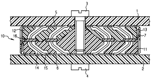
particularly, to Fig. 1 thereof, there is seen a printed circuit
board connector which represents a printed circuit board
--6-
CA 0219_7143 1997-03-04
GR 96 P 1039
connector according to an exemplary embodiment of the present
invention and is identified by reference numeral 10. In a
connection position shown in Fig. l, the printed circuit board
connector 10 is disposed (clamped) between first and second
parallel printed circuit boards 1 and 2, and it is held in this
position through the use of screws 3 and 4. The printed circuit
boards 1 and 2 are respectively shown as upper and lower printed
circuit boards in Fig. 1. A first contact strip element 5 is
provided between the printed circuit board connector 10 and the
first printed circuit board l, and a second contact strip element
6 is provided between the printed circuit board connector 10 and
the second printed circuit board 2.
.A housing of the printed circuit board connector 10 includes a
lower part 11 and two upper parts 12 and 13 seen in Fig. 1. The
housing, or the components forming the housing, are electrically
conductively constructed, or in other words a=re preferably made
~~f metal or a material that contains metal.
Conduits 14 are formed inside the housing of 'the printed circuit
hoard connector 10. The conduits have a curved course as shown
in Fig. 1. In the connection position shown :in Fig. l, the
conduits extend substantially continuously from a surface of the
:First printed circuit board I. to a surface of the second printed
c=ircuit board 2.
CA 02197143 1997-03-04
-~~~ a
GR 96 P 1039
An elongated contact element 15 is extended inside each conduit
14 and spaced apart from the conduit walls. The elongated
contact element 15 can electrically connect a contact spot
(surface contact) provided on the surface of the first printed
circuit board 1 to a contact spot (surface contact) provided on
the surface of the second printed circuit board 2. The contact
elements 15 are constructed to be elastically bendable, at least
on their ends.
As long as the printed circuit board connector is not in the
connection position shown in Fig. 1, outer ends of the contact
elements 15 protrude out of the conduits 19 at both sides of the
conduits. When the printed circuit board con:r~ector is moved into
the connection position shown in Fig. 1, end portions of the
contact elements 15 are pressed backward into the respective
conduits, in the process of the clamping of the printed circuit
board connector between the first and second electrical printed
~~ircuit boards. In the connection position of the printed
~~ircuit board connector, the end portions of the contact elements
exert a contact pressure force an the contact spots to be
~~ontacted on the surfaces of the printed circuii~ boards, and as a
.result they assure high contact forces, or in other words a
strong and reliable printed circuit board connection, from the
surface of one printed circuit board to another.
__g_
CA 02197143 1997-03-04
GR 96 P 1039
The electrical connection of the printed circuit boards solely
through surface contacts aids in reducing reflection from the
connection points and thereby enables a considerable lessening of
signal distortion, since there is no or at least no significant
overlap in the current flow direction of the elements that effect
the electrical connection. Moreover, it enables a simpler, more-
stable construction of the printed circuit boards in the
connection region (without any connection holes for press-fitting
an electrical connector into the printed circuit board).
In the connection position of the printed circuit board
connector, the contact elements 15 are substantially surrounded
entirely, over their entire length, by the walls of the conduits
14.
approximately in the middle between the ends of the conduits (at
a boundary between the lower part 11 and the upper parts 12 and
13 of the housing of the printed circuit board connector), each
~~f the contact elements 15 are retained by a :retaining element
L6. The retaining elements 16 are each solid:Ly connected to the
:respective contact elements 15. The retaining elements 16 have
dimensions that exceed the internal dimensions of the respective
conduits 14. They are inserted into suitable recesses between
i~he lower part 11 and the upper parts 12, 13 of the printed
--9-
CA 02197143 1997-03-04
GR 96 P 1039
circuit board connector housing, in such a way that in the
assembled state of the printed circuit board connector they are
immovably connected to the connector.
The retaining elements 16 (partly in cooperation with the contact
elements 15 retained by them) have multiple functions: First of
all, they are intended to prevent the contact elements 15 from
touching the electrically conductive conduit walls. Moreover,
they are intended to prevent the contact elements from being
displaceable along the various conduits. Finally, however, they
are also intended to enable a defined motion of the contact
elements inside the conduits (for instance, a motion parallel to
a conduit wall that defines the impedance, especially when the
printed circuit board connector is put into its connection
position) and to preclude other motions, for instance by a
suitable cross-sectional construction or the like, above all of
the contact elements.
The contact elements 15 are disposed substantially symmetrically
with respect to the retaining elements 16, at least in their
immediate vicinity, or are disposed in such a way that the forces
exerted on the retaining elements 16 by or through the contact
elements 15 have a substantially symmetrical course with respect
v~o the retaining elements, at least in their :immediate vicinity.
It is possible as a result for the forces exertE=_d on the
--10-
CA 02197143 1997-03-04
~9
GR 96 P 1039
retaining elements 16 by or through the contact elements 15 to
cancel one another out at least partially in the region of the
retaining elements 16. The retaining elements 16 themselves,
along with the printed circuit board connector housing, the
connection between the retaining elements and. the contact
elements, and in particular the anchoring of the retaining
elements in the printed circuit board connector housing, as a
result may have only a relatively slight stability and be
correspondingly small, without problems. The printed circuit
board connector according to the invention can therefore be
constructed to be relatively small and/or can have a very high
contact density (given a close-together configuration of the
contact elements or rows of contact elements, optionally with
internesting thereof).
'The contact strip elements 5, 6, as already noted above, are
provided between the printed circuit board connector and the
electrical printed circuit boards. These contact strip elements
;ire electrically conductively constructed and serve to make an
electrical connection between ground contacts of the printed
circuit boards to be connected to one another.
However, no separate contact elements 15 are provided in the
present exemplary embodiment for connecting the ground contacts.
wnstead, the electrical connection between the ground contacts of
--11-
CA 02197143 1997-03-04
GR 96 P 1039
the various electrical printed circuit boards is accomplished by
a different kind of establishment of a continuous electrical
connection path. The connection path namely extends from the
ground contacts of the first printed circuit board 1 through the
associated first (electrically conductive) contact strip element
5, the (electrically conductive) housing of the printed circuit
board connector, and the second (electrically conductive) contact
strip element 6, assigned to the second electrical printed
circuit board 2, to the ground contacts of the second electrical
printed circuit board 2.
This kind of ground connection has various kinds of advantages.
On one hand, the number of contact elements 15 to be provided in
the printed circuit board connector can be reduced quite
considerably under some circumstances as a result, and on the
ether hand, the grounding of the housing of the printed circuit
J~oard connector has the positive effect of ensuring that the
~~ontact elements 15, extending entirely inside the conduits 14,
~~re perfectly shielded from one another over ltheir entire length,
vhus reducing the danger of crosstalk or other mutual influences
i~o a minimum.
In order to enable an assurance of a perfect contact-making
between the ground contacts of the printers circuit boards and the
housing of the printed circuit board connector-, the contact strip
--12-
CA 02197143 1997-03-04
GR 96 P 1039
elements 5, 6 have resilient contact laminations at the top and
bottom. The contact strip elements have corresponding recesses
at those locations where contact spots of the printed circuit
boards are to be connected to the contact elements 15 of the
printed circuit board connector. However, many ground contacts
for which contact can be made by the contact strip elements may
be provided, particularly in the immediate vicinity of such
recesses, that is around the conduit openings.
Two of the possible embodiments of such contact strip elements
are shown in Figs. 2a a:nd 2b. In order to illustrate the mode of
operation of such contact strip elements, the contact strip
element shown in Fig. 2b is shown in Fig. 2c in a state in which
it is fastened between two surfaces to be electrically connected
to one another.
'The aforementioned contact strip elements 5, 6 are components of
a two-part mounting frame that is capable of :receiving the
printed circuit board connector inside it. More specifically,
vhe first contact strip element forms a top side of a half-shell-
>haped first half of the mounting frame, and the second contact
:trip element forms a bottom side of a half-shell-shaped second
half of the mounting frame. Each of the contact strip elements
moreover have extensions that form side elements of the halves of
the mounting frame but that no longer need to have a structure of
--13-
CA 02197143 1997-03-04
GR 96 P 1039
the kind shown in Figs. 2a and 2b and instead can be structured
arbitrarily differently.
Spring tabs 7 are provided on the side parts of the respective
halves of the mounting frame and can lock in detent fashion in
corresponding recesses in the housing of the printed circuit
board connector. As is shown in Fig. 1, the lower half of the
mounting frame, in terms of Fig. 1, can lock in detent fashion to
the top parts 12, 13 of the printed circuit board connector
housing, and the half of the mounting frame at the top in Fig. 1
can lock in detent fashion to the lower part 11 of the printed
circuit board connector housing.
The multi-part construction of the printed circuit board
connector housing, which is shown in Fig. l, serves to make it
simple to put the connector together: First, the contact
elements 15, with the retaining elements 16 secured to them, are
inserted into the lower part 11 of the printed circuit board
connector housing or more precisely into the conduit parts
provided in that portion. They are introduced .in such a way that
the retaining elements 16 come to rest in corresponding recesses
can the top of the lower part 11 of the printed circuit board
connector housing. Once all of the conduits :l4 have been
f~quipped with contact elements 15, the two upper parts 12, 13 of
1=he printed circuit board connector housing ar_e placed on the
--14-
CA 02197143 1997-03-04
GR 96 P 1039
lower part, with these elements initially merely resting loosely
on one another.
The placement of the upper parts on the lower part is carried out
by an obliquely extending placement motion. More specifically,
the upper part 12 on the left in the drawing is put in place
through the use of a movement from the upper right to the lower
left, and the upper part 13 on the right in the drawing is put in
place through the use of a movement from the top left to the
bottom right. The extent of the oblique motion depends on the
shape of the contact elements. In the ideal case, slipping the
upper parts over the upper half of the contact elements, that is
the upper half in terms of the drawing, is carried out in such a
way that the contact elements do not touch the conduit walls at
all, or at most only slightly, or in other words are
substantially parallel to the course of the contact elements in
the region to be covered. In this way, damage to the conduit
walls and/or the contact elements during mounting can be
maximally avoided. Another favorable factor :is that not only all
of the contact elements onto which the upper :Left part 12 in the
drawing is placed but also all of the contact elements onto which
~~he upper right part 13 in the drawing is placed, extend parallel
to one another. The contact elements belonging to different
groups (to be covered by different upper part;>) are not
constructed in the present exemplary embodiment as parallel but
--15-
"~1 .,.,. . .. . .
CA 02197143 1997-03-04
"~, ,
GR 96 P 1039
rather symmetrical to one another, for the sake of attaining a
symmetrical distribution of force with respect to the connection
of the electrical connector to the printed circuit board to be
connected, as will be described below.
In order to make quite certain of the aforementioned oblique
placement motion, the lower part has a protrusion of the kind
shown in the drawing, with two inclines facing one another, along
which the upper parts can be guided (can slide downward) as they
are placed on the lower part. The inclines that are clearly
visible in the drawing have a course which is essentially
parallel to the course of the contact element portions that are
each to be covered by the associated upper parts. However, the
inclines need not extend straight as shown in the drawing, but
instead (preferably with close reliance on the shape of the
contact elements) may a.Lso have any arbitrary other shape (for
instance being stairstep-like or curved).
In order to attain an even more precisely defined guidance of the
pper parts on the guided inclines of the lower part, and
therefore an even more-perfect guidance of the contact elements
inside the conduits when the upper parts are placed on the lower
part, or more specifically to also prevent a :Lateral offset of
the upper parts and lower parts when they are placed one another
the other, the guide inclines may be provided with guide
--16-
. .~.", . ,.v .. . .. ".., ._ ,. .. ,.,. ..
CA 02197143 1997-03-04
GR 96 P 1039
elements, for instance in the form of rails or grooves, that
extend straight or obliquely or curved on their surface, and
which can be engaged by suitable complementary elements of the
upper parts.
The above-described embodiment of the components of a multiple-
part electrical connector can be usefully employed not only in
the type of printed circuit board connector described herein but
also quite generally in any kind of electrical connector. Such
an embodiment reliably makes it possible to put together
connector components simply and without force while at the same
time securing the contact elements of the electrical connector.
The upper parts and lower part are held together through the use
of the detent locking o:E the configuration having the mounting
frame halves, already was explained above.
In the state in which engagement with the mounting frame has been
brought about, the printed circuit board connector is prepared
for making a connection with printed circuit boards that are to
be connected to one another.
'The connection is made by fasteners, such as i~he screws 3, 4, of
which a plurality are disposed in line with one another in the
~.1. ~ . ".,. . . . .. .. .."a. ~ . ._..~.. ,~.. . ~ . . .
CA 02197143 1997-03-04
_~ _:
GR 96 P 1039
view of Fig. 1 and which enter alternatingly from above and from
below.
The alternating fastening of opposed sides of the configuration
makes it possible to provide a high density of fasteners, which
in turn makes it possible for even small printed circuit board
connectors to be reliably firmly connected to the printed circuit
boards that are to be connected to one another.
The connection of the elements by screws can :be achieved in the
:host various ways (screwing into the printed circuit board
connector housing, screwing with nuts, screwing a. plurality of
screw elements in one another in internested fashion, and so
forth).
regardless of the type of fastener, it proves to be advantageous
:if the printed circuit board connector is clamped as uniformly
:strongly as possible between the printed circuit boards to be
:joined together, with the additional interposition of the contact
;trip elements, because in this way on one hand uniformly good
connections are obtained, and on the other hand the resultant
distribution of force to the contact elements leads to an
improved force compensation in the region of t=he retaining
elements 16.
__1g_
~~.. " ,...M"... .,.. ....~.w. .z..~.
CA 02197143 1997-03-04
GR 96 P 1039
It may also be worthwhile to construct or select the printed
circuit board connector and the fastener, or to define the use of
these elements, in such a way that the connection between the
printed circuit board connector and the first printed circuit
board and the connection between the printed circuit board
connector and the second printed circuit board, are made
simultaneously and each to the identical extent. As a result,
the aforementioned force compensation can already be realized as
the printed circuit board connector is introduced into its
connecting position as well as when the printed circuit board
connector is released from this position.
The present description has related to a printed circuit board
connector for transmitting asymmetrical signals (one internal
~~onductor and one common outer conductor each). The printed
circuit board connector described herein, optionally with
suitable modification, can also be used for transmitting
;symmetrical signals (two internal conductors).
In the case where asymmetrical signals are transmitted, that is,
if only one internal conductor is provided, an .impedance of the
sprinted circuit board connector is settable by setting (and
maintaining) a spacing between the internal conductor and an
:impedance-determining side wall of the conduit.
--19-
CA 02197143 1997-03-04
GR 96 P 1039
In the event that symmetrical signals are transmitted, that is,
if two internal conductors are provided, an impedance of the
printed circuit board connector can be adjusted by setting (and
maintaining) a spacing between the two (internal) conductors and
by setting a spacing between the two internal conductors and an
impedance-determining side wall of the conduit.
In order to ensure that an impedance value once set will be kept
constant under all circumstances, the conduits 14, contact
elements 15 and retaining elements 16 should be constructed in
such a way that the elastic motion of the contact elements 15
inside the conduits 14 that takes place when the printed circuit
board connector is introduced into and/or released from its
connecting position, is possible solely in directions which do
not cause any change in impedance (an example being a motion
parallel to an impedance- determining wall).
--20-