Note: Descriptions are shown in the official language in which they were submitted.
~wo 96/09687 2 ~ ~ ~ 3 2 ~ PCT/US9S/12145
ElIGEI EFFICIENCY VOLTAGE CONVERTER AND REGULATOR
CIRCUIT
Field of the Invention
The present invention generally relates to apparatus and a method for
5 converting an alternating current (AC) to a direct current (DC), and more
specifically, to apparatus and a method for rectifying the AC to produce a rectified
signal and regulating the rectified signal to limit the voltage of the DC supplied to
the load.
p.~r.kPround ofthe JnvenfiQn
A component required in almost all non-battery powered electrical devices
that require DC is a power supply that will couple to an AC line and convert theAC to DC. There are many designs in the prior art for power supplies to
accomplish this function. Most AC-DC switching power supplies that are directly
powered by the AC line employ a l~ 'u~ to isolate the line side of the circuit
1~ from the output side. A winding on the il~l,rullll in such circuits is sometimes
employed to provide an AC voltage that is rectified to DC and used to provide
power to a control circuit on the line side of the power supply. The ~ ,ru~
and associated CU~ J ~ used for this purpose are referred to in the followmg
discussion as an AC-DC voltage converter.
For certain _,, ' , it is desirable that the power supply or AC-DC
converter comprise as few ~ as possible to minimize its cost. In some
low cost AC-DC voltage converter designs, a resistor having a high power rating is
used to reduce the line voltage instead of a I~ rull~l~,., and the DC voltage level is
regulated using a zener diode. The current limiting resistor that is used for this
25 purpose tends to dissipate ,,1,.1,1~. energy as heat, due to the I2R losses in the
resistor. Because of the power losses in the resistor, this type of converter is very
inefricient. For ;.,I r~ ~1 use in countries where the AC voltage levels are much
higher than in the U.S., this type of simple design may be unusable because the
21~73~
wo 96/09687 . ~ ,,~ L~145
heat generated in the resistor causes its L~ dLul~ to rise to an ~ aAI.I.
Ievel. Thus, an alternative design for a low cost, low part count power
7uyyl~,u..~,. Ia is required that lS efficient and can operate over a wide range of
line voltage levels, including those used in other co~mtries. Such a converter can
5 be used alone as an inexpensive power supply, where precise regulation, isolation,
and low ripple on the DC output are not crrtical, or as the source of tbe power
required by the line side control circuit of a switching power supply.
Sllmm ~y of the Inveniûrl .
In accordance with the present invention, a voltage converter for
10 converting an AC line signal to a DC output signal supplied to a load is defined.
The voltage converter includes a full wave rectifier that converts the AC line signal
to a full wave rectified sigmal comprising a plurality of aulJaLd~Lially identical
successive half cycle waveforms. A capacitor adapted to be coupled in parallel
with the load is also provided. First switching means, coupled to the fiull wave15 rectifier and to the capacitor, conduct a charge current to the capacitor at least
once during each half cycle waveform. Second switching means, coupled to the
full wave rectifier, the capacitor, and the first switching means, are operative to
regulate a ~ of the first switching means as a function of both the DC
output signal and the fiull wave rectified signal, both of which vary with time. The
20 second switching means thereby regulate the DC output signal by controlling the
current applied to charge the capacitor so that the voltage across the capacitordoes not exceed a yl rd~ . ~I maximum level
In one r",l.o,l;.l...,l the second switching means comprise one transistor
and a zener diode. In another clllbo~l;n~ the second switching means comprise a
25 zener diode, and a pair of transistors, each having a base, an emitter, and acollector. The pair of transistors have their collectors coupled together and their
emitters coupled together, to form a differential pair. The first switching means
preferably comprise a metal-oxide 7 ~ field effect transistor (MOSFET)
having a gate coupled to the second switching means so that the second switching30 means control the voltage applied to the gate and thus control the conductive state
of the MOSFET.
The voltage converter further comprises a carbon resistor coupled in series
between the full wave rectifier and the first switching means. If current flow
through the carbon resistor ~ub~l~lLidlly exceeds a maximum rated value as a result
35 of a fault in one of the first switching means and the second switching means, the
carbon resislor fails in an open circuit mode, hlL~IIUIJLilll7 the current flow to said
21~322
0 96/09687 . ~ 12145
one of the first and the second switching means and to any load coupled thereto.To provide further protection in one r~ o l; ,. , a zener diode is preferably
coupled in parallel with the second switching means. The zener diode limits a
voltage applied to the load if a fault occurs in the second switching means.
A further aspect of the present invention is a method for converting an AC
signal to a DC signal. The steps of the method are generally consistent with thefunctions of each of the elements of the voltage converter discussed above.
Brief Descrigtiorl of ~h~ Drawhlp Fi,~ures
The foregoing aspects and many of the attendant advantages of this
invention will become more readily appreciated as the same becomes better
understood by reference to the following detailed description, when taken in
" with the _ . ,;ng drawings, wherein:
FIGURE I is an electrical schematic diagram of a first ~ . ll,o~l;, .. .,l of a
voltage converter in accordance with the present invention;
FIGURE 2A is graph showing the relationship between a full wave rectified
signal and a reference voltage in the first rl 111 lo~1 ~f of the voltage converter;
FIGURE 2B is a graph showing current pulses that charge a capacitor in
the first ,,..I,.,,I;,.,...-,
FIGURE 2C is a graph showing the ripple on the DC output voltage of the
20 firstr",l,o.l;"' ofthevoltageconverter;
FIGURE 3 is an electrical schematic diagram of a second preferred
I,od;ll~ L of the voltage converter;
FIGURE 4A is a graph showing a full wave rectified signal developed in
the second ~
FIGURB 4B is a graph showing the current pulses that charge a capacitor
in the second c~llI")d;..l.,llL of FIGURE 3; and
FIGUR~ 4C is a graph showing the ripple on the DC output voltage of the
second ~lllI,od;lil~,llL of the voltage converter.
Description of the Preferred 1~" .1 " .. 8 ., ... ,~
As noted above, one of the objects of the present invention was to achieve
conversion of AC to DC using a circuit having relatively few cw.ll.~ , which is
both . ~ and efficient. A high efficiency voltage converter 10, which
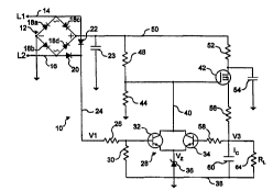
achieves this object, is shown in a schematic diagram in FIGURE 1. W-lth
reference to FIGURE 1, AC line voltage is coupled to voltage converter 10 on
lines ]4 and 16. Although the voltage level of the AC supplied to the voltage
converter in the U.S. is typically in the range of 110 to 120volts, and the
w0 96/09687 2 1 9 7 3 ~ 45 --
frequency of the AC is 60 Hz, voltage converter 10 can operate equaUy weU if
supplied with other AC frequencies and line voltages on lines 14 and 16, for
example, 50 Hz at 220 volts AC, as is common in many foreign countries.
Voltage converter 10 includes a full wave rectifier bridge module 12 that
S internally comprises four diodes 18a-18d. Four discrete diode connected m a fuU
wave rectifier bridge can also be used for this purpose As shown on the Figure,
the cathodes of &odes 18a and 18b are lta~ coupled to lines 14 and 16,
and their anodes are grounded. Similarly, the anodes of diodes 18c and 18d are
coupled to lines 14 and 16, and their cathodes are coMected to a
10 line 50. A full wave rectified signal from the bridge is thus applied to line 50,
referenced to ground.
Line 14 is also connected to the anode of a diode22, and line 16 is
coMected to the anode of a diode 20. The cathodes of diodes 20 and 22 are
coMected together to a line 24 to provide a second full wave rectified signal Vl,
15 as shown in FIGURE 2A
Referring again to FIGURE 1, the full wave rectified signal Vl on line 24 is
input through a resistor 26 to the base of a transistor 32. The base of transistor 32
(NPN) is also coupled to ground through a resistor30. Transistor32 and a
transistor 34 (NPN) comprise a differential pair 28, because their collectors are
20 connected together to a line40 and their emitters coMected together to the
cathode of a zener diode 36. The anode of zener diode 36 is grounded through a
line 38. The base of transistor 34 is coupled to receive the voltage applied to a
load 64 having a resistance RL. In addition, a capacitor 60 is coMected in parallel
with the load, one side of capacitor 60 bein~ connected to resistor 58 and the other
25 side being connected through line38 to ground. The load is also coupled to
ground through line 38.
The full wave rectified signal output from full wave rectifier 12 is at least
partially filtered by a capacitor 23 that is connected between iine 50 and ground. A
resulting filtered signal on line 50 is applied through a resistor 52 to the drain of an
30 N ' l, metal-oxide s~ field effecttransistor (MOSFET)42. The
gate of MOSFET 42 is also coupled to line 50 through a resistor 48, and to ground
through a resistor 44. Resistors 48 and 44 comprise a voltage divider to reduce
the filtered signal on line 50 to a level suitable for input to the gate of the
MOSFET. The gate of MOSFET42 is also coMected to the collectors of
transistors 32 and 34 through line 40. As explained below, both of these
transistors control MOSFET 42. A resistor 56 couples the source of MOSFET 42
~wo 96/09687 2 1 9 7 3 2 ~ 2~4s
to the common node at which resistor 58, capacitor 60, and load 64 are connected,
and a capacitor 54, which is connected between the drain and ground, provides
additional filtering
Load 64 is supplied DC from capacitor 60, drawing its voltage level down
5 as it discharges the capacitor. Capacitor 60 is p.,.;odh,OI y recharged by current
flowing through the drain and source of MOSFET 42. However, this charge
current, Ic, only flows through MOSFET 42 when its gate is biased to a voltage
more positive than its source. The voltage applied to the gate of MOSFET 42
varies with the voltage level of the filtered signal on line 50, subject to the
conductive state of transistors 32 and 34. Transistor 34 and MOSFET 42 together
serve as a voltage regulator that regulates the voltage on capacitor 60 and thus,
across load 64. Transistor 32 controls the portion of each half cycle during which
this voltage regulator is enabled.
When it is fully saturated and in a conductive state, transistor 32 couples
15 line 40, which is connected to the gate of MOSFET 42, to the cathode of zenerdiode 36. The conductive state oftransistor 32 is controlled by the voltage applied
to its base through resistor 26. That voltage, which is a full wave rectified signal
having a waveform 70 as shown in FIGllRE 2A, p~,.;udh,~lly varies between zero
and some nominal value deterrnined by the resistance ratio of resistors 26 and 30.
20 In order for transistor 32 to conduct between its collector and emitter, the base of
transistor 32 must be biased to a level more positive than a ~ zener
voltage, Vz, of zener diode 36. For example, if the zener voltage of zener diode 36
is 12.6 volts, transistor 32 will become fully saturated in a conducting state when
waveform 70 is substantially greater than the sum of the nominal zener voltage Vz
25 and the basc CA. ~ voltage drop (about 0.6 volts).
For purposes of the following discussion, the base-emitter voltage drop of
transistors 32 and 34 is ignored, so that the reference level is simply the zener
voltage Vz, as shown by the dash line in FIGURE 2A. As soon as the voltage
input to the base of transistor 32 falls below the zener voltage Vz, transistor 32
30 turns off, i.e., conduction between its collector and emitter ceases. While
transistor32 is in a conductive state, the gate of MOSFET42 is effectively
clamped at the zener voltage level. As the voltage applied to the base of
transistor 32 drops below Vz, causing transistor 32 to stop conducting,
MOSFET 42 begins conducting current Ic from the filtered signal on line 50 in
35 order to charge capacitor60. Current Ic continues to flow into capacitor60
through MOSFET 42 until either transistor 32 or transistor 34 turns on.
wo g6/09687 2 1 ~ ~f3 2 2 F~ 4~--
Transistor34 also controls ' of charge current Ic through
MOSFET42. The base of transistor34 is coupled through resistor58 to
CapACitOr 60, to sense the voltage across the capacitor and load 64. If the voltage
applied to the base of transistor 34 is aubaio~ '!y greater than the zener voltage of
zener diode 36, transistor 34 is biased into a saturated condition and conducts
between its collector and emitter terminals, thereby effectively comnecting the gate
of MOSFET 42 to the cathode of zener diode 36. Just as explained above in
connection with transistor 32, conduction through transistor 34 turns off
MOSFET 42 so that charge current Ic no longer flows into capacitor 60 (and to
10 the load). It will therefore be apparent that transistor 34 controls the MOSFET as
a function of the voltage level across capacitor 60, ensuring that the voltage never
exceeds the zener voltage Vz. Accordingly, charge current Ic comprises a series of
pulses 72 as shown in FIGVRE 2B, each lasting for some time intenal toD, which
varies depending upon RL, and thus the rate at which the load dLscharges
15 capacitor 60. The time intenal toD starts when two conditions occur. First, the
voltage applied to the base of transistor 32 must be less than the zener voltage, as a
function of amplitude of the full wave rectif ed signal applied to its base. Second,
the voltage on capacitor 60 and across the load must be less than the zener voltage.
As current flows through MOSFET 42 to charge capacitor 60, the voltage across
20 the capacitor rises until it is al~,u~ WLlllldt.,l,~ equal to the zener voltage, V2, CaUSLng
transistor 34 to turn on, or until the voltage input to the base of transistor 32 again
p~i ~ rises above the zener voltage, whichever condition occurs first. When
current flow through MOSFET 42 ceases, the voltage level across capacitor 60
declines as current is drawn through the load, with a rate of discharge, I, which is
25 equal to the product of the resistance, Ra of the load 64 and the t~Dp~eit~n~, C, of
capacitor 60. The ripple component of the voltage across the load is shown in
FIGURE 2C, as a waveform ?2. It should be noted that the vertical scale is
'l~, expanded in this Figure; the ripple voltage range is typically less than
ten percent of the DC output voltage level.
A high efficiency voltage converter 100, comprising a second allll,.,.i;.,.. 1
of the present invention, is shown in FIGURE 3. Where appropriate, the same
reference numerals are used for ~ of voltage converter 100 as were used
for voltage converter 10. Thus, for example, the AC line voltage input to the
voltage converter is conveyed on lines 14 and 16. Similarly, the DC output signal
3~ supplied to load64 is provided from the charge on capacitor60. However,
different reference numerals are used for other ~--~l of voltage
~W 2~97~22j
0 96/09687 . r- r~ 14s
converter 100, even where they provide a sinnilar function to the ~ l of
voltage converter 10, if that function is at all different than explained above.The AC signal input on lines 14 and 16 is again full wave rectified. In
voltage converter 100, four discrete diodes 102-108 are employed to full wave
5 rectify the AC hne voltage. In this ,, t, the anode of diode 102 and the
cathode of diode 108 are connected to hne 14. Similarly, the anode of diode 104
and the cathode of diode 106 are connected to line 16. The cathodes of
diodes 102 and 104 are jointly connected to a resistor 110, and the anodes of
diodes 106 and 108 are coupled to ground through a line 130.
The opposite side of resistor 110 is connected tbrough a line 112 to a
resistorll4,aresistorll6,andtothedrainofaMOSFET118. Theothersideof
resistor 114 is connected tbrough a line 120 to the gate of MOSFET 118 and to
the collector of a transisto} 122 (NPN). Line 120 is also connected to the cathode
of a zener diode 134.
The base of transistor 122 is coupled to the full wave rectified signal on
line 112 (again identified as Vl) as shown by a waveform 140 in FIGURE 4A,
tbrough resistor 116. Resistor 116 is connected to the base of the transistor
through a line 124, which also connects to the load tbrough a resistor 126 and ahne 128. Line 128 couples the load to capacitor 60 and to the source of
MOSFET 118.
A zener diode 132 is connected to the emitter of transistor 122 and its
~,Lrlh~,h,li~Lic zener voltage Vz again determines the maxirnum voltage apphed to
the load and to charge capacitor 60. The anode of zener diode 132 is coupled to
ground through line 130.
Charge current Ic supplied to capacitor 60 (and to the load) 'dows through
MOSFET 118 between its drain and source ter ninals, when the MOSFET is in a
conducting state. The f.,l,.l,.. Ihll. ~ of MOSFET 118 is controlled by the voltage
applied to its gate tbrough line 120. The voltage on line 120 in turn depends upon
full wave rectified voltage Vl and the conductive state of transistor 122. Whiletransistor 122 is not conducting, the voltage on line 120 has a waveform similar to
that shown in FIGURE 4A. However, when transistor 122 begins conducting
between its collector and ernitter as it becomes saturated, the voltage on line 120 is
effectively clamped at the zener voltage, .1 - h .I rl ;~1 ;r. level of zener diode 132.
Transistor 122 becomes saturated when its base is biased to a level
~ub~LhllL~ y more positive than the zener voltage of zener diode 132. The voltage
applied to the base of transistor 122 is a function of the voltage across capacitor 60
wo 96/09687 219 7 3 2~,2 PCT/US95/12145 ~!
(and the load), conveyed through resistor 126, and is also a function of the full
wave rectified voltage on line 112, which is conveyed through resistor 116. Whenthe full wave rectified voltage applied to the base of transistor 122 through
resistor 116 is more positive than the zener voltage of zener diode 132,
transistor 122 becomes saturated and conducts, turning off MOSFET 118 by
coupling its gate to zener voltage level. Resistor 116 has a ~ greater
resistance than resistor 126, but its connection to the full wave rectified voltage
causes it to exercise primary control of Lu~Ju~,LiYiLy tbrough transistor 122, and of
MOSFET 118.
The zener voltage of zener diode 132 thus determines the maximum
voltage developed across capacitor 60 and load 64. Because the voltage across
capacitor 60 is cullfi~ vu~ly being drawn down by the discharge current flowing
through load 64, but is only '~, recharged by current flowing through
MOSFET 118, there is a significant ripple component in the voltage applied to the
load. The ripple voltage on the DC output signal is shown as a waveform 146 im
FIGURE 4C. Voltage converter 100 has slightly less ripple than voltage
converter 10, because voltage converter 10 charges the capacitor that supplies
current to the load for a shorter total time during each half cycle. As current flows
from capacitor 60 through the load, capacitor 60 discharges and its voltages drops
below its peak value, Vz. The voltage ~ub~cuu~,llLly increases in steps, as
successive pulses of current are applied to charge capacitor 60 through
MOSFET 118, as explained below. The rate of discharge of capacitor 60, ~, is
equal to the product of the r~p~ ~it~r~e~ C, of capacitor 60 and the resistance of the
load, RL. Because the ripple voltage is shown on an expanded scale in
FIGURE 4C, it may appear to be excessive; however, the ripple voltage range is
typically less than ten percent of the DC output voltage level.
In FIGllRE 4B, the pulses of current Ic applied to charge capacitor 60 are
shown. During each half cycle of the full wave rectified signal Vl, two current
pulses are applied through MOSFET118. As the full wave rectified signal
represented by waveform 140 in FIGURE 4A decreases from its peak to ~ro, the
voltage on the base of transistor 122 drops below the zener voltage Vz, and
transistor 122 stops conducting. The voltage applied to the gate of MOSFET 118
through resistor 114 then causes MOSFET 118 to begin conducting between its
drain and source, thereby charging capacitor 60 with a pulse of current 142, as
shown in FIGI~RE 4B.
21g7322
~wo 96/~9687 ~ P~ 4~
.sly~ current pulse 142 ends as the voltage across capacitor60
rises sufficiently to turn on transistor 122. The voltage across the capacitor, which
is applied to the base of transistor 122 through resistor 126, biases the transistor to
a conducting state, which reduces the voltage on the gate of MOSFET 118 below
the level necessa~y for it to continue conducting. Alternatively, if the voltageacross capacitor 60 (and load 64) does not reach a level sufficient to turn on
transistor 122, the full wave rectified voltage level on line 120 will decline to a
level that is insufficient to continue biasing MOSFET 118 into a conductive state.
A second current pulse 144 is produced as the full wave rectified waveform
voltage begins increasing from zero towards its peak value during the next half
cycle. This voltage again causes MOSFET 118 to conduct charge current Ic to
capacitor 60. As the full wave rectified signal applied to the base of transistor 122
through resistor 116 rises above the zener voltage, Vz, the transistor turns on,turning offMOSFET 118 and ending the current pulse. So long as the voltage
applied to the base oftransistor 122 through resistor 126 or through resistor 116
does not ' "y exceed the zener diode ~ ; 0, zener voltageVz,
transistor 122 will remain in a non-conducting state. Accordingly, the charge
current for the second Ic pulse applied to capacitor 60 terminates when the voltage
applied to the base of resistor 122, either from capacitor 60 through resistor 126 or
from line 112 through resistor 116 exceeds the zener voltage.
By providing two pulses of current to charge capacitor 60 each half cycle,
voltage converter 100 is more effective than voltage converter 10 in minimizing
ripple in the voltage across the load. F~ll L~ lul ~, since charge current is supplied
to capacitor 60 and to the load for a long duration during each half cycle, voltage
converter 100 operates more efficiently than voltage converter 10.
If a fault occurs, voltage converters 10 and 100 can apply full line voltage
across the load. To protect against tbis possibility, the MOSFETs used in the
voltage converters are selected to have a ~ peak drain-to-source
voltage rating that is ~uh~L~lL '~ greater than the expected peak line voltage. In
addition, the voltage converters each include an inherent fuse to protect the load if
a fault occurs. Resistor52 m voltage converter 10 and resistor 110 in voltage
converter lû0 are .,u~ carbon resistors, which almost always fail in an
open circuit mode if subjected to power dissipation ~..b~L~lL "y in excess of the
maximum rated value. ln voltage converter 10, resistor 26 is also a carbon
35 resistor. If these carbon resistors open due to excess current flow through them,
any line voltage across the load will be terminated. These resistors thus act much
wo 96/09687 2 ~ 9 7 3 ~ 2 ~ J/i2l4s
like fuses to protect against short circuit conditions in the MOSFETs and other
AddGtional fault protection is provided in voltage converter 100 by zener
dGode 134. This zener diode has a ..1.~ zener voltage selected to ensure
that failure of transistor 122 does not leave MOSFET 118 im a conductive state.
Although the present invention has been described in comnection with the
preferred t I '' ' disclosed above, it will be understood by those of ordinary
skill in tne art that many . .1;1~ can be made thereto witbin the scope of the
claims that follow. Accordingly, it is not intended that the scope of the invention
in any way be Gmited by the above description, but that it be determined entirely by
reference to the claims that follow.