Note: Descriptions are shown in the official language in which they were submitted.
CA 02197491 2001-04-30
1
A Ferroelectric Capacitor and
a Method far Manufacturing Thereof
Field of the Invention
The present invention relates to a ferroelectric
capacitor and, more specifically, to improvement of the
ferroelectricity and ot;r.er characteristics of the capacitor.
Background art
Fig. 10 shows a conventional ferroelectric
capacitor. A silicon o~:idation layer 4 is formed on a
silicon substrate 2. A lower electrode 6 made of platinum
is provided thereon. A PZT (PbZr~ Til_~_ Oj) film 8 as a
ferroelectric layer is formed on the lower electrode 6, and
an upper electrode 10 made of platinum is provided thereon.
Thus, the ferroelectric capacitor is formed by the lower
electrode 6, the PZT fi1_m 8 and the upper electrode 10.
The reason to u~;Ee platinum for the lower electrode 6
is as follows. The PZT i=ilm 8 must be formed on a layer
which can be oriented, because the ferroelectricity of PZT
is degraded when the PZ'7, film is formed on a layer made of
amorphous material, since the PZT film cannot be oriented.
Meanwhile, the lower electrode 6 must be insulated from the
silicon substrate 2, therefore, the silicon oxidation layer
4 is formed on the silicon substrate 2. The silicon
oxidation layer 4 is amorphous. In general, although a
layer formed on an amorphous material becomes nonorientable,
a layer made of platinum has a characteristic of becoming
orientable even when it is formed on the amorphous matex-ial.
Therefore, platinum is used for forming the lower electrode
because of the reason dc~;~cribed above.
However, the con~rentional ferroelectric capacitor
has the following problf~m to be resolved.
The problem is degradation of ferroelectricity
3~~ caused by frequent rove=rsion of polarization, aging and
leakage of oxygen from t:he ferroelectric substance (PZT),
CA 02197491 2001-04-30
2
since platinum has a tendency of allowing oxygen and Pb to
pass through it. In other words, there is high probability
of leakage of oxygen and Pb contained in the ferroelectric
substance between the cclumnar crystals of platinum, as
shown in Fig. 11. The ~:roblem also arises in a capacitor
using a dielectric substance having high dielectric
constant.
Disclosure of the present invention
It is an object of the present invention to provide
a ferroelectric capacitor having less degradation of
ferroelectricity caused by frequent inversion of
polarization and aging or. a dielectric capacitor maintaining
high dielectric constant., both of which resolve the problem
described in the above.
The word "capacitor" in the present invention
defines structure havinct electrodes on both sides of an
insulator, also it is a concept having the structure stated
in the above regardless of whether it is used for electric
storage.
In accordance wi.t:h a first embodiment of the
invention, a ferroelect~~_Lc capacitor comprises:
a lower e.lectrocle having an oxidation layer
including at least one 7_ayer selected from a WOx layer, a
TiOx layer, a TaOx layer, an IrO, layer, a PtO, layer, an
RuOx layer, an ReOx layer, a PdOx layer and an OsOx layer,
a dielectric lager comprising either a ferroelectric
substance or a dielectric substance having a high dielectric
constant, the dielectric layer being formed on the lower.
electrode, and
an upper electrode formed on the dielectric layer.
By providing the lower electrode with at least one
oxidation layer selected from a WOx layer, a TiOx layer, a
TaOx layer, an Ir02 layer, a Pt0-. Layer, an RuOx layer, an
ReOx layer, a PdOx layer and an OsOx layer, it is possible
to prevent leakage of o:~ygen from the dielectric layer <~s
CA 02197491 2001-04-30
3
well as suppressing degradation of ferroelectricity by
aging.
Preferably, the lower electrode comprises a
conductive layer which includes at least one layer selected
from a W layer, a Ti layer, a Ta layer, an Ir layer, a Pt
layer, an Ru layer, an ~.e layer, a Pd layer and an Os layer
on the oxidation layer, and a ferroelectric layer is formed
on the conductive layer.
15
More preferably, the lower electrode is formed on a
silicon oxidation layer located on a substrate, and the
lower electrode has a cc>ntact layer in contact with the
silicon oxidation layer.
By providing the lower electrode with a conductive
layer which includes at. least one layer selected from a W
layer, a Ti layer, a T<~ ,'~ayer, an Ir layer, a Pt layer, an
Ru layer, an Re layer, a Pd layer and an Os layer on the
oxidation layer and providing a ferroelectric layer on the
conductive layer, leakage current can be decreased.
In accordance wi.t;h a second embodiment of the
invention, a ferroelectric capacitor comprises:
a lower electrode,
a dielectric lager comprising either a ferroelectric
substance or a dielect:r:_c substance having a high dielectric
constant, the dielectric: layer being formed on the lower-
electrode, and
an upper electrode formed on the dielectric layer
and including at least one layer selected from a WOx layer,
a TiOx layer, a TaOx la;rer, an IrO,, layer, a PtO~ layer, an
RuOx layer, an ReOx layer, a PdOx layer and an OsOx laye r.
By providing the upper electrode with at least one
oxidation layer selected from a WOx layer, a TiOx layer,. a
TaOx layer, an IrO~ layer, a Pt0= layer, an RuOx layer, an
CA 02197491 2001-04-30
4
ReOx layer, a PdOx layer and an OsOx layer, it is possible
to prevent leakage of oxygen from the dielectric layer as
well as suppressing degradation of ferroelectricity by
aging.
Preferably, the lower electrode is formed on a
silicon oxidation layer located on a substrate, and the
lower electrode has a contact layer in contact with the
silicon oxidation layer.
In accordance with a third embodiment of the
invention, a ferroelectric capacitor comprises:
a lower e:Lectrode having an oxidation layer
including at least one 1_ayer selected from a WOx layer, a
TiOx layer, a TaOx layer,. an IrO, layer, a PtO> layer, an
RuOx layer, an ReOx layer, a PdOx layer and an OsOx layer,
a dielectric la~~er comprising either a ferroelect:ric
substance or a dielectric substance having a high dielectric
constant, the dielectric: layer being formed on the lower
electrode, and
an upper electrode having an oxidation layer
including at least one 7_ayer selected from a WOx layer, a
TiOx layer, a TaOx layer, an IrO, layer, a PtOlayer, an
RuOx layer, an ReOx layer, a PdOx layer and an OsOx layer.
By providing both the upper and the lower electrode
with at least one oxidation layer selected from a WOx layer,
a TiOx layer, a TaOx lays=_r, an IrO, layer, a PtO~ layer, an
RuOx layer, an ReOx layer, a PdOx layer and an OsOx layer,
it is possible to prevemr_ leakage of oxygen from the
dielectric layer as wel=L as suppressing degradation of
ferroelectricity by aging.
Preferably, the lower electrode comprises a
3~ conductive layer which :includes at least one layer seler_ted
from a W layer, a Ti las~~~r, a Ta layer, an Ir layer, a I?t
layer, an Ru layer, an Re layer, a Pd layer and an Os layer
CA 02197491 2001-04-30
on the oxidation layer, and a ferroelectric layer is formed
on the conductive layer-.
More preferably, the lower electrode is formed on a
5 silicon oxidation layer Located on a substrate, and the
lower electrode has a cc>ntact layer in contact with the
silicon oxidation layer.
By providing at least one layer selected from a W
layer, a Ti layer, a Ta 7_ayer, an Ir layer, a Pt layer, an
Ru layer, an Re layer, ~~ Pd layer and an Os layer on the
oxidation layer and providing a dielectric layer on the
conductive layer, leakage current can be decreased.
Thus, in accordance with the invention, a
ferroelectric capacitor which offers excellent
ferroelectricity and h:ic~h dielectric property is attainable.
In accordance wi.t;h a further aspect of the
invention, a method of manufacturing a ferroelectric
capacitor comprises the :steps of:
forming at least: one oxidation layer selected from a
WOx layer, a TiOx layer, a TaOx layer, an IrO~ layer, a Pt~O
layer, an RuOx layer, an ReOx layer, a PdOx layer and an
OsOx layer on a substrat;f=_ as a lower electrode by
sputtering,
forming either ~i ferroelectric film or a dielectric
layer having a high die=Lc=ctric constant on the lower
electrode as a dielectr_Lc layer, and
forming an upper electrode on the dielectric layer.
In accordance wit=h a second method embodiment of: the
invention, a method of manufacturing a ferroelectric
capacitor comprises the ;steps of:
3~ forming at least: one layer selected from a W layer,
a Ti layer, a Ta layer, an Ir layer, a Pt layer, an Ru
layer, an Re layer, a Pd layer and. an Os layer on a
CA 02197491 2001-04-30
6
substrate as a base layer by sputtering,
oxidizing a surface of the base layer,
forming either a ferroelectric film or a dielectric
layer having a high dielectric constant on the base layer as
a dielectric layer, a surface of the base layer being
oxidized, and
forming an upper electrode on the dielectric layer.
In accordance with a third method embodiment of the
invention, a method of manufacturing a ferroelectric
capacitor comprises the :steps of:
forming either a. ferroelectric film or a dielectric
layer having a high dielectric constant on a lower electrode
as a dielectric layer, dTld
forming at least. one oxidation layer selected from a
WOx layer, a TiOx layer, a TaOx layer, an IrO~ layer, a Pt=O
layer, an RuOx layer, an ReOx layer, a PdOx layer and an
OsOx layer on the dielectric layer as an upper electrode by
sputtering.
In accordance wi.t:h a fourth method embodiment of the
invention, a method of r:ranufacturing a ferroelectric
capacitor comprises the :steps of:
forming a lower electrode on a substrate,
forming either a ferroelectric film or a dielectric
layer having a high dielectric constant on the lower
electrode as a dielectric layer,
forming at lea:~t; one layer selected from a W layer,
a Ti layer, a Ta layer, <~n Ir layer, a Pt layer, an Ru
layer, an Re layer, a Pc3 layer and an Os layer on the
dielectric layer as a base layer by sputtering, and
oxidizing a surface of the base layer.
In accordance w~t:h a fifth method embodiment of the
invention, a method of manufacturing a ferroelectric
capacitor comprises the steps of:
forming at least: one layer selected from a W layer,
CA 02197491 2001-04-30
7
a Ti layer, a Ta layer, an Ir layer, a Pt layer, an Ru
layer, an Re layer, a F?ct layer and an Os layer on a
substrate as a base layer by sputtering,
forming at least one layer selected from a W layer,
a Ti layer, a Ta layer, an Ir layer, a Pt layer, an Ru
layer, an Re layer, a Pd layer and an Os layer on a surface
of the base layer as a conductive layer,
forming a thin conductive :Layer on a surface of the
conductive layer and oxidizing the conductive layer on the
surface of which 1S COVE'7=ed with the thin conductive layer,
forming either a ferroelectric film or a dielectric
layer having a high die7_ectric constant on the conductiz~e
layer as a dielectric l~~;rer, the conductive layer being
oxidized, and
forming an upper electrode on the dielectric layer.
Preferably, the step of oxidization is carried out
within the step of form,'~ng the dielectric layer.
BRIEF DESCRIPTION OF THE DRAWINGS
Fig. 1 is a view showing the structure of a
ferroelectric capacitor :in an embodiment of the present
invention.
Fig. 2 is a diagram showing a nonvolatile memory
using a ferroelectric c<~pacitor 22.
Fig. 3A, Fig. 3F3,, Fig. 3C and Fig. 3D show
successive stages in the fabrication of the ferroelectric
3C capacitor.
Fig. 4 is a view showing the structure of the
ferroelectric capacitor when a contact layer 30 is provided.
Fig. 5 is a view showing the structure of the
ferroelectric capacitor when a dielectric layer 90 having
3~, high dielectric constant is provided.
Fig. 6 is a view showing the structure of a
ferroelectric capacitor in another embodiment of the present
CA 02197491 2001-04-30
8
invention.
Fig. 7 illustrates the mechanism whereby the
palladium oxidation layer prevents leakage of oxygen from
the ferroelectric film.
Fig. 8A, Fig. f.3B, Fig. 8C and Fig. 8D are flow
charts showing manufactux-ing processes of the ferroelectr.ic
capacitor shown in Fig. E>.
Fig. 9 is a view showing another embodiment of the
present invention that carries out oxidation of palladium
after forming a thin plat:inum layer.
Fig. 10 is a view showing the structure of a
ferroelectric capacitor in the prior art.
Fig. 11 is a view showing leakage of oxygen through
the lower electrode 6 mace of platinum.
THE BEST MODE OF PREFERRED EMBODIMENT
TO CARRY OUT THE PRESENT INVENTION
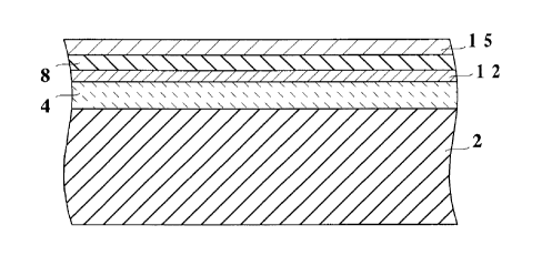
Fig. 1 shows the structure of a ferroelectric
capacitor fabricated in accordance with a first embodiment
of the present invention.. In the ferroelectric capacitor, a
silicon oxidation layer 4, a lower electrode 12, a
ferroelectric film (ferroelectric layer) 8 and an upper
electrode 15 are formed on a silicon substrate 2. The lower
electrode 12 is made of palladium oxide (PdOx), and the
upper electrode 15 is a~_so formed by palladium oxide (PdOx).
As shown in Fig. 11 which illustrates the
conventional ferroelectric capacitor, oxygen contained i.n
the ferroelectric film 8 passes through the platinum layer 6
having columnar crystal:. Palladium oxide is used for t:he
lower electrode 12 in the present embodiment. Since the
palladium oxide layer la? does not have columnar crystal:, it
is hard for the oxygen t:o pass through it. Therefore,
shortage of oxygen in the ferroelectric film 8 can be
prevented. Shortage of oxygen can also be prevented by the
upper electrode 15 which does not have columnar crystal~~.
Thus, the ferroelectric_Li~y of the ferroelectric film 8 is
improved. Remarkable irnprovement of ferroelectricity
CA 02197491 2001-04-30
9
degradation caused by u~,e of remanent polarization Pr is
observed when either of_ t:he upper electrode 15 or the lower
electrode 12 is made of_ palladium oxide in comparison with
when either one of the electrodes is composed of platinum.
Since both of th.e lower electrode 12 and the upper
electrode 15 are made of: palladium oxide in the embodiment
described above, the electrodes made of palladium oxide
ensure prevention of leakage of oxygen and Pb. Certain
prevention of leakage can be expected when either of the
electrodes is made of palladium oxide.
The ferroelectric~ capacitor described above can be
used for a nonvolatile memory when it is combined with a
transistor 24 as shown in Fig. 2.
Fig. 3A, Fig. 38, Fig. 3C and Fig. 3D show
successive stages in the fabrication of a ferroelectric
capacitor according to t:he present invention. A silicon
oxidation layer 4 is foz~med by carrying out thermal
oxidation of a surface of the silicon substrate 2 (Fig. 3.A).
In this embodiment, the :silicon oxidation layer 4 is formed
with a thickness of 600 nm. A palladium oxide formed on the
silicon oxide layer 4 bar reactive sputtering method using
palladium as a target i;~ defined as the lower electrode 12
(Fig. 3B). The lower a:'~ectrode 12 is formed with a
thickness of 200 nm.
A PZT film is formed on the lower electrode 12 as
the ferroelectric film f3 by sol-gel method (Fig. 3C). A
mixed solution of Pb (CH-:COO) ,~3H~0, 2r (t-OC9H5) ,~ and
Ti (i-OC3H~) 4 is used as a starter. The mixed solution i~;
dried at a temperature o.f 150 °C (hereinafter indicated in
Celsius) after carrying ~~ut spin coating, then pre-baking is
carried out at a tempera~ure of 400 °C for 30 seconds under
dried air atmosphere. ~fhermal treatment at a temperature
over 700 °C is carried out under O, atmosphere after carrzring
out the processes descr:i:oed for 5 times. Thus, the
3= ferroelectric film 8 having a thickness of 250 nm is formed.
In this embodiment, the PZT film is formed at a ratio of x
equals 0.52 in PbZruTi_.,0; (hereinafter the material is
CA 02197491 2001-04-30
indicated as PZT (52 ~ 48)).
Further, a layer of palladium oxide is formed on. the
ferroelectric film as the upper electrode 15 by reactive
sputtering method (Fig. 3D). The upper electrode 15 is
5 formed with a thickness of 200 nm. Thus, the ferroelect.ric
capacitor is completed. Any one of WOx, TiOx, TaOx, IrO~~,
Pt02, ReOx, RuOx, OsOx can be used for the palladium oxide.
In the case of forming a layer made of ferroelect:ric
substance on one of the oxidation layers, orientation of the
10 ferroelectric substance is degraded. In order to maintain
the orientation, the lager made of ferroelectric substance
can be formed on a conductive layer formed on the oxidation
layer. The conductive 7_ayer may be selected from of at
least one of the following: a W layer, a Ti layer, a Ta
layer, an Ir layer, a Pt: layer, an Ru layer, an Re layer, an
Os layer and the like. Further, leakage of the
ferroelectric substance can be decreased by providing the
conductive layer.
Fig. 4 shows they structure of a ferroelectric
capacitor fabricated in accordance with another embodiment
of the present invention. In this embodiment, a layer made
of titanium (having a thickness of 5 nm) is provided between
the lower electrode 12 c~Tld the silicon oxidation layer 9: as
a contact layer 30. In general, palladium oxide and silicon
oxide do not contact t:ic~htly with each other. Therefore,
there is a probability of degradation of ferroelectricit:y
occurring due to partia7_ delamination of a layer consisting
of an alloy of palladium oxide and silicon oxide. To
resolve the degradation, the titanium layer 30 which can be
contacted tightly with t:he silicon oxide layer 4 is provided
in this embodiment, so that the ferroelectricity is
improved. The titanium .Layer can be formed by sputtering.
Although the titanium layer is used as the contact
layer 30 in the embodiment described above, any other
materials which improve contact can be utilized. For
instance, a layer made of platinum can be used for the
contact layer.
CA 02197491 2001-04-30
11
Though the PZT film is used as the ferroelectric
film 8 in the embodiment. described above, any other
materials can be utilized as long as the materials are
ferroelectric _oxide. For_ instance, Ba~Ti~O,., can be used for
the ferroelectric film.
Fig. 5 shows the structure of a ferroelectric
capacitor fabricated in accordance with yet another
embodiment of the present; invention. A dielectric layer 90
having high dielectric constant is used for the
ferroelectric film 8 in this embodiment. The lower
electrode 12 made of pa7_ladium oxide is provided on the
silicon oxide layer 4, and a high dielectric thin film made
of SrTi03, (Sr, Ba)TiO, having perovskite structure is formed
thereon as the dielectric layer 90. In this embodiment,
ferroelectricity is improved in the same manner as in the
embodiment using the ferroelectric substance. In other
words, it is clear that t=he advantages offered by using the
ferroelectric layer can also be obtained by utilizing a
dielectric layer having high dielectric constant.
Fig. 6 shows the structure of a ferroelectric
capacitor fabricated in accordance with yet another
embodiment of the present invention. In this embodiment,
the silicon oxidation layer 4, the lower electrode 12, t:he
ferroelectric film (ferroelectric layer) 8 and the upper
electrode 15 are provided on the silicon substrate 2. The
lower electrode 12 cons_Lsts of a palladium layer 11 and a
palladium oxide layer 13 formed thereon. Also, the upper
electrode 15 consists o:= a palladium layer 7 and a palladium
oxide layer 9 formed thf=_:reon.
3C Fig. 7 is an en~-urged view of the vicinity of the
lower electrode 12. Since the palladium layer 11 has
columnar crystals, the oxygen contained in the ferroelectric
film 8 passes through the palladium layer 11. A palladium
oxide layer 13 is formed on the upper surface of the
3~, palladium layer 11 in this embodiment. Therefore, it i;~
possible to prevent shortage of oxygen contained in the
ferroelectric film 8 by forming the palladium oxide layer 13
CA 02197491 2001-04-30
12
as described above. The upper electrode 15 obtains the same
advantage which the lowe~x~ electrode 12 offers as described
above.
Since both of th.e palladium oxide layers are formed
in the lower electrode 1.2. and the upper electrode 15
respectively in this embodiment, it is possible to obtain a
ferroelectric capacitor having excellent ferroelectricity as
well as having less in:~Luences of aging. Certain advantages
as described above can be observed when either of the lower
electrode 12 or the uppE:r electrode 15 is formed by the
structure described abov=e .
Fig. 8A, Fig. BE~, Fig. 8C and Fig. 8D show
successive stages in thE> fabrication of the ferroelectri.c
capacitor described above. The silicon oxidation layer 4 is
formed by carrying out thermal oxidation of a surface of the
silicon substrate 2 (Fic~. 8A). In this embodiment, the
silicon oxidation layer 4 is formed with a thickness of 600
nm. The palladium oxide layer 11 is formed on the silicon
oxide layer 4 by utilizing palladium as a target (Fig. 8B).
The palladium oxide layE~r_ 13 is formed by carrying out a
thermal treatment at a temperature of 800 °C for one minute
under OZatmosphere. 'fhc~ palladium layer 11 and the
palladium layer 13 thus formed are defined as the lower
electrode 12. The lower electrode 12 is formed with a
thickness of 200 nm.
A PZT film is formed on the lower electrode 12 as
the ferroelectric film f3 by sol-gel method (Fig. 8C). A
mixed solution of Pb (CH:C.'00) ~~3H,0, Zr (t-OC4H5) ~ and
Ti(i-OC3H~)9 is used as a starter. The mixed solution i~~
dried at a temperature o:E 150 °C (hereinafter indicated in
celsius) after carrying out spin coating, then pre-baking is
carried out at a temperature of 400 °C for 30 seconds under
dried air atmosphere. ~Clzermal treatment at a temperatux-e
over 700 °C is carried out under O: atmosphere after carrying
out the processes descr_i.bed above for 5 times. Thus, the
ferroelectric film 8 having a thickness of 250 nm is formed.
In this embodiment, the :PZT film is formed at a ratio of x
CA 02197491 2001-04-30
13
equals 0.52 in PbZr~ Tii_h O, (hereinafter the material i~;
indicated as PZT (52 ~ 48)).
Further, the palladium 7 is formed on the
ferroelectric film 8 by sputtering method. Then, the
palladium oxide layer 9 is formed on a surface of the
palladium layer 7 by carrying out a thermal treatment at, a
temperature of 800 °C for one minute under O;, atmosphere
(Fig. 8D). The palladium layer 7 and the palladium oxide
layer 9 thus formed are defined as the upper electrode 1.5.
The upper electrode 15 i;~ formed with a thickness of 200 nm.
Thus, the ferroelectric capacitor is completed.
It is also preferable to form the contact layer 30
in the ferroelectric capacitor as described in Fig. 4.
The process which oxidizes a surface of the
palladium described above can be applied not only to the
ferroelectric film, but also to the dielectric layer having
high dielectric constant: described above, so that the same
advantages can be expected.
As described above, though leakage of oxygen can be
prevented by oxidizing t~lze surface of the palladium layer,
orientation of the ferroE=lectric layer is degraded by
formation of the pallad_i.um oxide on its surface. This
problem can be resolved by formation of at least one
conductive layer on the palladium oxide layer 13, selected
from a W layer, Ti laye,-, Ta layer, Ir layer, Pt layer, Ru
layer, Re layer, Os layf=:r or the like, as mentioned above.
The problem can also be :resolved by forming the lower
electrode as follows.
At first, a plat~:inum layer 80 (thin film conductive
substance) is formed very thinly on the palladium layer 11
as shown in Fig. 9. The platinum layer 80 is formed in a.
thickness of 30 nm. Ths=reafter, a thermal treatment is
carried out. The platinum layer is not oxidized because the
platinum layer 80 exposed on the surface does not react to
3~~ oxygen. Also, leakage of oxygen is shut out by formation of
palladium oxygen between crystals of the palladium layer 11
located under the plat.i:num layer 80 as a result of
CA 02197491 2001-04-30
14
oxidization of the crystals, because the platinum layer 80
is formed thinly. Therefore, the lower electrode 12 which
can shut out leakage of oxygen whilst maintaining good
orientation can be formed.
The palladium :~~~yer 11, being formed the thin
platinum layer 80 and trim being oxidized can also be u~>ed
as the lower electrode 7_2 by itself. The palladium layer 11
can be used as the conductive layer having good orientation
in the embodiment of improving orientation by providing a
conductive layer (a pal7_adium layer, a platinum layer and
the like) having good or-_Lentation in the palladium layer
formed by sputtering.
Also, all of the embodiments described in the above
can be applied not only t:o a ferroelectric capacitor using
the ferroelectric film but also to a capacitor using a
dielectric layer having high dielectric constant. Exactly
the same advantage offered by applying the present invention
to the ferroelectric fi7_m can be obtained when the present
invention is applied to t=he dielectric layer having high
dielectric constant.
LVhile the invention has been described in its
preferred embodiments, ~t is to be understood that the words
which have been used are words of description rather than
limitation and that changes within the purview of the
appended claims may be rnade without departing from the true
scope and spirit of the invention in its broader aspect~~.