Note: Descriptions are shown in the official language in which they were submitted.
2197975
- 1 - 95-PDC-176
UrfIVERSAL POWER MODULE
BACKGROUND OF THE INVENTION
Field of the Invention
This invention relates to a power supply for a power circuit and, more
particularly, to a power supply which generates a power output from one or
more input
power lines.
Background Information
Various electrical and electronic systems utilize control direct current
(DC) power derived from a variety of alternating current (AC) and DC input
line
voltages. For example, a nominal AC line voltage may be 110/120 VAC, 240 VAC,
480 VAC, or 575 VAC. Under normal operation, typical variations in these AC
line
voltages may present a wide range of possible input AC line voltages (e.g.,
about 60
through about 632 VAC). It is believed that such a wide voltage range has been
addressed by a variety of different power supply designs, or configurations
thereof,
each of which is associated with a subset of this range of possible AC line
voltages.
Furthermore, the AC line voltage may be single phase or plural phase
(e.g., three phases). Moreover, AC line voltages may have a wide frequency
range
(e.g., 40 through 400 Hz). DC line voltages, of course, have a zero frequency.
Prior art power supplies have typically addressed the variety of AC line
voltages with line frequency control power transformers and rectification
circuits.
However, such designs have been complicated by: (1) the variable number of
phases
(e.g., a single phase requires a greater volt-amp (VA) capacity while plural
phases
require plural transformer windings); (2) the variable line frequency (e.g.,~a
relatively
small change in line frequency from 60 Hz to 50 Hz requires about 16R~ more
transformer mass); and (3) the variable line voltage (e.g., multiple
transformer taps and
219797
- 2 - 95-PDC-176
associated jumpers are required). Furthermore, power transformers which input
the
AC line voltages preclude the input of a DC line voltage thereto.
Whenever surge waveforms must be suppressed from the line voltages,
a power supply design is further complicated. In typical power supply surge
tests, a
power supply must operate without failure or interruption of its output
voltage. The
ANSI C62.41 surge waveform, for example, includes a 6 KV peak open circuit
voltage
output from a 2 ohm voltage source with a 1.2 acs rise time and a 50 ~,s fall
time to
5090 of the peak voltage output, and with a 3 KA peak short circuit current
output with
an 8 acs rise time and a 20 acs fall time to 509'0 of the peak current output.
Although
a simple single phase power transformer may typically be protected from a
surge
waveform by the addition of extra transformer insulation, requirements for
plural
phases, plural taps and the requisite terminations thereto present further
opportunities
for arcing and damage by the surge waveform.
A power supply design is even further complicated when the surge
withstand capability requirement is coupled with the requirement for a wide
range of
line voltage magnitude and frequency. For line voltages having a possible 10:1
voltage
variation, the power dissipation in some components varies by a factor of
100:1. For
example, the power-up of a pulse-width modulation (PWM) controller is very
difficult.
If a resistor-zener combination is used to power the PWM controller, then a
100:1
change in power dissipation will occur at the resistor. In a circuit with a 5
KtI
resistor, a 10 V zener and a running bias of about 10 mA, for example, the
resistor
would dissipate about 0.5 W at a relatively low 60 VDC input line voltage.
However,
at a relatively high 600 VDC input line voltage, for example, the resistor's
power
dissipation would increase to about 70 W.
There is a need for an improved single power supply which accepts a
wide range of input line voltages.
There is a more particular need for such a power supply which accepts
both AC and DC input line voltages.
There is an even more particular need for such a power supply which
accepts a wide range of AC input line voltages over a wide range of line
frequencies
in addition to comparable magnitude DC input line voltages.
There is a still more particular need for such a power supply which
provides substantial protection from surge waveforms on the input line
voltages.
2197975
- 3 - 95-PDC-176
SUNINIARY OF THE I1WENTION
These and other needs are satisfied by the invention which is directed
to a power supply apparatus for converting at least one input voltage to an
output
voltage. The power supply apparatus includes a converting circuit for
converting the
input voltages to an intermediate voltage at a first node; a switching
regulator circuit
having a power voltage at a second node for providing a reference voltage
therefrom,
and for~providing a switching signal at a third node from the reference
voltage and a
feedback voltage; a circuit for electrically interconnecting the first node to
the second
node whenever the intermediate voltage exceeds a predetermined voltage; a
transformer
circuit including at least a primary winding electrically interconnected with
the first
node, and a seconda 'ry winding having a secondary voltage; a .feedback
circuit
cooperating with the transformer circuit for providing the feedback voltage
therefrom;
a switching circuit responsive'to the switching signal at the third node for
switching an
electrical current from the first node through the primary winding; and a
circuit
electrically interconnected with the secondary winding for converting the
secondary
voltage to the output voltage.
As another aspect of the invention, a power supply apparatus. for
converting at least one .input voltage to an . output voltage includes .a
first converting
circuit for converting the input voltages to a first intermediate voltage at a
first node;
a second converting circuit for converting the. first intermediate voltage to
a second
intermediate voltage at a second node; a switching regulator circuit having a
power
voltage at a third node for providing a reference voltage therefrom, and for
providing
a switching signal at a fourth node from the reference voltage and a feedback
voltage;
a circuit for electrically interconnecting the second node to the third node
whenever the
second intermediate voltage exceeds a predetermined voltage; a transformer
circuit
including at least a primary winding electrically interconnected with the
first node, and
a secondary winding having a secondary voltage; a feedback circuit cooperating
with
the transformer circuit for providing the feedback.voltage therefrom; a
switching circuit
responsive to the switching signal at the fourth node for switching an
electrical current
from the first node through the primary winding; and a circuit electrically
interconnected with the secondary winding for converting the secondary voltage
to the
output voltage.
2191975
- 4 - 95-PDC-176
BRIEF DESCRIPTION OF THE DRAWINGS
A full understanding of the invention can be gained from the following
description of the preferred embodiment when read in conjunction with the
accompanying drawings in which:
~ Figure 1 is a block diagram of a power supply in accordance with the
invention;
Figures 2A-2B, when placed side by side, are a schematic circuit
diagram of a power supply ip accordance with an embodiment of the invention;
Figures 3A-3B, when placed side by side, are a schematic circuit
diagram of a power supply in accordance with another embodiment of the
invention;
and
Figures 4A-4B, when placed side by side, are a schematic circuit
diagram of a power supply in accordance with another embodiment of the
invention.
DESCRIPTION OF THE PREFERRED EMBODIMENT
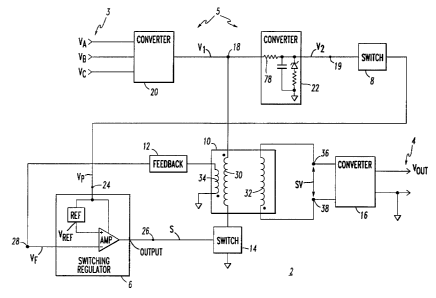
Referring to Figure 1, a block .diagram of a power supply 2 for
converting one or more input voltages V",VB,V~ at input terminals 3 to an
output
voltage Vou,. at output terminals 4 is illustrated. As described in greater
detail below
in connection with Figures 2A-2B, 3A-3B and 4A-4B the exemplary power supply 2
is suitable for providing a regulated DC output voltage from one or more of
the AC
or DC input voltages V", VH, V~ which exhibit a wide range of normal,
transient or
surge 'conditions such as, fvr example, an ANSI C62.41 surge waveform. The
power
supply 2 includes a converter 5, a switching regulator 6, a switch 8, a
transformer 10,
a feedback circuit 12, a switch 14 and a. converter 16, the operation of which
will be
more fully understood as described below.
The converter 5 converts the input voltages V,,, VB, V~ to an intermediate
voltage V, at node 18 and the intermediate voltage V, to another intermediate
voltage
V2 at node 19. The converter 5 includes converters 20,22 which respectively
convert
the input voltages V~,VB,V~ to voltage V,, and the voltage V, to voltage V2.
The
switching regulator 6 is powered at node 24 by voltage VP and provides a
reference
voltage V~, therefrom at output VREF of voltage reference REF. The switching
regulator 6 also -provides, at node 26, a switching signal S from output
OUTPUT
which is derived, in part, from the reference voltage V~, and a feedback
voltage VF
at node 28.
Z1~~9~
- 5 - 95-PDC-176
As explained in greater detail below in connection with Figures 2A-2B,
the switch 8 electrically interconnects node 19 to node 24 whenever the
voltage Vz
exceeds a predetermined voltage. The transformer 10 includes a primary
.winding 30,
a secondary winding 32 and a tertiary winding 34. One end of the primary
winding
30 is electrically interconnected with the node 18 and the other end is
electrically
interconnected with the switch 14. The switch 14, in turn, is, responsive to
the
switching signal S at the node 26 for switching an electrical current from the
node 18 '
through the primary winding 30. The tertiary winding 34 of the transformer 10
cooperates with the feedback circuit 12 and provides the feedback voltage VF
therefrom. The secondary winding 32 has a secondary voltage SV between nodes
36,38. The converter 16 is electrically interconnected with the secondary
winding 32
and converts the secondary voltage SV to the output voltage Vot,.,.,
Also referring to Figures 2A-2B, a schematic circuit diagram of an
exemplary power supply 40 is illustrated. The power supply 40 includes a
single phase
line voltage connection for the input voltages LINE,RETURN and the input
common
GROUND, and a three phase line voltage connection for the input voltages VA,
VB, VC
and the input common NEUTRAL. The GROUND and NEUTRAL input commons
are respectively connected to GND and ~ NEU ground signals. . Although the
GND,
NEU and GNDP signals are not interconnected in the exemplary embodiment, in a
three phase system with grounded neutral (not shown), the GND and NEU signals
are
connected at the power source (not shown). The GNDP signal changes with
respect
to the GND and NEU signals based on which one of the diodes 44,48,52,56,60 is
in
conduction.
As will be discussed more fully below, the power supply 40 accepts one
or more input voltages such as a single alternating current ~(AC) line voltage
for input
voltages LINE,RETURN; a single direct current (DC) line voltage for input
voltages
LINE,RETURN; or a three phase AC line voltage for input voltages VA, VB, VC
and
input common NEUTRAL. The exemplary single DC line voltage (e.g., a 300 VDC
bus) has a voltage range of about 85 VDC to about 900 VDC. The exemplary three
phase AC line voltage has a line-to-line voltage range of about 60 VAC to
about 632
VAC. Any of the AC line voltages (e.g., 50 Hz, 60 Hz) may have a frequency
range
of about 40 Hz to about 400 Hz. The exemplary single load voltage is a
regulated 24
VDC, 1 A, ~ 24 VA output suitable for powering any industrial load such as,
for
2197975
- 6 - 95-PDC-176
example, an electric power meter, an AC drive, a motor starter, a programmable
controller, or any other electrical or electronic load.
Any or all of the exemplary AC or DC line voltages may have an ANSI
C62.41 surge waveform as understood by those skilled in the art. An important
function of the power supply 40 is to continue operation during an ANSI C62.41
surge
test without failure and without interruption of the load voltage. As
explained below,
the capacitance of capacitor 115 at the primary winding 30 of the transformer
10 is '
smaller than the capacitance of bulk storage capacitor 122 on the secondary
side of the
transformer 10. In this manner, significant energy storage is provided on the
secondary side instead of the primary side of the transformer 10.
The power supply 40 includes the converters 5,20,22, switching
regulator 6, switch 8, transformer 10, feedback circuit 12, switch 14 and
converter 16
as discussed above in connection with Figure 1. The converter 20 provides the
voltage
V, at node 18 from one or more of the input line voltages LINE-
RETURN,VA,VB,VC. The input voltages LINE,RETURN, for either a single phase
AC or DC line voltage, are associated with a pair of series-connected diodes
42-44,46-
48 and a current limiting resistor 62,64, respectively. The input voltages
VA,VB,VC,
for a three phase AC line voltage, are associated with a pair of series-
connected diodes
50-52,54-56,58-60 and a current limiting resistor 66,68,70, respectively.
Fuses
72,74,76 protect the input power circuit associated with the input voltages
VA, VB, VC,
respectively. The voltage V, at node 18, as referenced from the ground signal
GNDP
at the anodes. of the diodes 44,48,52,56,60, is either a pulsating DC voltage,
a
r generally DC voltage with a three-phase ripple waveform, or a DC voltage
dependent
upon. whether the input line voltage is single phase AC, three phase AC, or
DC,
respectively. The diodes 42-44,46-48,50-52,54-56,58-60 of converter 20 provide
a full
wave rectification circuit for rectifying the AC line voltages to provide the
voltage V~
therefrom. The diodes 42-44,46-48 of converter 20 alternatively provide a
circuit for
sourcing the DC line voltage to the voltage V,.
The converter 22; which converts the voltage V, at node 18 ' to the
voltage VZ at node 19, includes resistors 78, 80, zener diode 82 and capacitor
84.
Under normal input line voltages, capacitor 84 is charged through resistor 78
to a
generally constant voltage determined by the predetermined zener voltage of
zener
diode 82 and the voltage drop across resistor 80, which is determined by the
zener
'~ 1 ~'~9~5
- 7 - 95-PDC-176
current of zener diode 82, the resistance of resistor 80 and the base-emitter
voltage of
transistor 85 (discussed below). Preferably, the resistor 78 has about a 3W
rating and
the zener voltage of zener diode 82 is about 24 V in order to accommodate the
exemplary wide range of AC and DC input voltages VA,VB,VC,LINE-RETURN.
~ With a suitable voltage at node ~ 19, the transistor 85 is turned on.
Subsequently, with sufficient emitter-base voltage developed across resistor
88 by
current flowing from node 19 through resistors 88 and 90 and through
transistor 85,
the series-pass transistor 86 sources current from node 19 through series-
connected
resistor 92 and diode 94 to node 24. This provides the DC voltage VP across
capacitor
96. The resistors 78, 80, zener diode 82 and capacitor 84 provide a circuit 97
for
detecting a predetermined voltage at node 19 and turning on the transistor 85
in
response to such predetermined voltage.
With a single phase DC line voltage, the converter 22 sources the DC
voltage at node 19 from the DC voltage at node 18. Similarly, with a three
phase AC
line voltage, the converter 22 sources the DC voltage at node 19 from the
generally
DC voltage at node 18. However, with a single phase AC line voltage, the
operation
of the converter 22 and the switch 8 depends upon the magnitude of the single
phase
AC line voltage. Under very low line conditions with respect to the normal
operating
input voltage range of the power supply 40, the transistors.85,86 are not
turned on and
no current is sourced to node 24. Under generally nominal line conditions,
transistors
85, 86 are always turned on and current is sourced to node 24 to maintain the
voltage
VP as regulated by zener diode 98 and filtered by capacitor 100. Under certain
low
line conditions, transistors 85,86 are momentarily turned on by the peak
voltage at
node 18 and are otherwise turned off.
The transistors 85,86 form a latching circuit having a first state
whenever the voltage VZ exceeds a first predetermined voltage and a second
state
whenever the voltage VZ falls below a .second predetermined voltage which is
lower
than the first predetermined voltage as determined by the feedback ~ resistors
102,104
in conjunction with the resistor 80. The transistor 86 is responsive to the
transistor 85
which, in turn, is responsive to the detection circuit 97. The transistor 85
is fumed on
about when the circuit 97 detects the first predetermined voltage at node 1.9.
In turn,
the transistor 86 is turned on~ by the transistor 85. In the first ("on")
state, the node
19 is electrically interconnected with the node 24 in response to a suitable
input line
2191°l
- g - 95-PDC-176
voltage. In the second ("off') state, in response to an undervoltage condition
of the
input line voltage, the node 19 is electrically disconnected from the node 24.
Subsequently, however, the transistor 86 electrically reconnects the node 19
to the node
24 in order to recover from the undervoltage condition whenever the voltage VZ
exceeds the first predetermined voltage. The diode 94 prevents discharge of
the
voltage VP through the switch '8 and, also, as discussed below, permits a
separate
charging path from the tertiary winding 34 of the transformer 10. During
normal
operation of the switching regulator 6, the voltage VP at node 24 is
maintained by
current from the tertiary winding 34, except during about the time of zero
crossings
of a single phase AC line (e.g., input VA, VB or VC). During such time, the
capacitor 100 ritaintains the voltage Vp to a suitable level. At startup, in
the first state,
the diode 94 electrically interconnects the voltage VZ to the voltage Vp.
Following
startup, the separate charging path froth the tertiary winding 34 of the
transformer 10
predominates with the diode 94 generally sourcing negligible current.
Current flowing through the resistor 78 charges the capacitor 84, in the
"off" state of the transistors 85,86, to a voltage (e.g., about 25 VDC)
determined
primarily by the zener diode 82 and, also, by the base-emitter voltage of the
transistor
85. On the other hand, in the "on" state, the capacitor 84 is electrically
interconnected
with the node 24 by the transistor 86, the voltage of the capacitor 84
generally follows
the line voltage at node 18,-and the capacitor 84 is discharged through the
transistor
86 and the resistor 92. Under relatively low input line conditions, a startup
delay of
about.15 seconds in the transition from the "off" state to the "on" state is
provided by
the capacitor 84.
An important feature of the present invention is an automatic restart
feature provided by the switch 8. This feature is critical in the event of a
relatively
low input line condition for a single phase AC line. Under normal operation,
with a
three phase AC line or a single phase DC line, the switch 8 will normally
always latch.
However, with a relatively low condition of a single phase AC line, the switch
8 may
not latch immediately. In this case, especially with a single phase AC line
voltage of
about 55-60 VAC, the switch 8 may unlatch and re-latch one or more times
before
normal operation of the switching regulator 6 is provided. .
Resistors 102,104 form a feedback circuit 105 from the collector (output)
of the transistor 86 to the base (input) of the transistor 85. The transistor
86
2197975
- 9 - 95-PDC-176
electrically interconnects the voltage VZ at node 19 to the voltage VP at node
24
whenever the voltage VZ exceeds the first predetermined voltage and
electrically
disconnects the voltage VZ from the voltage VP when the voltage VZ falls below
the
second predetermined voltage, with sufficient hysteresis preferably provided
to prevent
spuribus switching between the first and second states. Capacitors 106,108
speed the
latching of the transistors 85,86 in the first ("on") state.
The tertiary winding 34 of the transformer 10 has an AC tertiary voltage
VT, positive cycles of which supplement the charge of capacitors 96,100 and,
hence,
the voltage Vp with current fed by diode 110 through resistor 112 of the
feedback
circuit 12. The secondary winding 32 of the transformer 10 has an AC secondary
voltage VS, positive cycles of which charge the capacitor 114 as rectified by
a flyback
diode 116. The voltage across the capacitor 114, in turn, is filtered by
inductors
118,120 and .the output capacitor 122. The output voltage Vow. and the output
common NEUTRAL-O of the power supply 40 are obtained from opposite sides of
the
capacitor 122 and provide a single load voltage connection. Preferably, the
capacitance
of the capacitor 122 on the secondary side of the transformer 10 is greater
than the
capacitance of the capacitor 115 at the primary winding 30. The capacitor 115
filters
and shapes the voltage V,. The capacitor 122 provides bulk storage to maintain
a
suitably constant output voltage Vo~,.,.. In this manner, bulk storage
capacitance is
provided for a relatively constant, DC voltage (e. g. , Vo".,.) rather than a
voltage (e. g. ,
V,)~ which has relatively wide voltage and frequency ranges. Furthermore, with
a
relatively small value of capacitance of the capacitor 115 with respect the
relatively
large value of capacitance of the capacitor 122, the c~nacitor 115 is more
readily
protected from transients or surge conditions.
. In the exemplary embodiment, during single phase AC line zero
crossings at low voltage (e. g. , at about 60 VAC), the capacitor 115 (e. g. ,
about 0.22
~cE) does not maintain sufficient charge to power the primary 30. However, the
capacitor 100 (e.g., about 10 ~cF) suitably maintains control power for the
switching
regulator 6 and the capacitor 122 (e.g., about 3300 ~cF) suitably maintains
the +24
VDC output voltage Vou,...
The feedback circuit 12 also includes a rectification circuit .128 having
diode 130, resistor 132 and capacitor 134, and a divider circuit 135 having
resistors
136 and 138. The rectification circuit 128 rectifies the tertiary voltage VT
and
219791
- 10 - . 95-PDC-176
produces an intermediate feedback voltage V,~ therefrom at node 139. In turn,
the
divider circuit 135 produces the feedback voltage VF, at input FDBK of the
switching
regulator 6, from the intermediate feedback voltage V,F.
The switch 14 includes a switching transistor 140, such as the exemplary
insulated gate bipolar transistor, interconnected with the primary winding 30
of the
transformer 10. The node 26 having the switching signal S is electrically
interconnected with the gate of the transistor 140 by resistor 142. The
primary current
IP of the primary winding 30 flows through the transistor 140 whenever it is
turned on
by the true or on-state of the .switching signal S. The primary current Ip, in
turn, is
conditioned by a conditioning circuit 144 which develops a current sense
signal V, at
input CS of the switching regulator 6. In addition to the feedback voltage VF
discussed
above, the switching regulator 6 also derives the switching signal S, in part,
from the
reference voltage V,~ and the current sense signal V,.
During initial startup of the exemplary switching regulator 6, the current
sense input CS limits the primary current IP which is required to establish
the
appropriate secondary voltage VS of the secondary winding 32. Subsequently,
under
abnormal operating conditions, the current sense input CS facilitates short-
circuit
protection and limits the primary current IP to a suitable value. Otherwise,
the FDBK
input of the switching regulator 6 dominates under normal operating
conditions. The
ezemplary switching regulator 6 (as well as the switching signal S and
switching
transistor 140) operate at about an exemplary 10 kHz switching frequency which
is
established at a CT input thereof, although the invention is applicable ~o any
switching
frequency. The switching regulator 6 also has a CP input which provides
suitable
compensation for an error amplifier AMP (shown in Figure 1) which compares.the
reference V~ and feedback VF voltages.
The conditioning circuit 144 includes resistors 146,148,150. The
primary current Ip, which flows through the transistor 140 when the switching
signal
S is active, produces an intermediate current sense voltage Vv across the
resistor 146.
In turn, the resistors 148,150 form a divider circuit 151 which produces the
current
sense signal V, from the intermediate current sense voltage VQ. Whenever the
transistor 140 is turned off, the primary current IP is alternatively directed
by a diode
circuit 152 to a snubber circuit 154, thereby eliminating the stray energy
from the
transformer 10 and the transistor 140.
219797
- 11 - 95-PDC-176
The converter 20 also includes a surge suppression circuit 156 for
suppressing an ANSI C62.41 surge waveform from the intermediate voltage V, at
node
18. The circuit 156 includes the series resistors 62,64,66,68,70, which limit
the
current through each respective pair 42-44,46-48,50-52,54-56,58-60 of the
diodes 42-
60, tlfereby protecting such diodes from overcurrent; the capacitor 115, which
shapes
the surge waveform at the node 18; and three series metal oxide .varistors
(MOV's)
158,160,162, which operate in conjunction with the series resistors 62-70,
clamp the
voltage of the surge waveform between the node 18 and the~ground GNDP, and
protect
the capacitor 115 and the diodes 42-60 from overvoltage.
The power supply 40 also includes additional surge suppression circuits
164,166,168,170,172,174. Circuit 164 includes a divider 175 having resistors
176,178
with .an output 179; an operational amplifier 180; and a transistor 182. The
negative
(-) input of the operational amplifier 180 is connected to the VREF output of
the
switching regulator 6 and is referenced to the reference voltage V,~. The
positive (+)
input of the operational amplifier 180 is connected to the output 179 of the
divider 175
which provides an attenuated version of the intermediate voltage V, at node
18.
Whenever a surge voltage causes the intermediate voltage V, to exceed a
predetermined
voltage, as determined by the reference voltage V,~ and the preselected values
of the
resistors 176,178, the output 181 of the operational amplifier 180; which is
connected
to the base of transistor 182, turns on the transistor 182. The collector of
the transistor
182 is connected to the gate of~ the transistor 140. Whenever the transistor
182 is
turned on, the transistor 140 is turned off, thereby protecting the transistor
140 from
an excessive surge current which would have been caused by the surge voltage
and,
also, keeping the transistor 140 within its safe operating area.
Circuit 166 includes three series bi-directional zener diodes 184,186,188.
The circuit 166 is connected between the collector and emitter of the
transistor 140 and
protects such transistor from an excessive surge voltage.
Circuit 168 is a zener diode which protects the output OUTPUT of the
switching regulator 6 from an excessive feedback voltage (from current IP
through the
resistor 146) which causes current to flow through the anode of diode .190,
through
resistor 142 and into the cathode of zener diode 168. Such excessive feedback
can
occur during ANSI C62.41 type transients.. Circuit 170 includes zener diode
190 in
parallel with gate-emitter resistor 192. The zener diode 190 protects the gate-
emitter
X197975
- 12 - 95-PDC-176
junction of the transistor 140 from transients in the zener mode of the diode
190, and
from excessive reverse gate-emitter voltage in the diode mode when the
transistor 182
is turned on. The transistor 140 is also protected by the inductance of the
primary
winding 30 of the transformer 10 along with the resistance of the resistor
146.
- Circuit 172, which includes zener diode 194 and capacitor 196, reduces
the impact of transients and protects the input CS of the switching regulator
6 from an
excessive surge voltage at the intermediate voltage V, coupled from node 18
through '
the primary winding 30 of the transformer 10 and through the transistor 140
into
resistor 146. The zener diode 194 protects the input CS from daniage caused by
an
excessive feedback voltage V,.
Circuit 174 includes four series zener diodes 198,200,202,204 which
clamp or limit the surge voltage and other transients of the intermediate
voltage V,
coupled from node 18 through the secondary winding 32 of the transformer 10
and
through the converter 16 to the output voltage Vo".,.. Otherwise, under normal
operation, the circuit 174, like the circuits 166,168, is an open circuit.
Figures 3A-3B illustrate another power supply 206 which is similar to
the power supply 40 of Figures 2A-2B. The power supply 206 includes a three
phase
line voltage connection for the input voltages VA,VB,VC and the input common
NEUTRAL. The three phase AC line voltage has a line-to-line voltage range of
about
90 VAC to about 600 VAC. Any of the AC line voltages may have a frequency
range
of about 45 Hz to about 66 Hz. The exemplary single load voltage is a
regulated 24
VDC, 1 A, 24 VA output suitable for powering any industrial load such as, for
example, an electric power meter, an AC drive, a motor starter, a programmable
controller, or any other electrical or electronic load.
A low pass filter 210 including inductor 212 and capacitor 214 provides
further shaping of the surge waveform between node 18 and node 215 at resistor
78.
Inductor 216, connected between node 215 and ' the primary winding 30 of the
transformer 10, limits the current from the node 18 to the switching
transistor 140.
Capacitor 218 provides further shaping of the voltage V,P at the primary
winding 30.
Capacitor 218 is protected by the MOV's 158,160,162, the low pass filter 210
and the
inductor 216.
A zener diode circuit 220, including three series zener diodes
184',186',188', limits the voltage across the primary winding 30 of the
transformer 10
219191
- 13 - 95-PDC-176
and the switching transistor 140. In this manner, the circuit 220, the
impedance of the
primary winding 30 and the resistance of the resistor 146 protect the
switching
transistor 140 from surge voltages and transients. Zener diode 222 protects
resistor
146 and the CS input of the switching regulator 6. The zener diode 222, which
is in
series with the circuit 220, also limits the voltage V,p and further protects
capacitor
218.
Positive temperature coefficient (PTC) resistive element 224 limits the -
current between the input common NEUTRAL and the ground signal NEU. The three
series MOV's 158,160,226, which operate in conjunction with the series
resistors 66-
74, clamp the voltage of the surge waveform between the node 18 and the ground
signal NEU. Low pass filter 227, including inductor 228 and capacitor 230,
prevent
radio frequency interference (RFI) from being coupled back to the input
voltages
VA,VB,VC. The capacitor 106 speeds the latching of the transistors 85,86 in
the first
("on") state. The capacitor 108' slows the response of transistor 86 to
prevent spurious
transitions caused by noise or surge transients at node 19.
A switching frequency modulation circuit 231 includes the resistor 232,
zener diode 234, diode 236 and capacitor 238 connected between, the tertiary
winding
34 of the transformer 10 and the CT input of the switching regulator 6. Under
relatively high input voltage conditions (e.g., at about greater than 300 V),
the
modulation circuit 231 modulates the CT input of the switching regulator 6 in
order to
decrease the frequency of the switching signal S. This is significant, Because
at high
voltages, the switching transistor 140 has a. larger switching loss and a
shorter on-state
time. By reducing the switching frequency, power losses in the switching
transistor
140 are reduced which improves the efficiency of the power supply 206 at
relatively
high input voltage conditions.
When the switching transistor 140 is turned on, the voltage of the
tertiary winding 34 is proportional to the voltage of the secondary winding 32
of the
transformer 10. (which establishes the DC voltage Vow. through the diode 116).
On the
other hand, when the switching .transistor 140 is turned off, the voltage of
the tertiary
winding 34 is proportional to the voltage of the primary winding 30 (which
follows the
intermediate voltage V,P and the input voltages V",VB,V~. The diode 236 and
capacitor 238 determine a negative voltage across the capacitor 238 which is
proportional to the input voltages V", VB, V~. About when the magnitude of the
voltage
21919?~
- 14 - 95-PDC-176
across the capacitor 238 exceeds the zener voltage of zener diode 234,
resistor 232
removes charge from capacitor 239 at the CT input of the switching regulator
6,
thereby decreasing the switching frequency. Otherwise, at relatively low input
voltage
conditions (e.g. , less than about 300 V), the switching frequency of the
switching
regulator 6 is not modulated by the modulation circuit 231.
Figures 4A-4B illustrate another power supply 240 which is similar to
the power supply 40 of Figures 2A-2B and the power supply 206 of Figures 3A-
3B.
The power supply 240 includes a single phase line voltage connection for input
voltages
LINE, and input common GROUND. The single phase AC or DC line
voltage has an AC voltage range of about 96 VAC to about 264 VAC or a DC
voltage
range of about 100 to about 350 VDC. The AC .line voltage may have a frequency
range of about 45 Hz to about 66 Hz. The exemplary single load voltage is a
regulated
24 VDC, 1 A, 24 VA output suitable for powering any industrial load such as,
for
example, an electric power meter, an AC drive, a motor starter, a programmable
controller, or any other electrical or electronic load.
MOV 242,.which operates in conjunction with the series resistors 62,64,
clamps the voltage of the surge waveform between the node 18 and the anodes of
the
diodes 44,48, and protects the capacitor 115 and the diodes 42-48 from
overvoltage.
The MOV 244 similarly limits the voltage between the input common GROUND and
the anodes of the diodes 44,48. Low pass filter 227', including inductor 228
and
capacitor 230', prevent radio frequency interference (RFn from being coupled
back to
the input voltages VA,VB,VC. .
A low pass filter 210' provides further, shaping of the surge waveform
between node 18 and node 215 at resistor 78. The filter 210' includes a first
series
low pass filter 245, having inductor 246 and capacitor 248, and a second
series low
pass filter 249, having inductor 250 and capacitor 252.
Circuit 166" includes two series zener diodes 184",186". The circuit
166" is connected between the collector and emitter of the transistor 140 and
protects
such transistor from an excessive surge voltage.
While specific embodiments of the invention have been described in
detail, it will be appreciated by those skilled in the art that various
modifications and
alternatives to those details could be developed in light of the overall
teachings of the
disclosure. Accordingly, the particular arrangements disclosed are meant to be
2~'~~'~7~-
- 15 - 95-PDC-176
illustrative only and not limiting as to the scope of the invention which is
to be given
the full breadth of the appended claims and any and all equivalents thereof.