Note: Descriptions are shown in the official language in which they were submitted.
2~98002
WO 96/07084 PCT/DE95/01150
Docket MAYFR 0183
Translation of German text
DESCRIPTION
Circuit for Setting the Operating Point of an Opto-Electronic
Component
_
FIELD OF INVENTION
The invention concerns a circuit for setting the operating
point of a photodiode according to the Preamble of the Claim 1.
PRIOR ART
A circuit of this type is known, for example, from the DE
- C 39 30 415 and is used to measure changes in the light
incidence and to obtain usable signals from this. Since there
is on principle a logarithmic connection between the intensity
of illumination and the no-load voltage of a photodiode, a
saturation voltage is quickly reached with increasing
illumination, which is reached at approximately 0.5 V,
depending on the photodiode used. Above this saturation
voltage, there is a linear relation between illumination
intensity and photoelectric current over many powers of ten.
If the intent is to convert alternating light wanted signals,
superimposed by constant light, into a signal voltage, it is
necessary that the photodiode be operated in a range below this
2 1 98û~2
W0 96/07084 PCT/DE95/01150
saturation voltage in order to be able to detect a signal
pattern at all and thus set the operating point.
In the DE-C 39 30 415, a compensation voltage is generated
for this by means of a second photodiode without requiring
current from the supply voltage. The voltage from this second
photodiode is supplied to the actual photodiode as counter- or
external voltage via a coil with constant internal resistance.
As a result of this, two photodiodes are initially necessary,
of which only one actively receives the alternating light.
However, for a compensation of the photoelectric voltage with
the same type of voltage generated by the second photodiode,
both diodes must be illuminated evenly, which is not always
ensured. In order to solve this problem, it is suggested that
the interference signal photodiode is designed larger than the
wanted signal photodiode, which results in higher costs for the
circuit. In this case, the voltage is varied while the
resistance remains the same. The use of a coil as direct
current path additionally has the disadvantage that this
circuit cannot be integrated into an IC (integrated circuit).
In addition, this integration is made even more difficult here
in that it is not possible to switch to a symmetric input
because of the capacitor, which is parallel-connected to the
interference signal photo sensor.
2 1 q80~2
,
From the DE-A 32 33 728 we are familiar with a circuit
arrangement for suppressing constant light signal components in
a pre-amplifier for an infrared-light receiver with a
photodiode, for which the operating point is fixed by a series-
connected resistor. In order to keep the current consumptionof the photodiode low and to ensure an effective constant light
- suppression during the signal processing, as well as to reach
a high-ohmic input stage, a diode through which off-state
current from the photodiode flows is connected parallel to the
resistor that determines the operating point for the
photodiode, and the received signal is transmitted to an
impedance converter with bootstrap layout, which operates
jointly with a following amplifier stage as a cascaded circuit.
Thus, the circuit arrangement can change the load resistance of
the photodiode without loop, depending on the constant light
component, and can thereby free the wanted signal that can be
tapped from direct current components. However, an additional
operating voltage is still always required.
ALTERED PAGE 2 ov
21 98002
WO 96/07084 PCT/DE95/01150
In order to hold the photodiode below the saturation
voltage, it is also known to operate the photodiode during the
diode operation with bias voltage. For this, a bias voltage is
fed to the diode in order to block it (opposite polarization to
the saturation voltage). Alternatively, the diode can also be
- operated by a cell without bias voltage. In that case, the
photodiode functions as current source. For this, the
photodiode is kept at a zero potential wile the photoelectric
current is compensated via a resistor.
Both types of operation, meaning diode or cell operation,
have in common that they need an external power source in order
to compensate for the photoelectric current that appears during
illumination. Depending on the type of diode and illumination,
this compensation current can amount to several umpteen ~A to
lS several mA. This current must be taken from the supply
voltage, which can lead especially with battery operation to a
quick failure of the battery. This current, which must be
supplied by the battery, can possibly amount to a multiple of
the current taken up by the complete circuit.
The invention is suited in a preferred way for use in
connection with a battery-operated water sensor, such as is
known from the DE-U 93 09 837.5. Operating a water sensor with
a battery is desirable, for example, in the field of boat
construction. Boats of "leisure time captains" as a rule have
21 q8002
~0 96/07084 PCT/DE95/01150
one or several sleeping berths in the bow, below the sliding
window on the side. Frequently, someone neglects to close
these, so that spraying water wets the sleeping berths without
the boat coxswain noticing it. If in this case the window
surfaces are checked at regular intervals for spraying water
-- with the known water sensors, then these can be closed, if
necessary automatically. Another area of use would be, for
example, a water sensor attached to the clothes line of a
housewife, which sounds a signal when rain drops appear. Here
too it is necessary to check for water drops that appear. Such
devices therefore basically do not depend on an external
current supply, but if they are operated with a 9 V unit, the
average power consumption must be kept low. They can generally
be used wherever alternating light wanted signals are detected.
;
DISCLOSURE OF THE INVENTION
Starting with this Prior Art, it is therefore the object
of the invention at hand to generate the compensation current
needed due to the constant light current without external
voltage, so that almost no current must be supplied by the
power supply or battery.
This problem is solves with the features in Claim 1.
With the opto-electronic elements for receiving the light
signals, regardless of whether photodiodes, light diodes or
21 98002
phototransistors are used, the voltage in this case also
increases logarithmically with the illumination intensity until
the saturation voltage is reached at, for example, 0.5 V. In
the saturation voltage range, a further increase in the
illumination intensity does not lead to a further voltage
increase, meaning a small alternating light component (LED
modulation) does not have any effect on the output voltage. An
alternating current can form only in the characteristic
curvature range. For that reason, the voltage at the opto-
electronic element must be held to a value below the saturationvoltage. The simplest way to do this is with a load resistor,
which uses enough current so that the voltage at the opto-
electronic element, for example, always amounts to half the
saturation voltage. No external current is necessary for this,
but the resistor must be adjusted constantly to the constant
light or environmental light intensity. For example, for U/2
of the saturation voltage, an alternating light component will
always cause a voltage change at the resistor as well.
Other advantages follow from the dependent claims.
SHORT DESCRIPTION OF THE DRAWINGS
Fig. 1 A circuit where a germanium diode with load
resistor is parallel-connected to a photodiode;
ALTERED PAGE 5
21 q8002
Fig. 2 A circuit where two photodiodes, a Schottky or
a silicone diode are parallel-connected with a
load resistor;
Fig. 3 A circuit where a photodiode is parallel-
connected to a field effect transistor;
Fig. 4 A circuit according to Fig. 2 with symmetric
operational amplifier;
Fig. 5 A circuit according to Fig. 1 with a symmetric
operational amplifier;
10 Fig. 6 A circuit according to Fig. 2 with an
asymmetric amplifier circuit;
Fig. 7 A circuit where a controllable field effect
transistor, which can be controlled via an
operational amplifier, is connected between two
photodiodes;
Fig. 8 A circuit where a light-emitting diode is used
as opto-electronic element.
PREFERRED EMBODIMENTS OF THE INVENTION
The invention is explained in more detail with an example
and by referring to the enclosed drawings. However, the
exemplary embodiments are simply examples, which are not
ALTERED PAGE 6
21 ~8002
designed to limit the inventive concept to a specific physical
arrangement.
The circuit is designed to adjust the operating point of
at least one opto-electronic element, wherein the opto-
electronic element is a component of a receiver for alternating
- light wanted signals with superimposed constant light signals.
Known photodiodes 10, lO', 10 ", but also light diodes 110 can
function as opto-electronic element. Essential is only the
quality of functioning as receiver, which is on principle
possible with a light-emitting diode. All circuits, however,
have the problem that the opto-electronic elements can convert
alternating light into useful output signals only within a
specific range. It is therefore necessary to hold the
operating point for these opto-electronic elements below the
saturation voltage, which is done with a resistive circuit with
automatic control resistance. In the resistive circuit, the
resistance is controlled depending on the voltage and, if
necessary, also depending on the frequency, so that a voltage
develops at the opto-electronic element, which is in the range
of a preferably positive voltage below the saturation voltage.
ALTERED PAGE 7
21~8002
~o 96/07084 PCT/D~95/01150
Photodiodes 10, 10', 10 " are used as opto-electronic
elements in the Figures 1 to 7 and a light-emitting diode 11
is used in Figure 8.
In Figure 1, the photodiode 10 is subjected to an
illumination L. A diode 11 is arranged parallel to the
photodiode, which in this case is a germanium diode. Connected
in series with this germanium diode is a small load resistor
of about 10 kilohm. With increasing voltage of the photodiode,
the germanium diode opens up at about 0.3 V, so that the
photodiode is stressed only if a photoelectric voltage > 0.3 V
appears. In that case, the PY~nc~ voltage can then be
discharged via the resistor 12 because the internal resistance
of the germanium diode changes in depPn~Pnce on the
photoelectric voltage. The resistance functions to prevent
signal asymmetries for high illumination densities (rectifier
effect). The disadvantage of this circuit is that germanium
diodes are rarely used, so that a relatively expensive circuit
results in this case.
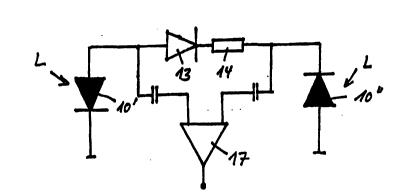
In Figure 2, two photodiodes 10', 10'' provide a combined
positive and negative voltage of ma~ r lV when illuminated.
A Schottky diode 13 (e.g. BAT 83) with a forward voltage of 0.4
V limits the photoelectric voltage to 0.2 V per photodiode.
ALlERE~ PAG~
2 1 98002
The same result can be obtained by using a silicon diode (lN
41/48) with a forward voltage of about 0.6 V. In this case,
twice the output voltage is an advantage while the use of two
photodiodes is a disadvantage. As for the exemplary embodiment
in Figure 1, the Schottky diode 13 opens up when the forward
_ voltage is reached, so that the resistor 14 of, for example, 2
kilohm can discharge the excess photoelectric voltage. It is
also possible to omit the resistors 12, 14 in the exemplary
embodiments shown in Figures 1, 2, insofar as the internal
resistance of the diode 11 or the Schottky diode 13 is
sufficiently high.
In the exemplary embodiment for Figure 3, for example, a
field effect transistor 15 is connected parallel or is added to
the photodiode 10 that is subjected to an illumination L. The
photodiode voltage is compared constantly to a reference
voltage via an operational amplifier 16 and is adjusted by way
of a field effect transistor. The field effect transistor
functions as variable resistor. In this case, the drain source
or the collector-emitter resistance is adjusted such that the
voltage at the opto-electronic element remains below the
saturation voltage or corresponds to about half the saturation
voltage. The advantages of this circuit are that only one
photodiode is required and that the control is also very exact.
The disadvantage is that the operational amplifier requires
ALTERED PAGE g
2 1 98002
current. However, since inertial operational amplifiers are
preferably used in this case, the operational amplifier only
requires a current of about 1.2 ~A. Optional bipolar
transistors or other semiconductor elements can be used in
place of the field effect transistor 15. However, the latter
require a low base current.
- The circuits for the Figures 1 - 3 can also be operated
with a symmetric operational amplifier. This is shown for the
exemplary embodiment of Figure 2 in Figure 4 and for the
exemplary embodiment of Figure 1 in Figure 5. In this case,
the operational amplifier is added as symmetric amplifier.
Common-mode interferences are suppressed by this. The
operational amplifier 17 is connected via capacitors parallel
to the germanium diode 11 or the Schottky diode 13 and the
coordinated resistors 12, 14. Figure 6 shows a simplified
version of the aforementioned circuits in that an asymmetric
amplifier 28 is used.
An optimum, but somewhat more expensive solution is shown
in Figure 7. For the photo diode current control, a field
effect transistor 18 is arranged in series between two unipolar
photodiodes 10', 10 ". An operational amplifier 19 is arranged
parallel to the field effect transistor. Resistors 20, 21,
which are bridged via capacitors 22, 23, are arranged between
the photodiodes and the operational amplifier. The resistors
ALTERED PAGE 10
2 1 980Q2
only function to compensate the positive or negative
photoelectric voltage to the operational amplifier, so that for
a positive photoelectric voltage of, for example, 0.2 V and a
negative photoelectric voltage of 0.2 V, the operational
amplifier always has 0 plus 0 V. With this, the operational
amplifier 19 can control the photodiode current via the field
- effect transistor. The capacitors 22, 23 function to bridge
the alternating voltage, so that the operational amplifier 19
can additionally be used as first alternating light signal
amplifier stage. The share of direct current is coupled out
via the capacitor 29, while the photodiode current is
controlled via the line 30. The alternating current is finally
suppressed with the components 31 and 32.
All circuits have in common that the photodiode is
dynamically stressed, without current being drawn in
considerable amounts from the power supply. Without
-
illumination, the photodiode and, if existing, the load diodes
or resistors are high-ohmic (or high-ohmic current sources).
When subjected to illumination, the photodiode as generator as
well as the load diodes or resistors become low-ohmic, that is
always in such a way that the internal resistance of the
photodiodes is compensated for by an equally high internal
resistance of the load diodes or resistors. (Exemplary
embodiments of Figures 1, 2, 4, 5.) As a result of this, an
output signal is always ensured, even if the external light
ALTERED PAGE 11
2 1 9800~
share is high. Besides, the alternating light wanted signal
that must be detected to generate the output signal is for the
most part low in relation to the constant light of the external
illumination, regardless of which application range of the
wanted signal this concerns.
For one practical application, it has turned out that with
- a standard wiring and with full insolation, a current of 260 ~A
flows, which must be compensated with a countervoltage or
current. This compensating current is in any case higher than
is feasible with constant battery operation. For the mentioned
exemplary embodiments (for which a downstream connected, low
current operational amplifier takes over the task of control
voltage generation for the field effect transistor as well as
functions simultaneously as alternating voltage amplifier), an
average current consumption with high sensitivity and discrete
amplifier in C-Mos Technology of 10 ~A for the complete water
sensor could be achieved. If we also include the high current
for the rather seldom occurring alarm case, then a commercially
available 9 V unit can last more than 2 years.
Light-emitting diodes can also be used as alternative for
the photodiodes, but for the same purpose. In contrast to the
known photodiodes, the light-emitting diodes have the advantage
that they can on principle be acquired much cheaper. They
supply between 0.9 V and 2 V as saturation voltage and can be
2S stressed with a simple bipolar transistor 113, which is
ALTERED PAGE 12
2 1 98002
-
connected via a resistor 111 and a capacitor 112 preferably to
a symmetric circuit. Figure 8 shows that the transistor is
connected parallel to the light-emitting diode 110. The
transistor base point is connected between a resistor 111 of
330 kilohm and a capacitor 112 of 10 nF. The base collector
path in this case is linked to the light-emitting diode 110 and
- the base emitter path with the off-state side of light-emitting
diode 110. A BC 548 can be used as transistor. The
operational amplifier 114 shown here with dashed line, for
example, can be provided since a symmetric wiring results in
this case.
Alternatively, the same goal can also be reached with the
photodiode path of a phototransistor, provided the base
collector path is incorporated into the control circuit.
However, this phototransistor path then functions again as a
photodiode.
-
All the circuits have the advantage of not having anycoils and thus can be easily integrated into an IC (integrated
circuit). In addition, they can all be laid out in such a way
that they can be connected to a symmetric input. Even if more
than one photodiode is needed as opto-electronic element, as
for the exemplary embodiment in Figure 2, it is still not
necessary to design these photodiodes differently at
considerable expense since they can also receive uneven amounts
of light without endangering the function of the circuit. The
ALTERED PAGE 13
21 98Q02
load control occurs exclusively for constant light signals,
while alternating light signals are purposely suppressed during
the load control. The opto-electronic elements used,
photodiode 10, 10', 10'' and light-emitting diode 110 as well
as the base collector path for the phototransistor represent
opto-electronic elements that generate current during the
- short-circuit operation and voltage during the no-load
operation. One essential difference between light-emitting
diode and photodiode is that the light-emitting diode operates
with high voltage and low current, while the photodiode
operates with high current and low voltage.
It is understood that this description can be subject to
various modifications, changes and adaptations, which are in
the range of equivalents to the following claims.
ALTERED PAGE 14
~ 1 9800~
WO 96/07084 PCT/DE95/01150
operation. One essential difference between light-emitting
diode and photodiode is that the light-emitting diode operates
with high voltage and low current, while the photodiode
operates with high current and low voltage.
It is understood that this description can be subject to
various modifications, changes and adaptations, which are in
the range of equivalents to the following claims.