Note: Descriptions are shown in the official language in which they were submitted.
21 ~8337
FREQUENCY SPREADING CLOCK
MODULATION
Field of the Invention
s
The present invention pertains to clock modulation, and more
particularly to frequency spreading to reduce noise.
Background of the Invention
A radio frequency (RF) communication system comprises devices
that communicate over a shared communication link. Communication
links in RF wireless communication systems are typically referred to as
channels. The channel is defined by its center frequency and falls within
15 a predetermined bandwidth. To transmit information, an information
signal is modulated with a carrier signal having the center frequency of
the channel.
In wireline systems, the communication link is defined by a twisted
wire pair, a coaxial cable, or the like. Information signals are transmitted
20 on the wireline link by a carrier signal having a particular frequency
common to devices at different ends of the communication link.
- In both wireline and wireless systems, a transmitter and a receiver
are employed to communicate over the communication link. A transmitter
includes a modulator and a receiver includes a demodulator. The
25 modulator is used to modulate an information signal with a carrier signal
for transmission over the communication link. The demodulator is used
to demodulate signals received from the communication link by removing
the carrier signal and outputting the information signal.
In addition to the demodulator, RF receivers typically employ filters
30 to remove noise outside of a desired bandwidth and a detector to convert
the demodulated signal into a signal usable by digital circuitry in the
communication device. The digital circuitry is driven by a high frequency
clock signal. This high frequency clock signal contains significant
spectral energy which produces harmonic frequency components, or
21 9~337
-
harmonics. These harmonics are at multiples of the frequency of the
clock signal driving the digital circuitry.
Radiated energy at harmonics of the clock frequency can
significantly interfere with the information signals within the frequencies
S passed by the receiver filters if the channel frequency and the harmonic
signal are equal or very close to one another. If this energy is significant
relative to the received signal, the radiated energy may mask the
information signal, resulting in poor information reception. The
degradation of the sensitivity of the detector in this manner resulting in
10 poor inforrrlation reception is known as desensitization, or desense.
One particularly advantageous circuit for overcoming desense
employs a frequency spreading signal generator and a signal modulator.
The modulator modulates the clock signal with a frequency spreading
signal to produce a resultant signal. The power level of the harmonics of
15 the resultant signal are spread over a frequency bandwidth greater than
the bandwidth of the receive filters, such that desense due to harmonics
can be reduced. Although this circuit significantly improves the
performance of the receiver, it is desirable to provide additional
improvements in the receiver.
Brief Description of the Drawings
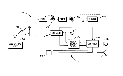
FIG. 1 is a circuit diagram illustrating a radiotelephone system.
FIG. 2 is a circuit diagram illustrating a frequency spreading circuit.
FIG. 3 is a circuit diagram illustrating a frequency spreading circuit
for the circuit of FIG. 1.
3 0 FIG. 4 illustrates signals in the circuit of FIG. 3.
Detailed Description of the Preferred Embodiments
A communication device comprises a receiver circuit receiving a
35 modulated receive signal within a first bandwidth. A reference oscillator
21 9833~
.
generates a first clock signal at a first frequency, the first clock sign-al
having harmonics. A synthesizer circuit coupled to the reference signal
generator and to the receiver is responsive to the first clock signal to
demodulate the modulated receive signal. A frequency spreading circuit
is also coupled to the reference oscillator to selectively modulate the first
clock signal with a frequency spreading signal to produce a modulated
clock signal having spread modulated harmonic frequency components.
The frequency spreading circuit selectively combines the frequency
spreading signal with the first clock signal to spread harmonics of the first
clock signal over a frequency bandwidth greater than the first bandwidth.
A control circuit is coupled to the frequency spreading circuit to receive
the modulated clock signal and operates at the frequency of the
modulated clock signal. The circuit thus selectively generates a
modulated clock signal such that the harmonic frequency signals are not
spread into multiple channels when the master clock signal harmonics
are not in the presently selected receiver channel.
A radiotelephone system 100 (FIG. 1 ) includes communication
devices 102 and 104 that communicate over a communication link 106.
The communication devices can be any two or more compatible devices
such as MODEMs (a device having both a modulator and a
demodulator), telephones, a cordless or a cellular radiotelephone, two-
way radios, a radio, a base station, a cordless telephone base, a radio
dispatch center, a radio transmission station, or the like. As used herein,
"communication device" refers to each of these and their equivalents.
The illustrated communication devices 102 and 104 exchange
information via a wireless communication link 106. However, the
communication link 106 can be a twisted wire pair, a coaxial cable, a
satellite link, or the like. Hence, "communication link" as used herein
refers to each of these and their equivalents.
The illustrated communication device 104, a radiotelephone,
includes a receiver circuit 108 including a detector 112, a transmitter 110,
and a controller 1 14. The receiver receives modulated signals from the
communication link 106 via antenna 116 and outputs signals having a
stepped down frequency to detector 112. The detector 112 demodulates
3 5 the stepped down signals to generate signals input to controller 1 14. The
21 98337
controller 114 can be implemented using a digital signal processoF, a
microprocessor such as the HC-11 available from Motorola, Inc., or the
like, and associated commercially available known circuitry.
The controller 114 responds to audio signals received from
detector 112 to generate analog signals which drive speaker 115. The
controller 114 is responsive to audio signals from microphone 117 to
- output signals to transmitter 110. Transmitter 110 generates modulated
signals from the signals output by controller 114 and the modulated
signals are input to antenna 116 for communication over communication
1 0 link 106.
The illustrated receiver circuit 108 is a double heterodyne receiver,
but alternately could be any conventional receiver circuit. The illustrated
receiver includes a filter 120, a mixer 122, a filter 124, a mixer 126 and
detector 112. A synthesizer circuit 130 is coupled to the receiver circuit
108 to provide a channel select signal to mixer 122 and an oscillating
signal to mixer 126.
A reference oscillator 132 is coupled to the synthesizer circuit 130
and to a frequency spreading circuit 134. The reference oscillator 132
generates a reference signal, or clock signal. The clock signal is input to
the synthesizer circuit 130 as a reference signal and to the frequency
spreading circuit 134 as a clock signal. The frequency spreading circuit
134 combines the clock signal with the frequency spreading signal to
generate a modulated clock signal.
The operation of the communication device 104 will now be
described with reference to the illustrated radiotelephone system 100. -
The communication link 106 in the RF wireless systems is defined by a
predetermined frequency range including a plurality of different channels
in which signals are communicated. This frequency range is passed by
the wider bandwidth filter 120. For example, the up-link channels (from a
base station to a mobile station) in the Global System for Mobil
Communications (GSM) are all within the frequency band from 925 MHz
to 960 MHz, and this frequency band is passed by filter 120. Signals
outside of the pass band of filter 120 are noise to the receiver, and are
attenuated by filter 120 to remove them from the signal input to detector
112.
- 2198337
The mixer 122 steps down the frequency of one of the charlnels
passed by filter 120 to a particular intermediate frequency associated
with filter 124. The bandwidth of filter 124 is narrower than filter 120, and
is preferably equal to the bandwidth of one channel. Filter 124 thus
5 passes only the one channel from filter 120 whose center frequency is
the center frequency of filter 124. For example, the channels in the GSM
system have center frequencies spaced at 200 KHz intervals and are
within a pass band of approximately 200 KHz. Accordingly filter 124 for
GSM has a bandwidth of approximately 200 KHz.
l O Mixer 122 selects the channel passed by filter 124 responsive to a
channel select signal from synthesizer circuit 130. Each channel in the
frequency band passed by filter 120 has a unique center frequency. The
channel select signal input to mixer 122 from synthesizer circuit 130 is an
oscillating signal which is combined with the signals from filter 120 to
reduce, or step down, the frequency of signals output by filter 120. The
amount that the signals are stepped down is determined by the frequency
of the signal from synthesizer circuit 130. By varying the frequency of the
channel select signal input to mixer 122, a different channel's center
frequency is stepped down to be passed by filter 124. It is important that
the frequency of the channel select signal be accurate so that the center
frequency of the desired channel is stepped down to the center of
frequency of filter 124 and all the information in this channel is passed to
the detector 112.
The output of the filter 124 is input to mixer 126, which combines
the filtered signal with another signal from synthesizer circuit 130. Mixer
126 steps down the intermediate frequency signal output by filter 124 to
a base band frequency at which the detector 112 operates. It is important
that mixer 126 reliably step down the information signal for detector 112
so that information is not lost by receiver circuit 108.
A reference oscillator 132 having a crystal is used to generate a
local reference signal. Synthesizer circuit 130 is connected to the
reference oscillator 132 and to controller 114. The synthesizer is
responsive to the local reference signal and a channel number from
controller 114 to generate signals for mixers 122 and 126. The frequency
spreading circuit 134 is also connected to the reference oscillator 132
21 98337
-
and to controller 114. The frequency spreading circuit 134 is- responsive
to the local reference signal to generate a clock signal for controller 114
and to selectively spread the harmonics of this clock signal. Because the
frequency spreading circuit and the synthesizer are connected to the
S same reference oscillator, both circuits can use a common crystal,
thereby reducing the number of oscillators required for communication
device 104. This achieves a cost and weight reduction for the device.
Controller 114 includes the digital circuitry within communication
device 104. Controller 114 is comprised of circuitry which operates
1 0 synchronously with master clock signals output by the frequency
spreading circuit 134.
The frequency spreading circuit 134 includes an input buffer 202
(FIG. 2), a summer 206, a switch circuit 208, and an output buffer 210.
The input buffer 202 isolates the reference signal, or clock signal, input to
synthesizer circuit 130, creating a buffered clock signal input to summer
206. The signal from input buffer 202 is illustrated connected to summer
206 through a resistor 204 which sets the level of the buffered clock
signal input to the summer. A wire alone, a filter, or the like, can be used
instead of the resistor.
The switch circuit 208 receives a frequency spreading signal from
the synthesizer circuit 130 and a bias signal from controller 114. The
bias signal turns switch circuit 208 "ON" and "OFF". When the switch
circuit is ON, the frequency spreading signal is input to the summer 206
and summed with the buffered clock signal, the resultant signal passed to
the output buffer 210. When switch circuit 208 is OFF, the buffered clock
signal alone is passed into the output buffer 210. The output buffer 210
can be implemented using a comparator, a limit circuit, a logic inverter
with its input DC biased at half its logic threshold (e.g., 2.5 volts for a 5
volt inverter), or the like.
When switch circuit 208 is ON, the output buffer 210 receives the
summation signal and outputs a signal having phase modulation
resulting from the addition of the frequency spreading signal added to the
buffered clock signal. In this manner, the buffered clock signal is
modulated by the frequency spreading signal to produce a modulated
clock signal. When the switch circuit 208 is OFF, the output buffer 210
- - 21 q8~37
will not output a substantially modulated signal as the frequency- -
spreading signal will not alter the buffered clock signal. The buffered
clock signal is thus passed through the frequency spreading circuit
without being modulated when the switch circuit 208 is OFF.
S The level of the bias signal also adjusts the modulation index bychanging the amplitude of the modulation signal. The switch circuit can
be implemented using any suitable switch such as a relay, a field effect
transistor (FET), an npn (negative-positive-negative) bipolar transistor, a
- pnp (positive-negative-positive) bipolar transistor, an optical switch
1 0 including a light emitting diode (LED) and photosensitive element, or the
like.
An embodiment of the frequency spreading circuit 134 and
synthesizer circuit 130 for a radiotelephone is illustrated in FIG. 3. The
reference oscillator 132 is provided by an oscillator circuit 302 coupled to
a crystal 304. The oscillator circuit 302 regulates the reference oscillator
output such that the local reference signal, or clock signal, at junction 305
has a fixed predetermined frequency. The reference signal is input to a
divider 350, a phase lock loop 352, and a phase lock loop 353, in
synthesizer circuit 130. The divider 350 produces the frequency
spreading signal input to the frequency spreading circuit 134 at input
312. The phase lock loop 352 generates the oscillating signal input to
mixer 126. The phase lock loop 353 generates the channel select signal
input to mixer 122.
The phase lock loop 353 includes a programmable divider 356
responsive to a channel signal from digital circuitry 342 to output a
divided down signal according to the channel to be selected. A phase
detector 360 compares the phase of the programmable divider to the
reference signal from reference oscillator 132. The phase detector
compares these signals and outputs a signal indicating the difference.
The loop filter 358 filters this signal to produce a control signal for an
oscillator 354. The oscillator frequency is set by the control input thereto
from the filter 358. This signal is fed back to the programmable divider.
The phase lock loop 353 will adjust the frequency of the controlled
oscillator until the phase difference detected by the phase detector 360 is
3 S substantially zero. The phase lock loop 352 is similar to phase lock loop
21 98337
353, except that phase lock loop 352 does not include a prograrnmable
divider receiving the channel signal.
The reference signal from oscillator circuit 302 is input to input
buffer 202, the output of which is the buffered clock signal, being a
S square wave clock signal having a fixed predetermined frequency. The
output of input buffer 202 is converted to a sinusoidal signal, A, by filter
306. Filter 306 comprises a resistor 316 and a capacitor 318. The
resistor 204 sets the level of the buffered clock signal summed at the
input of output buffer 210. If the master clock signal is a sinusoidal signal,
the capacitor 318 can be omitted.
The bias signal at output 310 of digital circuitry 342 is connected to
a resistor 320, which is connected to the collector of a transistor 322~ The
resistor is a load resistor for the amplifier circuit provided by transistor
322 and the associated components. The impedance of this resistor can
be changed to change the gain of the amplifier. By selecting the gain of
the amplifier, the amplitude of the frequency spreading modulation signal
is set. The frequency spreading signal input 312 is connected via a
series of elements, including capacitor 328 and resistor 330, to the base
of a transistor 322. The capacitor 328 removes any DC (direct current)
shift from this modulating signal. A resistor 324 is connected between the
collector and the base of transistor 322, and a resistor 326 is connected
between the base and the emitter of transistor 322. The collector of
transistor 322 is connected to a resistor 332, which is connected via a
capacitor 334 to a summing junction 308 at which point the voltages from
switch circuit 208 and lowpass filter 306 are summed. The summing
junction 308 is connected to output buffer 210 having a threshold level
Vth. When the signal at summing junction 308 is greater than the
threshold Vth, the output of output buffer 210 has a high logic level.
When the signal at summing junction 308 is less than Vth, the output of
3 0 output buffer 210 is a low logic signal. The Vth voltage level is normally
chosen such that the duty cycle of the output signal from output buffer 210
is 50%. The resulting modulated clock signal is input to digital circuitry
342 as the clock signal at which the digital circuitry operates.
In operation, and with reference to FlGs.1, 3 and 4, the buffered
clock signal output by input buffer 202 is filtered in filter 306, buffered a
2 1 98337
second time in output buffer 210, and passed to the digital cir~uitry-342
for most channels. The buffered clock signal is not modulated with the
frequency spreading signal because the bias signal has a voltage level
of 0, which prevents the switch circuit 208 from passing the frequency
5 spreading signal to the junction 308. However, for those channels that
include a harmonic of the master clock signal, switch circuit 208 is turned
ON by inputting a bias signal at output 310 that biases the transistor
circuit into an amplifier. The frequency spreading signal at input 312 is
then combined with the buffered clock signal at the input of the output
1 0 buffer 210. As shown in FIG. 4, the buffered clock signal VA has a fixed
frequency. The frequency spreading signal VB has a much lower
frequency than the buffered clock signal. For example, buffered clock
signal can be approximately 13 MHz and the frequency of the frequency
spreading signal can be approximately 500 KHz, both signals derived
15 from the reference oscillator 132. The combined signal Vc is input to
output buffer 210, having a fixed threshold Vth, when the switch circuit
208 is ON, whereas the oscillating master clock signal is input alone
when the switch circuit is OFF.
The output signal VD of the output buffer 210 is the master clock
20 signal for the digital circuitry 342. The master clock signal is a fixed
frequency signal set by the buffered clock signal and the threshold
voltage Vth when the switch circuit 208 is OFF. When the switch circuit
208 is ON, the master clock signal is a square wave signal that is a phase
modulated signal at the buffered clock signal fundamental. This
25 modulated clock signal produces wide band modulation at the harmonics
because the amount of modulation is multiplied by the harmonic number.
The average frequency of the phase modulated signal will be near the
buffered clock signal frequency. The higher harmonics of the resultant
master clock signal are spread out, such that they will not substantially
30 interfere with the received signal in a single channel. It is envisioned that the amplitude of the modulating signal and the threshold signal are
selected such that the pulse duty cycle of the resulting modulated clock
signal varies from 45 to 55 percent when the switch circuit is on. If the
duty cycle drops below 45 percent, the digital processor may have
35 difficulty following the clock signal.
- 21 ~8337
The modulation will now be described with reference to the-
waveforms VA, VB, VC, Vth and VD in FIG. 4. Waveform VA is the buffered
clock signal running at frequency fA. Waveform VB jS the frequency
spreading signal, which is a sinusoidal signal running at frequency fs.
5 Waveform Vc is the signal generated by summing VA and VB. Vth is the
cut-off amplitude of output buffer 210 (FIG. 3). Waveform VD jS the
modulated clock signal generated by passing waveform Vc through a
output buffer 210. As can be seen in FIG. 4, the variation in the amplitude
of the first clock signal VA by summation with the frequency spreading
10 signal causes a variation in phase, or phase modulation, in the
modulated clock signal.
The voltage, VA, of the first clock signal having a peak amplitude of
A volts, a frequency of fA, is described as follows as a function of time t:
1 5 VA = A * Sin{ (2~[*fA) * t }
Similarly, the voitage VB of the frequency spreading signal has a
peak amplitude of B volts and a frequency of fs, is described as follows
as a function of time t:
VB = B * Sin{ (2~*fB) * t }
- The summation signal voltage Vc is the summation of VA and VB.
The summation signal is described as follows:
VC = A * Sin~ (27~*fA) * t } + B * Sin{ (27t*fs) * t }
If there is no modulation waveform present, such that the voltage of
the frequency spreading signal VB jS zero, the output buffer 210 output
30 waveform VE jS a square wave without any phase modulation, having a
duty cycle of 50%. In this case, the comparator output amplitude D is
described as follows:
- 10 -
21 98337
VD = (.5 * D)+(2*D/7~)*~{ { 1/[(2*n)-1]} ~ Sin {[(2*n)-1]*(2*~*fA)~ }
n=l
With the frequency spreading signal having a non-zero value,
modulation can be produced. However, the suppression of the amplitude
of the harmonic must be achieved without causing too much phase
distortion of the fundamental in modulated clock signal VD. The distortion
fundamental a is the peak percentage deviation of the square wave duty
cycle. The amplitude of the frequency spreading signal VB jS selected
such that the duty cycle of the modulated clock signal VD jS within range
of 50% +/- a If f B, the frequency of the frequency spreading signal, is
significantly lower than fA, the first clock signal frequency, then VB jS
determined as follows:
VB =VA * Sin [ .5 * (a /100) * f~ ]
Typically, we need the peak percentage phase deviation, a to be less
than 5%. This gives a VsNA ratio requirement of .079 for a = 5%.
The modulated clock signal can be expressed as follows, where
Jm( ) denotes mth order the Bessel function of the first kind:
VD = (.5 * D) +(2*D/~)*~ ~ ~ { 1/[(2*n)-1] } * { Jm[n*.S*(a~100)] }
2 5 n= i m=-~
* Sin { [(2*n)- 1 ] *(2*~*fA ) +m*(2*7~*fs) } }
For a small a the amount of suppression of the nth clock harmonic is
3 0 approximately equal to 1 O*Log{Jo[n*.5*(a/100)]}. For example, if a = 5%
and n = 80, then the suppression is 1 O*Log[Jo(2)] = 6.5 dB
In a reduction to practice for GSM, the clock signal was
approximately 13 MHz and the modulation signal approximately 500
KHz. This resulted in interference with the received signals in channels 5
and 70. These channels are at 936 and 949 MHz, respectively, which
2 t 98337
are the 72nd and 73 rd harmonics of the master clock signal. -The circuit
provided approximately 7 dB improvement in desensitization, which is a
significant improvement over systems without frequency spreading.
Additionally, this improvement was achieved at a very low additional cost
5 relative to circuits without frequency spreading.
One difficulty of clock modulation techniques is spreading
harmonics into other channels can cause a good channels to become
desensitized. If this occurs, the switch circuit 208 can be provided. The
switch circuit eliminates this problem by enabling frequency spreading
10 only when the selected channel coincides with a harmonic of the master
clock. In the reduction to practice noted above, the frequency spreading
circuit is enabled by turning switch circuit 208 ON only for channels 5 and
70. If the switch circuit 208 is removed, the modulation clock signal at
input 312 can be coupled through a resistor and a capacitor to output
15 buffer 210, through a capacitor alone, or through transmission wires
capacitively or inductively coupled.
In order to reduce the current drain by the switch circuit 208, which
is desirable in battery powered devices to improve the operating time for
a battery, additional criteria can be employed to determine when the
2 0 switch circuit is turned ON. Thus, the switch circuit can be turned ON only
when the selected channel coincides with a harmonic of the master clock
and the receiver is operating near its sensitivity limit. This later condition
may be determined from the bit error rate, or as an example in a GSM
radiotelephone, from the RX_LEV or the RX_QUAL signals. The
2 5 RX_QUAL signal is generated by the radiotelephone, and has a range
from 0 to 4. RX_QUAL of: 0 is for a bit error rate between 0.0 and 0.2%; 1
is for a bit error rate between 0.2 and 0.4 %; 2 is for a bit error rate
between 0.4 and 0.8%; 3 is for a bit error rate between 0.8 and 1.6%; and
4 is for a bit error rate between 1.6 and 3.2 %. The RX_LEV ranges form 0
30 to 100 and corresponds to the power of the receive signal including
interference. The range of 0 to 100 corresponds to an input level of -110
to - 10 dB. One criteria that can be used is that the frequency spreading
circuit 134 is only used to modulate the buffered clock signal when
RX_QUAL signal is greater than 1 and the selected channel is a
35 harmonic of the first clock signal. Another criteria that can be used is that
~1 98337
-
the frequency spreading circuit is only used to modulate the buffered
clock signal when RX_QUAL is weak, such as below 15 for example, and
the selected channel includes a harmonic of the buffered clock signal. ,'n
this manner, the switch circuit is only turned ON when the improvement in
S the signal level is necessary, thereby reducing the current drain by the
switch circuit 208.
Thus it can be seen that a circuit is disclosed that provides
effective frequency spreading. The circuit provides clock harmonic
spreading in a circuit that is readily implemented using few circuit
10 elements and at a lower cost than circuits heretofore utilized.
Additionally, by selectively modulating the clock signal only in those
channels that include a harmonic of the master clock signal, it is possible
to avoid desense of good channels by frequency spreading.