Note: Descriptions are shown in the official language in which they were submitted.
WO 96/07187 2 1 9 8 4 8 8 PCT/US95110S58
PRlNTEiD ClRCUlT BOARD I1~I1)U~ 1
Tecbnic~ Field
This invention relates in general to electronic ~RR~mhli~R, and
6 more Rperifi~ y to an inductor formed on a printed circuit board.
~ r ~, I
Electronic circuit designers muEt constantly address the issue of
interference such as radio frequency hlLelr~,~,.ce (RFI) and
ID clccL~ ti~ interference (EMI) which affect the p~rf~rm~nre of the
circuits which they design. Typical solutions to in~ lC~: problems
include separating circuits from one another in order to minimize
i..i~lre~ .ce, placing metal "cans" over sensitive circuits or circuits
which are the generators of hlle,re~ ce signals (e.g., oscillator circuits,
16 etc.). Another problem p.~:s~..t~d when designing electronic circuits
such as radio circuits is minimi7ine the amount of board space required
to impl~m~nt. a given circuit. Furthermore, in the case of some circuits
such as filters and transmitter circuits, it is also i...pull~lt to design
circuits which can be tuned or adjusted in order to overcome the changes
20 in circuit~ due to component tolerance variations, etc.
Cost is also a r,nn~ l :n.,. An inductor which is built into the
same printed circuit board as the rest of the circuitry reduces material
does not add much ~ lit.inn~l cost to the m~nllf~lrt~lrine cost of the
electronic assembly. Another issue cullrrullit:d by designers is
2~ ~ ... r ~ ,. L tolerances. Inductor make tolerance is a factor which
inflllenrPR circuit design and ~nm~tim~R leads to high cost, tight
tolerance inductors. A printed circuit board inductor of the type
described in the present invention can be culls~Lru~d ine~pensively into a
printed circuit board, using ~ ",R and spacing that conform to the
~0 circuit board m~nllf~rtllrers process limit~tinnR and hold tighter make
tollor~nres than their discrete counterparts. Furthermore, there is a
need in the art for an inductor which can be tunable and which can
provide for improved shielding against illt~rrt~ ce.
36 Brie~1~ Drawmgs
FIG. 1 is a side view of a multilayer circuit board in accordance
with the invention.
2t ~8488
WO 96/07187 2 PCT/US95/105.'i8 ~
FIG. 2 i8 an exploded view of some of the intsrmerlisltr layers of the
multilayer circuit board shown in FIG. 1.
FIG. 3 shows a tunable planar inductor having inrlllctonre
adjustment means in accordance with the invention.
FIG. 4 shows a tunable planar inductor having an electronically
adjustable inrlnrtonr.o in accordance with the invention.
FIG. 5 shows an exploded view of similar intr rm~ te layers as
shown in FIG. 2, in this case using standard board construction
techniques.
FIG. 6 shows another ,omhorlimr~nt in which a printed circuit
board inductor is shielded by a ground plane and a shield in a~,l.l UlC6
with the invention.
FIG. 7-9 show different printed circuit board inductors in
accordance with the invention.
De~iled n~ _ .. i~d -~ ~f he P~ r
While the ~ , iri. . L.. ", concludes with claims defining the
features of the invention that are regarded as novel, it is believed that the
invention will be better nn(lPrefood from a cnn~itlPr~tinn of the following
20 description in con,iunction with the drawing figures.
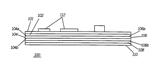
Referring to FIG. 1, there is shown a pop~ tPd multilayer printed
circuit board 100 having a printed circuit board inductor in accordance
with the present invention. Multilayer circuit board 100 as shown
includes 6 layers 101, 102, 104, 106, 108 and 110. Preferably, the circuit
25 board layers are formed from a glass l~h~olced epoxy such as FR4, or
other materials used to form printed circuit boards. The top surface of
multilayer circuit board 100 is pop~ t~d with a plurality of electronic
rompnn~nt~ 112 as is well known in the art. Although FIG. 1 is shown
as a SiY layer multilayer board different number of layers can be
90 designed for ~Ir~p~snrling on the particular design re~lui~ L~.
In FIG. 2, an eYploded view of some of the i.~ e~ Iayers 104,
106 and 108 of multilayer circuit board 100 are shown. In accordance
with the invention, a printed circuit inductor 200 is formed on layer 106.
Inductor 200 is formed by interrnnnPrting mAf~lli7~tinn patterns 216
35 located on first surface 106a with m.otslli7~tion patterns 218 located on
second surface 106B using interrnnmsctic)n vias 214. The vias could be
blind or buried, as would be the case for a sequentially i~min~ted circuit
board, or the vias could penetrate each layer of the circuit board as will be
2 t 98488
WO 96/07187 3 PCIIUS95/105~8
discussed in reference to FIG. 5. Inductor 200 as shown forms a multi-
turn inductor having first 212 and second 206 tPtminolc. In &cculd~ce
with one Pmho~imPnt of the present invention, the inductor 200 is
shielded against external i~lelr~ e by ground planes 202 and 204
5 which are located so as to be in olignmPnt or rPgictrot;~n with inductor
200 when layers 104, 106 and 108 are mated together. When layers 101-
110 are lo".;"~ d together to form the multilayer board, ground planes
202 and 204 8 -hc+ontiolly overlay inductor 200, thereby providing
interference protection to the inductor.
Ground plane 202 i9 formed by a mPtolli~oti~)n pattern located on
first or top surface 104A of layer 104. Ground plane 204 is formed on the
bottom or second surface 108B of layer 108. M~tolli7Otir~n patterns 202
and 204 are ~lpctrirolly coupled to the multilayer circuit's ground
potential using conventional runners (traces) and via interc~nnPrtir~n
15 tPrhniqllPc. In order to hlLe~ n~l inductor 200 with other electronic
r~lmponPntC. 112 located on multilayer board 100 one or both terminals 212
and 206 are interc-~nnPrted to other layers of circuit board 100 using
mPtolli7pd vias. For example, terminal 212 can be electrically coupled to
one of the upper layers 101 or 102 of circuit board 100 by providing a
20 mPtolli7Pd via 210 in order to hlk ~ u.~nP~ l via 212 through layer 104 and
up to a p,~,l..l ,..; IlPd point on layer 101 or 102. In order to avoid short
circuiting via 210 to ground plane 202, a non-mPtolli7Pd area 208 is
provided between via 210 and ground plane 202. Pl t r~,bly, the
illt.é~ P~ .. vias 210 used to interconnect the inductor 200 located in
25 the; "~ l e layers of circuit board 100 are kept as short as possible
in order to minimize effecting the in~lnrton~-e value of inductor 200 as
well as prevent in~ f~.ell. e signals from effecting the circuit.
Although ground planes 202 and 204 reduce the in~ r+onr~ value
of inductor 200 slightly, this change in intlllrtonrP due to the shield can
30 be ~ mrpngot~d for by adjusting the ~ "g of inductor 200. For
example, the mPtalli70ti~ n runners 216, 218 can be decreased in width,
the size of vias 214 can be decreased in size, more turn(s) can be added to
the inductor, etc. Ground planes 202 although shown as not taking up
the entire surface of the int.ormPrli~te layers they reside on, could take
35 sllhQ+ontiolly the entire surface of their co..~ ...tling layers if needed to improve ghiPIrling
The overall area taken up to form inductor 200 is dictated by the
required in-lnrtonrP the amount of current that the inductor will carry,
WO 96/07187 2 1 9 8 4 8 8 PCI/US9~/10558
the required Q (quality factor) of the inductor, and the minimnm feature
size available from the PCB vendor. A typical four turn coil would
require an area of approYimately 2.413 millim~t~r by 1.016 millimeter
using conventional printed circuit m~nnf~rtllring techniques, although
5 smaller footprint~ can be achieved using more expensive printed circuit
board m~nllf~rtllring techniques.
In order to save m r In, rU. ~ ~ I hlg costs, instead of using blind vias
as shown in FIG. 2 which cost more to m~nllf~rtllre, standard board
construction can be used to m~nllf~rt~.lre the multilayer circuit board as
10 shown in FIG. 5 in order to savej ~sts. In FIG. 5, all the vias 508 shown
go through all the layers of the _ultilayer circuit board including the
intPrm~i~t-~ layers 502, 504 and 506. In the case of ground plane layers
502 and 504, the vias are electrically isolated from the ground planes 510
and 512 by areas which surround each via 508 which are not platted.
15 Ground plane 510 is located on the top surface of layer 502, while ground
plane 512 is located on the bottom surface of layer 506 in order to isolate
the ground planes from the traces 516.
Although the inductor 200 shown in FIG. 2 has been shown as an
equivalent of air wound coil having the printed circuit board as the
20 dielectric, other forms of printed circuit inductors can work with the
present invention. Such as, inductors which are formed on one surface of
the printed circuit board using no vias, other inductors which use two or
more major surfaces of substrates to form, inductors which are straight
lines or have other shapes, etc. In FIGs 7-9 some other different printed
26 circuit board inductors which can be used with the present invention are
shown. FIG. 7 shows a straight line inductor having traces 702 on top
surface and trace portions 704 on the bottom surface which are
interr~nn~rt~l by vias 706. In FIG. 8, a single surface winding inductor
which is formed by trace sections 802 which are interrnnn~ct~l by serial
30 rf~nn~rting vias 804 is shown. In FIG. 9, a dual surface inductor is
shown having section 902 on the top surface and trace sections 904 on the
bottom surface. Other types of inductor shapes and designs other than
those shown can also be utilized.
When ml~mlf~rtllrinE electronic circuit boards, such as radio
35 frequency circuits, it is c~metim~ required to tune the circuits during
the mU".,ru. ~ ...g process. This is typically caused by rr)Trlronpnt
tolerance differences found between circuit boards due to variations
between electronic r~mrrmlqnt~ In FIG. 3, a tunable printed circuit
WO 96/07187 5 2 1 9 8 4 8 8 PcT~usgsll0ss8
inductor 300 in accordance with another PmhotlimAnt of the invention is
shown. Inductor 300 includes a plurality of inter~onnPcti~n vias 306
which elPctr~ y interconnect top runners 308 with bottom runners 310.
Inductor 300 includes two end terminals 302 and 304. In this
5 PmhorlimPnt, inductor 300 includes one or more intlnt-toncP adjustment
means which can take the form of met~ pd runners or trimms~hlP
resistors 316 and 318. Tnrlnrt~nr~ adjustment runners 316 and 318 are
met~llis!Pd runners which short some of the turn~ of inductor 300. In
order to increase the in~ f~n~A value of inductor 300, one or more of the
10 adjustment runners 316 are cut using well known laser trimming
equipment or by simply merh~nirfilly cutting one or both runners 316,
318. Instead of mPtolli7Pd runners, laser trimm~hlA resistors as known
in the art having ~ vlJl;c~te resistance values can be used, and
trimmed in order to adjust the inrlnctonre value of inductor 200.
As shown in FIG. 3, with both intlllrtonce adjustment runners in
place, inductor 300 forms a 2 1/2 turn coil with its terminals being 302
and 312. If runner 316 is cut, the inductor becomes a 3 1/2 turn coil with
its terminals being 302 and 314. Finally, if both of the in~urton~e
adjustment runners 316 and 318 are cut, the inductor becomes a 4 1/2
20 turn coil, with terminals 302 and 304. Inductor 300 could be used for
example, in a radio trAn~mitt~r circuit wherein the power output of the
trSlncmit+Pr could be adjusted during m~nnf~t.lre by trimming one or
more of the in~lnct~nce ad, u~LI. ~i runners. If the vias 312, 314, and 304
where spaced ~lv~ L~:ly, the runners 316 and 318 could be replaced
25 with resistors, or zero ohm jumpers if desired, to decrease the
intlllctDnre again.
FIG. 4 shows a tunable inductor or coil 400 having an
electronically adjustable in-lllrt~nre value in accordance with the
invention. Instead of using mPt~lli7Pd runners 316 and 318 as shown in
30 FIG. 3 in order to adjust the imlll~t~n~ e value, in FIG. 4, a transistor 408such as a field-effect transistor (FET), bipolar junction transistor (B~TT)
or other type of appropriate L~ ;DLvl as known in the art is used to
~nt~m~ti~ lly switch the in~ t~n~e value of inductor 400. Transistor
408 is located between two adjacent turns of the printed circuit inductor
35 400. Transistor 408 is either in a first state where vias 406 and 404 are
shorted together or in a second state where the L~ Lvl is open and
there is no direct ~ . between vias 406 and 404. In the first state
WO 96/07187 2 1 q 8 4 8 8 ~ rJ -51 - ~
inductor 400 acts as a 3 L~'2 turn coil, while when ~L~lllbib~UL 408 is in the
second state coil 400 acts as a 4 1/2 turn coil.
Tran~istor 408 i8 switched from the first state to the second state by
a cvntrol signal sent via line 410. The control signal can be gPnPr~ted by
5 a number of cvnventional hardware circuits such as a mi~ lV~bbU~ or
other type of hardware circuit. Electronically tunable cvil 400 prvvides the
ability of adjusting the intlnrt~nrP value of inductor 400 even when
inductor 400 is formed within intermPrli~tP layers of a multilayer circuit
board as shown in FIG. 1. This provides the opportunity of having an
10 inductor located within a multilayer circuit board as dibscussed v~ith
reference to FIG. 1 and still be able to adjust its in~lllrt~nrp value.
Electronically tunable inductor 400 can be used for many electronic
circuits were a tunable inductor is required. For example, in radio
transmitter circuits in order to adjust the power output level, etc.
In FIG. 6, another PmhotlimPnt of the present invention in which a
printed circuit board inductor 602 is shielded by a ground plane 608 and a
shield 610 is shown. In this Pmho~limPnt a printed circuit board
inductor is formed on substrate 604 similar to that shown in FIG. 2. A
second substrate 606 having a ground plane 608 etched on the bottom
2v layer is attached to the first substrate 604. And a shield such as a metal
can 610 is attached to the top layer of substrate 604 in order to fully shield
inductor 602 from hlteLr,-l-,dllce. Inductor 602 can include the in~lnrtSInrP
tuning means previously discussed if tuning is a requirement.
In summary, the present invention provides for a shielded planar
25 inductor which can be used in ~-. viru .,enlb were a shielded inductor is
required, such as in radio frequency circuit ~i~plir~tinnR By locating the
inductor within the hlLr-~ luer~ e layers of a multi-layer circuit board,
board space on the top surface of the multi-layer circuit board i8
cvnserved for other electronic rnmpnn~ntR In another aspect of the
~0 present invention, a planer printed circuit board inductor 300 or 400
includes an in~nrt~nre tuning means such as mptsllli7pd runners 316,
318, an electronic switching device 408, or other means in order to adjust
the inrlnrt~nrP value. The electronically tunable inductor shown in FIG.
4 can also be formed within intPrmP~ tP layers of a multilayer circuit
35 board in order to conserve board space and also to allow the inductor to be
shielded if required.
What is claimed is: