Note: Descriptions are shown in the official language in which they were submitted.
21 98491
~ w 096/07116 ' r~l~k~ ~r~4s
A METHOD OF MAKING AN OPTICAL WAVEGUIDE
TO FIBER CONVECTOR USING A FREE-STANDING
FLEXIBLE WAVEGUIDE SHEET
The invention pertains to a method of making an optical device
comprising a substrate on which are integrated a layered optical
waveguide component comprising a polymeric guiding layer sandwiched
between two deflection layers of a lower refractive index than the
guiding layer, and optical fibre ends, the optical fibre ends being
positioned in grooves.
Optical fibre ends attached to the integrated optic device are usually
referred to as "pigtails," and the process of providing a waveguide
component with such pigtails is referred to as "pigtailing." The
invention also pertains to the pigtailed optical waveguide devices so
obtainable and to the free-standing, flexible waveguide sheets used in
making them.
In general, flexible waveguides are known. E.g., JP 04/Z32906
discloses a flexible multilayer light guiding sheet suitable for use
in signal transmission, e.g., with light splitting such as optical
data linking for cars.
JP 05/281428 pertains to a flexible optical inte,~u""~c~ion board
comprising a flexible optical waveguide mounted onto a base plate that
can have various shapes (e.g. curved).
From JP 04/274402 it is known to provide a flexible waveguide by
coating a polyamic acid solution onto a substrate, irradiating it so
as to produce a precured film, removing said film from the substrate,
and curing it so as to form a polyimide waveguide. A polyimide film
having a lower index of refraction than the polyimide waveguide film
is used to coat at least part of an upper layer and a lower layer of
the waveguide film.
WO 96107116 ~ /r.l .. 45
2 1 98491
It is known to produce polymeric flexible waveguides having a
refractive index pattern, see JP 52/138 146 which teaches forming a
polymeric film, diffusing a monomer in it, and polymerizing the
monomer in selected areas. Comparable techniques have been disclosed
in JP 78/026813 and JP 54/088144.
From U5 4,496,215 it is known to provide an optical intel.u"".~Lion
device comprising straight and curved segments, in which the optical
inte cu" ~Lion is in the form of fibres (laid in a layered flexible
structure).
These references do not specifically address the problem of pigtailing
polymeric optical waveguide components. This continues to be one of
the principal challenges when making optical waveguide devices. Making
a proper connection with a minimum loss of light (coupling loss)
between the guiding layer of the waveguide component and the core of
the optical fibre is a cumbersome, and generally expenslve process
step. This especially holds for coupling with single mode optical
fibres.
It is known to make use of substrates (usually of silicon) having V-
shaped grooves in which fibre ends can be placed. The V-shape of the
grooves allows the fibres to be properly aligned vertically (i.e., in
respect of the height of the guiding layer) as well as laterally
(i.e., in respect of the width of waveguiding channels made in the
guiding layer). After the fibres have been placed in the V-grooves
they are usually fixed using glue, solder, or the like.
A method as indicated above, employing such a V-grooved substrate, is
known from GB 2 000 877. The method disclosed bonding the end-portions
of a plurality of optical fibres to V-shaped grooves provided on a
transparent substrate by an adhesive; casting a polymer solution onto
the fixed optical lead fibres-containing substrate, and evaporating
... ... . . _ . . _ . .. . . ..
2 1 9849 1
~ WO 96/071 16 . ~_ ll~ 7_, . 't745
the solvent. Thus, the optical lead fibres are embedded in a polymer
layer. Said polymer layer, which serves as the guiding layer of the
optical waveguide component, contains, int.al., a photopolymerizable
monomer. By selectively activating this monomer, the refractive index
of the guiding layer can be selectively decreased. Thus, waveguide
channels can be formed in the guiding layer by irradiating the
surrounding material. These channels can be made to be aligned with
the positions of the embedded ends of the optical fibres. On the
guiding layer a low refractive index coating is applied as a top
deflection layer. The substrate serves as the lower deflection layer.
The method disclosed in GB 2 000 877 has several drawbacks. In part,
these are associated with the use of the substrate as the lower
deflection layer. One disadvantage thereof is that the disclosed
method cannot be applied to make electro-optically active waveguides.
E/O-active, or NLO materials, are known. In such materials non-linear
charge polarization occurs under the influence of an external electric
field. Non-linear electric polarization may give rise to several
optically non-linear phenomena such as frequency doubling and Pockels
effect. Obtaining the desired NLO effect in polymeric materials
macroscopically requires that first the groups present in such a
material, mostly hyperpolarizable side groups, be aligned (poled).
Such poling is usually effected by exposing the polymeric material to
electric (dc) voltage, the so-called poling field, with such heating
as will render the polymeric chains sufficiently mobile for
orientation. Hence, if a polable e/o material is used in the guiding
layer, it is a requirement for poling to occur that the guiding layer
can be exposed to an electric field. To this end, two electrodes are
needed, one of which is usually applied on top of the layered
waveguiding structure, while the other is usually applied at the
bottom, i.e., in between the substrate and the lower deflection layer.
Providing such a bottom electrode is not envisaged in the method of
GB 2 OOO 877.
wos6/07ll6 2 1 9 8 4 9 1 ~ ~ I ,~. ,4~ -
Another disadvantage of using the V-grooved substrate as the lower
deflection layer is that the refractive index of such a lower
deflection layer cannot be tailored to that of the guiding layer and
the top deflection layer. Since the difference in refractive indices
(the refractive index contrast) of the layers determines the
efficiency with which light from an optical fibre can be coupled into
the waveguide and viceversa, it is a serious design limitation if the
refractive index of any one of the layers cannot be freely chosen.
This particularly holds for the deflection layers, since, depending on
the nature of the device, the requirements applicable to the guiding
layer polymer frequently are more stringent than those applicable to
the cladding layers. E.g., in the case of electro-optically active
guiding layers, the choice of the guiding layer polymer will be
determined more by its e/o coefficient than by other properties such
as refractive index. Or, if it is desired to form channels in the
guiding layer by means of "bleaching" (a photophysical change of
refractive index such as disclosed in EP 358 476), the guiding layer
polymer may be chosen for its bleaching capacity more than anything
else.
The method of GB 2 000 877 cannot be simply replaced by a method in
which a separate lower deflection layer is applied on the substrate.
To begin with, this would undo the very fibre-waveguide alignment as
taught in the disclosure. Further, if the lower deflection layer is
z5 polymeric, which is highly desirable in respect of tailoring the
refractive index and compatibility with the polymeric guiding layer,
the problem applies that the V-grooves will fill up with the
deflection layer polymer, leading either to the fibre cores being
severely misaligned with the light guiding channels of the polymeric
waveguide or unflatness and thickness nonuniformity for the waveguide
structure, or both.
~ w o 96/07116 2 1 9 8 4 9 1 P~ 1245
~ Another known method for connecting optical fibres with waveguide
devices employing V-grooved Si is known from IEEE Transactions on
C~ .ne,.Ls, Hybrids, and Manufacturing Technoloav, Vol.13(4), 1990,
pages 780-786. The method involves bonding a first substrate, a
portion of which carries optical fibres in V-grooves, with a second
substrate carrying an integrated optical circuit, the fibres and the
circuit eventually being positioned adjacent to each other. The two
substrates face away from one another, and the bonding is achieved by
means of solder bumps. This so-called flip-chip solder bump bonding is
a self aligning process, the alignment being achieved through the
action of surface tension forces during solder reflow. This method has
several drawbacks in respect of pigtailing polymeric waveguide
components. The required melting and flowing of solder generally
requires temperatures that are too high to be used with polymers. A
typical t ~Lul~ being 200~C, this will be above the glass
transition of many types of electro-optically active polymers, which
will lead to these polymers losing their activity. Further, the flux
(organic acid that prevents oxidation of the solder) that as a rule is
dispensed on the solder during reflow, is likely to attack the
polymer. Further the method has the drawback of the final product
comprising no less than three different substrates: the two substrates
mentioned, i.e., one carrying the integrated optical circuit and the
other carrying the fibres in Y-grooves, together need be supported by
a third substrate, a so-called motherboard.
The invention now seeks to provide a pigtailing method that can be
used with passive as well as thermo-optically and electro-optlcally
active waveguides, allows refractive index tailoring, and can be used
with polymers. In providing such a method, it is an object of the
invention to avoid the complicated use of three different substrates
and to wind up with a device comprising a single substrate. To this
end, the invention consists in that in a method as described in the
opening paragraph, a substrate comprising grooves, notably V-shaped
WO 96/07116 2 1 9 8 4 9 1 r. ~ . 45
grooves, is provided with a separately made polymeric structure
comprising one or more layers, hereinafter referred to as a free-
standing sheet.
The free-standing sheet can either be a single layer, or it can be a
layered structure comprising the guiding layer and at least one
deflection layer, said layered structure being applied with the
deflection layer facing the substrate. Preferably, the free-standing
sheet is a complete layered waveguide structure comprising the guiding
layer and two deflection layers enclosing the guiding layer.
In the case of the free-standing sheet being a single layer, it serves
to planarize the V-grooved substrate. After this layer has been
applied, other layers can be applied onto it, by means of spincoating,
evaporation etc. The spincoating process, which is generally
recognized to be the most convenient method for applying thin layers,
such as in the case of polymeric optical waveguides, as a rule
involves rapidly rotating the -entire substrate to be coated. Hence,
the further application of layers will necessarily involve covering
the entire grooved substrate. The planarizing layer (which may serve
as the lower deflection layer or may be an additional layer) is
therefore applied over the entire grooved surface. After the other
layers of the layered waveguide structure have been applied, a portion
thereof will have to be removed (including the co" e,~u,.ding portion
of the planarizing layer) so as to uncover the grûoves. Such removal
wlll generally have to be done by means of etching (e.g. ~2 reactive
ion etching). The use of a single planarizing layer has as its main
advantage that a polymeric layered waveguide structure can be applied
onto a grooved substrate without the grooves filling up with polymer.
Since the further spincoating steps are conventional, and allow the
formation of a well-defined layered waveguide structure, proper
alignment of fibres and waveguide may be attained. However, employing
a free-standing sheet in the form of a complete layered waveguide
~ W096107116 - IA
2 1 9 8 4 9 1 r~ 4s
structure has important additional advantages. This embodiment is less
complicated, the waste of material is reduced to a minimum, and a
smoother waveguide facet can be made. In all its embodiments, the
invention allows obtaining an accurate connection of the waveguide
with the optical fibres by adapting the layer thicknesses of the
layered waveguide structure (and, if used, the planarizing layer) to
the dimensions of the optical fibres (notably: core diameter). Thus,
the cores of the optical fibres (usually cylindrical or elliptical)
can be positioned face to face with the guiding layer of the layered
waveguide structure.
The method of the invention involves separately providing a grooved
substrate already containing fibre ends or not, and making a free-
standing sheet.
The manner in which the grooved substrate is provided is not in itself
part of the present invention. Instead, such substrates are
commercially available or can be made by methods known to the man
skilled in the art.
In principle, the substrate can be made of any material suitable for
supporting a polymeric waveguide structure. Examples are thermoset
polymers, in which the desired grooves can be made, e.g., by shaping
techniques such as injection moulding, glass, or other inorganic
materials such as silicon or GaAs and the like. In the latter
materials, grooves can be made by etching techniques known from the
semiconductor industry. In this respect silicon is particularly
preferred. The grooves preferably are V-shaped, thus providing two
facets in respect of which optical fibres can be very well kept in
place, thus allowing positioning in respect of waveguide facets most
accurately. The depth of the grooves logically depends on the diameter
of the optical fibres employed.
W O96/07116 2 1 9 8 4 9 1 P~~ nt~4S
If use is made of single mode fibres, which have a core diameter of
about 9 ~m, the substrate preferably is a monocrystalline material
exhibiting an anisotropic etching characteristic, since high accuracy
in the dimensions of the V-grooves which will contain the fibres
having a diameter of the order of 125 micron must be obtained. In this
respect silicon, gallium arsenide and indium phosphide are examples of
suitable substrate materials.
If the free-standing sheet is not a mere planarizing layer, the
grooved substrate can be provided with fibre ends before the free-
standing sheet is applied. It is preferred to provide the fibre ends
afterwards. In the case of an electro-optically active waveguide being
formed, a bottom electrode in the form of a thin layer of metal is
applied first, at least at the portion of the substrate that is to be
covered with the free-standing sheet. This bottom metallization,
preferably gold, is usually applied by evaporation or sputtering.
Particularly in this . bc'i ,L. it is preferred if the substrate
comprises tuo portions: a portion containing grooves (in which
eventually the fibres will be laid) and a flat portion, on which first
the metal layer and next the free-standing sheet is applied.
The free-standing sheet is prepared separately. In view of the
required accuracy and thickness uniformity of the layers, or single
layer, it is generally necessary to first make the free-standing sheet
on a substrate. Such a substrate will be planar (flat), so that a
layer, or layered structure, having clearly defined layer thicknesses
can be made. After the layer or the layered structure has been lifted
off the original substrate, it can be placed on the grooved substrate.
The original substrate can be made of the above-mentioned substrate
materials, silicon being preferred.
The polymeric materials from which the free-standing sheet, and
eventually the layered waveguide are built up are not crucial to the
present invention.
~ W 096/07116 r~ 4s
2 t 9849 1
The deflection layers, as well as the guiding layer in the case of a
passive optical component, can be made of any suitable polymer which
t is transparent to the wavelength employed and displays minimal optical
losses for the desired wavelength. The most important wavelength
ranges in actual practice are approx. 670 nm, from about 800 to about
1000 nm, approx. 1300 nm, and approx. 1500 nm. These last two
wavelength ranges are especially suited for use in telecommunications.
Of course, it is imperative that the guiding layer have a higher index
of refraction than the deflection-layers. The man skilled in the art
will be aware of optical polymers that can be tuned to have the
desired refractive index. Examples of suitable deflection (cladding)
layer materials are acrylate-styrene copolymers, such as copolymers of
l,yd,oxy~ll,yl methacrylate and styrene, and the same in conjunction
with maleic anhydride. It may be advantageous to apply these polymers
in the form of a prepolymer having functional end groups, and to
include a polyfunctional cross-linking agent for these end groups
(e.g. hydroxyl end groups to be cross-linked with Desmodur-N
triisocyanate). The suitable polymeric materials for passive
waveguides are known to the skilled person. Further, it is of
importance for the core and deflection layers to be easy to treat and
so processable as to give the flattest and purest possible contact
surfaces between the core and deflection layers as well as sufficient
adhesion between the core and deflection layers. The skilled person
will know which materials to select to this end. Preferably, use is
made of materials in which waveguide channels can be made by means of
irradiation, as described below.
As indicated before, in electro-optically active waveguides use is
made of polymers having a non-linear optical activity macroscopically
effected therein by means of alignment. Suitable NL0-active materials
(NL0 polymers) have been described in EP 358 476 and in, e.g.,
EP 350 112, EP 350 113, EP 359 648, US 4,867,540, US 4,795,664, and W0
91/03001. For that matter, these materials are also suitable for use
in passive wavegu.des.
WO 96/07116 2 1 9 8 4 9 1 P~ . . 45
Making the free-standing sheet in the form of a layered waveguide
structure will generally involve the following steps:
- Providing a flat substrate with a layer that is releasable upon
proper treatment, e.g., a gold layer, or a layer of water-soluble
material such as polyvinyl alcohol or water-soluble salt;
- Applying the first deflection layer polymer on the releasable
layer;
- Applying the guiding layer polymer on the first deflection layer;
- Applying the second deflection layer polymer on the guiding layer;
- Releasing the layered structure from the flat substrate by
suitably treating the releasable layer; in the case of a gold
layer such treatment will involve subjection to warm KOH (appr. 50
~C.)
In the case of the free-standing sheet comprising less than a full
layered waveguide structure, the appropriate steps can be omitted. If
the free-standing sheet is a separate planarizing that does not serve
as the first deflection layer, the layer applied on the releasable
layer can basically be any polymeric layer.
According to a particularly advantageous embodiment of the invention,
the releasable layer comprises a water-soluble material such as a salt
such as NaCl or polyvinyl alcohol. This means that agressive treatment
such as subjection to warm KOH can be avoided, and the waveguide sheet
can be released from the original substrate by dipping the entire
structure in water. It is then ready to be placed on the grooved
substrate.
In some cases, particularly when the waveguide structure is so
flexible as to give handling problems, an alternative to first
releasing the waveguide sheet and then placing it on the grooved
substrate is to perform these acts simultaneously. This can be done by
placing the grooved substrate on top of the releasable waveguide
~ WO 96/07116 2 1 9 8 4 9 1 ~ 45
structure still on the original substrate, and then activating the
releasable layer. The grooved side of the substrate has to face the
deflection layer. The original top deflection layer thus becomes the
bottom deflection layer on the grooved substrate. Although this has
been found to work without further measures, it may be advantageous to
enhance the adhesion of the waveguide structure to the grooved
substrate placed on top of it by first providing the grooved substrate
with a thin adhesive layer. This can most conveniently be a layer of
about 0.5 ym thickness of the same polymeric material as the
deflection layer. Such a thin layer also covers the bottom of the
grooves, but does not fill them up. Hence, the above-identified
drawback that occurs when a full cladding layer ~having a thickness of
the order of 3-15 ym) is applied on the grooved substrate does not
occur. Preferably, the adhesive layer is a still curable prepolymer,
which is cured (by applying heat) after the structure has been
released from the original substrate. In respect of thicknesses, it
may be mentioned that the three-layered waveguide sheet will generally
have a thickness of from about 5 to about 50 ym.
An advantage of first making a clearly defined structure of a
polymeric guiding layer sandwiched in between two polymeric cladding
layers is that the placing of the structure on the grooved substrate
does not require high accuracy. For, thi 5 waveguide sheet can be
applied on the grooved substrate with relatively low precision, and
may cover an area extending beyond that on which the waveguide
component eventually is desired. After the waveguide sheet has been so
applied, and the channels are defined and a smooth facet is etched at
the side at which the optical fibres will be positioned. All
protruding parts can be removed using any appropriate etching
technique, e.g., those known from the production of integrated
circuits (ICs). Applicable in this case are wet-chemical etching
techniques, e.g., with use being made of organic solvents or strong
bases. However, preference is given to dry etching techniques, such
w 096/07116 2 1 9 ~ 4 9 1 P~~ 4s
12
as sputter etching, reactive ion etching, or reactive plasma etching.
Such techniques are known to the skilled person and require no further
elucidation here. Alternatively, there may be etching using a laser,
mechanical etching such as grinding, cutting, drilling, or etching
through bombardment with sanding particles such as alumina, silica,
and, more particularly, pumice. The skilled person is expected to be
able to select an appropriate etchant without undue ~p~lil Lation.
Preferably, use is made of reactive ion etching (RIE) or a combination
of RIE and reactive plasma etching, while so-called laser ablation is
another very suitable technique. To make the facet, and to remove the
protruding portlons of the layered polymeric structure, a mask is
applied to cover those parts which should remain free from attack by
the etchant. These masks, the chief prerequisite of which is that they
be resistant to the action of the etchant, are known, int. al., from
IC technology. Such a mask may be preformed and made up of, e.g..
metal or synthetic material; alternatively, it can be made by applying
a photosensitive resin (photoresist) and suhs~; Lly exposing and
developing said resin in accordance with the desired pattern.
If an air gap between the optical fibres and the waveguide cannot be
avoided simply by accurate positioning of the fibres and the
waveguide, a filler, preferably low viscous, may be used to fill the
gap. In this way, providing the optical properties of the filler do
not differ markedly from those of the polymer, an inconvenient
refractive index contrast in relation to an air gap may be avoided.
Preferably the filler selected has the same, or virtually the same,
refractive index as the core layer of the polymeric waveguide. Thus
the polymer itself can very well be used as a filler, either in the
form of a solution or (in the case of a thermoset) in the uncured
state. Alternatively, use may be made of oligomers analogous to the
polymer, a glue, or some other adhesive. Suitable adhesives are for
instance the glues of the well-known epoxy or cyanoacrylate types.
~ wo 96/07ll6 . 2 1 9 8 4 9 1 r~ 24s
In the case of an electro-optically active waveguide being prepared,
the preferred method of the invention involves applying a first
electrode in the form of a metal layer (preferably gold) on the salt
layer, applying the first deflection layer, the guiding layer, and the
second deflection layer, and then applying a second electrode in the
form of a metal layer on the second deflection layer. ~ow the
waveguide structure can be poled before it is released, by applying a
suitable voltage to the two electrodes. Thereafter, the poled layered
waveguide structure is released from the flat substrate, and applied
on a guest substrate.
Usually, it will be necessary to define waveguide channels (i.e.,
lateral wave confinements) in the guiding layer. Methods of achieving
this are known. For instance, such patterns may be provided by
removing portions of the layered waveguide structure, e.g., by means
of wet-chemical or dry etching techniques, and filling the formed
voids with a material having a lower index of refraction (thus forming
a wave confinement in the form of a channel made up of material
enclosed on all sides by deflection layer material).
Alternatively, it is possible to use photosensitive material, which
can be developed after irradiation; for instance, a negative
photoresist, that is to say, material which is resistant to a
partlcular solvent (developer) after being irradiated. The developer
in that case may be used to remove non-irradiated material. However,
it is preferred to employ a positive photoresist and have the
developer remove the portion that has been irradiated.
The preferred technique, however, involves making use of a core
material in which a wavegoide pattern can be provided without any
material being removed by etching. For instance, there is core
material which is chemically converted into a material with a
different index of refraction under the influence of heat, light or UV
WO 96~07116 2 1 9 8 4 9 1 ~ ?4s
14
irradiation. If this concerns an increase in the index of refraction,
the treated material will be used as core material. This may take the
form of carrying out the treatment using a mask, with the holes in the
mask being identical with the desired waveguide pattern. If, on the
other hand, a reduction of the index of refraction is involved, the
treated material will be suited for use as deflection material. The
treatment in question in that case may be carried out using a mask of
which the closed portions are identical with the desired waveguide
pattern. See, e.g., the aforementioned GB 2 000 877.
In the process according to the present invention it is preferred to
employ a flat waveguide of which the core layer comprises a polymer
bleachable under the influence of irradiation. This is a particular
type of light- or UV-sensitive core layer material. Probably because
of a chemical rea" ~"J ,L reaction, irradiation, preferably
generally using blue light, lowers the index of refraction of such a
material without affecting the remaining physical and mechanical
properties. Preferably, the flat ~aveguide is provided with a mask
covering the desired pattern of channels, so that the surrounding
2û material can have its index of refraction lowered ("be bleached") by
means of irradiation. Thus, as desired, waveguide channels are formed
which are enclosed on all sides by material having a lower index of
refraction (the bottom and top deflection layers and the surrounding
bleached core layer materlal). Such bleachable polymers have been
described, int.al., in EP 358 476.
In the method of the present invention, it is particularly
advantageous to use the same mask material first for etching the facet
and removing protruding portions of the layered waveguide structure,
and next for irradiating to form the desired waveguide channels. Thus,
after transplanting the waveguide sheet from the original substrate to
the grooved guest substrate, e.g. a gold layer can be applied on the
entire waveguide structure. Then, using a conventional gold etchant
~ WO 96/07116 . ~ 2 1 9 8 4 9 1 ~ . 15
- such as Kl/I2, the gold is removed by etching exactly along the
boundaries of the grooved substrate (thus leaving open the protruding
portions of the transplanted waveguide) and at the position of the
desired waveguide facet. Defining which gold is to be removed by
etching and which gold is to be kept can be conveniently done by means
of a photoresist mask. All the redundant, protruding, layered
waveguide material devoid of the gold layer is then removed by
etching. thus leaving a grooved substrate a portion of which is
provided with a layered waveguide structure having a smooth facet, the
layered waveguide structure still being covered with a layer of gold.
This same layer of gold can then be partially removed by etching,
again employing a photomask and again using KI/Iz, so as to define a
pattern of areas that should be bleached. Since only a portion of the
substrate is covered with the waveguide structure, the grooves lie
free, and are visible, on the other portion (adjacent to the etched
facet). The visibility of the grooves enables accurate positioning of
the desired waveguide channels, i.e., lateral alignment with the
grooves (hence with the optical fibres). Accurate positioning can
also be obtained by aligning col,es~ol,ding alignment marks on both the
grooved substrate and the mask for waveguide channel definition. It is
also possible to have facets at either end of the waveguide structure,
and to have a free portion of the grooved substrate adjacent to each
facet.
Alternatively, the waveguide sheets can be provided with lateral wave
confinements (channels) prior to their transplantation from the
original, flat substrate to the grooved guest substrate. Of course,
this will not be as advantageous in respect of alignment with the
optical fibers, but the resulting free-standing waveguide sheets may
very well be applied in somewhat different manner, viz. as a flexible
optical waveguide component. I.e., the free-standing sheet is not
transplanted to a guest substrate, but used as is, thus making
favourable use of the free-standing wavegeuide sheet's property of
flexibility.
WO 96/07116 2 1 9 8 4 9 1 E~~ . 45
16
Thus, the invention also pertains to an optical waveguide component
having a layered structure comprising a polymeric guiding layer
sandwiched between two deflection layers of a lower refractive index
than the guiding layer, with the guiding layer having been provided
with lateral wave confinements, wherein the layered structure is
pliable and not fixed on a rigid substrate. Such flexible waveguide
components, which are basically the same as the waveguide sheets used
in the above-described pigtailing method, and manufactured in the same
manner but provided with waveguide channels, can be advantageously
applied as a flexible optical interconnect (the optical counterpart of
the well-known flexible printed circuit board). E.g., the flexible
waveguide components allow making an interconnection between two or
more optical devices or boards, while passing over and under other
optical or electronic structures that may be present in between such
lS devices or boards. As compared to the known fibre-ribbons, which find
similar usage, the present flexible polymeric optical waveguide
components have the advantage of allowing a much higher
interconnection density and easier alignment of the waveguide array.
The loss induced by bending the waveguides over radii of curvature of
a few mm (say, about 2-lO mm) is negligible. It is also envisaged to
make a coiled up flexible waveguide. As background literature on such
flexible optical waveguide components are mentioned the publications
of Bruce L. Booth in Polymers for electronic and photonic
applications, ed. C.P. Wong, Academic Press, San Diego 1993, pages
549-599, and in Journal of Lightwave TechnologY, Vol.7, No.lO, October
1989, pages 1445-1453.
In a particularly advantageous embodiment, it is possible to look
through the flexible polymeric layered waveguide structure can be
viewed through with light (visible or infrared) microscopy. In this
embodiment, the waveguide channels can be precisely aligned with
patterns on a substrate on which fibre ends, detectors, or light
sources are accurately mounted in respect of these patterns. Most of
~ W0 96/07116 2 ~ 9 8 4 9 1 r~ s ~s
~ the polymers used for guiding light are transparent within a range of
from 530 nm (yellow) to 1700 nm (infrared).
The end portions of the flexible waveguide component will usually be
provided with rigid covers (e.g., by covering both deflection layers
with a thin glass plate at both ends of the component). A typical
thickness for such a glass plate is 400 ~m, a typical length is 1-5
mm.
Preferably, the flexible waveguide component comprises, on both
surfaces, a protective coating layer. I.e., the layered waveguide
structure is sandwiched between protective coating layers. The above-
mentioned rigid covers can then be applied over this protective
coating. The protective coating preferably is an additional,
relatively thick polymer layer (typically from about 50 to about 500
~m, preferably about 200-300 ~m) fixed on the waveguide structure by
means of an adhesive layer. The protective coating can be applied in
the form of conventional, transparent, adhesive tape. It is
particularly preferred for such a flexible optical waveguide component
to comprise an interconnection section (i.e. the end or ends of the
component at which a coupling with optical fibres has to be made)
which is devoid of one of the layers of protective coating. The length
of such an interconnection section will generally be as above, i.e.,
about 1-5 mm. At the end of the interconnection section a smooth facet
is fabricated to allow the coupling in and coupling out of light. This
facet can be fabricated by the previously described etching
techniques, by polishing techniques, or by a knife-cut (microtoming).
An intt,~u... ~lion section of this type has the considerable advantage
of making it possible to accurately align the flexible waveguide to
optical fibers. This alignment is still further improved if the
interconnection section is provided with a rigid cover, such as a thin
glass plate, on the side facing away from the side devoid of the
protective coating. Thus, the interconnection section permits easy
WO 96/07116 2 1 9 ~ 4 9 1 r~ 7~5
18
handling and basically can be moved in lateral, vertical, and
longitudinal direction in respect of the optical waveguide components
(such as optical fibres , laser diodes, detectors, waveguides) to
which coupling should occur.
The invention is further illustrated with reference to the drawings.
These drawings are presented for purposes of explanation only, and
should not be considered limitative in any way.
Figures 1-7 illustrate the pigtailing method of the present invention.
Figure 1 depicts a flat substrate (1) provided with a releasable layer
(Z), and a layered waveguide structure (3) comprising a lower
deflection layer (4), a guiding layer (5), and a top deflection layer
(6).
Figure 2 shows how the layered waveguide structure (3) has been
released from the original substrate (1), thus forming a free-standing
waveguide sheet.
Figure 3 depicts a grooved guest substrate (7) comprising a flat
section (8) and a grooved section (9) with grooves (lO).
According to Figure 4, the released waveguide (3) is applied on the
grooved substrate (7), at least covering the flat section (8).
Figure 5 shows that the waveguide (3) has been provided with an etched
facet (11) adiacent to the grooves (10).
According to Figure 6, waveguide channels (12) have been made in the
waveguide (3) by bleaching the guiding layer (5). The channels (12)
have been positioned so as to be aligned with the grooves (10).
21 9849 1
WO 96107116 r~"~ ~- 45
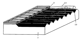
In Figure 7 a device is depicted comprising a substrate (7) on which
are integrated a layered optical waveguide component (3) and optical
fibre ends (13), the optical fibre ends being positioned in grooves
(10). The fibre ends (13) are connected to the facet (11) of the
waveguide (3). They are in vertical alignment with the guiding layer
(S) and laterally aligned with the channels (12) contained in the
guiding layer (5).
Figures 8-10 illustrate the interconnection of a flexible optical
waveguide component according to the invention with an optical
waveguide device.
In Figure 8 is depicted a flexible waveguide component (101)
comprising protective coating layers (102), deflection layers (103),
and a guiding layer (104). The guiding layer (104) is provided with
waveguide channels (105).
Figure 9 shows how the flexible waveguide component (101) includes an
interconnection section (106) which is devoid of the protective
coating (102) on one side (107) and provided with a rigid cover (108)
on the opposite side.
Figure 10 depicts the connection of component (101) with an optical
device (108) on a substrate (109).