Note: Descriptions are shown in the official language in which they were submitted.
2 1 9 8 5 J 2 1 CFO 11965 U5 ~
FABRICATION PROCESS OF SEMICONDUCTOR SUBSTRATE
BACKGROUND OF THE INVENTION
Field of the Invention
The present invention relates to a fabrication
process of semiconductor substrate and, more
particularly, to a process for fabricating a single-
crystal semiconductor on a dielectric isolation or an
insulator and a single-crystal compound semiconductor
on an Si substrate and further to a process for
fabricating a semiconductor substrate suitable for
electronic devices and integrated circuits made in a
single-crystal semiconductor layer.
Related Background Art
Formation of a single-crystal Si semiconductor
layer on an insulator is widely known as Si On
Insulator (SOI) technology and many researches have
been accomplished thereon, because devices obtained
utilizing the SOI technology have many advantages that
cannot be achieved by the normal bulk Si substrates for
fabrication of Si integrated circuits. Namely, use of
the SOI technology can enjoy the following advantages,
for example.
1. Dielectric isolation is easy and high
integration is possible.
2. Radiation resistance is high.
3. Stray capacitance is reduced and the operation
21 98552
speed can be enhanced.
4. The well process can be omitted.
5. Latch-up can be prevented.
6. Fully depleted field effect transistors can be
fabricated by thin-film structure.
These are described in further detail, for example, in
the following literature [Special Issue: "Single-
crystal silicon on non-single-crystal insulators";
edited by G. W. Cullen, Journal of Crystal Growth,
volume 63, no 3, pp 429-590 (1983)].
In these several years, many reports have been
presented on the SOI as a substrate to realize increase
of speed and decrease of consumption power of MOSFET
(IEEE SOI conference 1994). Since the SOI structure
has an insulating layer below devices, use thereof can
simplify the device isolation process as compared with
the cases for forming the devices on a bulk Si wafer,
which results in shortening the device process steps.
Namely, in addition to the increase in performance, the
total costs including the wafer cost and the process
cost are expected to be lowered than those of MOSFETs
and ICs on bulk Si.
Among others, the fully depleted MOSFETs are
expected to increase the speed and decrease the
consumption power because of an improvement in driving
force. The threshold voltage (Vth) of MOSFET is
determined in general by an impurity concentration of
21 ~S552
-- 3
the channel portion, and, in the case of the fully
depleted (FD) MOSFETs using the SOI, the thickness of a
depletion layer is also influenced by the film
thickness of the SOI. Accordingly, a strong desire
existed for evenness of the film thickness of SOI for
fabricating large-scale integrated circuits with good
yields.
On the other hand, the devices on a compound
semiconductor have high performance that cannot be
attained by Si, for example, high-speed operation,
radiation of light, and so on. Presently, most of
these devices are fabricated in a layer epitaxially
grown on a compound semiconductor substrate of GaAs or
the like. The compound semiconductor substrates,
however, have problems of being expensive, having low
mechanical strength, being not easy to fabricate a
large-area wafer, and so on.
Because of these problems, attempts have been made
to hetero-epitaxially grow a compound semiconductor on
the Si wafer, which is cheap, has high mechanical
strength, and permits fabrication of a large-area
wafer.
Returning the subject to the SOI structure,
researches on formation of SOI substrate have been
active since 70's. In the early stage many researches
were focused on a method for hetero-epitaxially growing
single-crystal Si on a sapphire substrate as an
2 1 9 8 5 J 2 4
insulator (SOS: Silicon on Sapphire), a method for
forming the SOI structure by dielectric isolation based
on oxidation of porous Si (FIPOS: Full Isolation by
Porous Oxidized Silicon), and an oxygen ion
implantation method.
The FIPOS method is a method for forming an n-type
Si layer in an island pattern on a surface of a p-type
Si single-crystal substrate by proton implantation
(Imai et al., J. Crystal Growth, vol 63, 547 (1983)) or
by epitaxial growth and patterning, making only the p-
type Si substrate porous from the surface so as to
surround Si islands by anodization in HF solution, and
then dielectric-isolating the n-type Si islands by
enhanced oxidation. This method has a problem that
degrees of freedom on device designing are limited,
because the Si regions isolated are determined prior to
the device processes.
The oxygen ion implantation method is a method
called SIMOX, which was first reported by K. Izumi.
Oxygen ions are first implanted in about 1017 to 1018/cm2
into an Si wafer and thereafter the wafer is annealed
at a high temperature of approximately 1320 ~C in an
argon-oxygen ambient. As a result, the oxygen ions
implanted around the depth corresponding to the
projected range (Rp) of ion implantation are bound with
Si to form an oxidized Si layer. On that occasion, an
Si layer, amorphized by the oxygen ion implantation
21 98552 5 _
above the oxidized Si layer, is also recrystallized to
form a single-crystal Si layer. Crystalline defects in
the surface Si layer were as many as 105/cm2 before, but
they were successfully decreased down to below 10Z/cm2
by adjusting the amount of implantation of oxygen to
near 4 x 10¹⁷/cm2. However, the film thicknesses of the
surface Si layer and the buried, oxidized Si layer
(BOX; Buried Oxide) were limited to specific values
because of narrow ranges of implantation energy and
implantation dose capable of maintaining the film
quality of the oxidized Si layer, crystallinity of the
surface Si layer, and so on. Sacrificial oxidation or
epitaxial growth was necessary for obtaining the
surface Si layer in a desired film thickness. In that
case, there is a problem that evenness of film
thickness is degraded, because degradation due to these
processes is added on the distribution of film
thickness.
It is also reported that malformed regions of
oxidized Si called pipes exist in the BOX. One of
causes thereof is conceivably contaminations such as
dust upon implantation. In the portions including the
pipes degradation of device characteristics occurs due
to leakage between the active layer and the support
substrate.
Since the implantation dose in the ion
implantation of SIMOX is larger than in the ion
2l q ~ 5 52 _ 6 -
implantation used for the normal semiconductor
processes as described previously, the implantation
time is still long even after dedicated equipment has
been developed. Since the ion implantation is carried
out by raster scan of an ion beam of a predetermined
electric current amount or by expanding the beam, an
increase in the implantation time is anticipated with
an increase in the area of wafer. In high-temperature
annealing of large-area wafer, it is pointed out that a
problem of generation of slip or the like due to the
temperature distribution within the wafer becomes
severer. Annealing at high temperatures, as high as
1320 ~C, which are not used normally in the Si
semiconductor processes is indispensable for the SIMOX,
and there is thus such a concern that the above problem
becomes further more significant, including development
of equipment.
Aside from the conventional SOI forming methods as
described above, attention is focused these years on
another method for bonding an Si single-crystal
substrate to another Si single-crystal substrate
thermally oxidized, by annealing or with an adhesive,
thereby forming the SOI structure. This method
requires evenly thinning the active layer for device.
In other words, it is necessary to thin the Si single-
crystal substrate even several hundred ~m thick down to
the order of ,um or less. The following three types of
21 9 8 ~ 5 2 7
methods are available for this thinning.
(1) thinning by polishing
(2) thinning by localized plasma etching
(3) thinning by selective etching
It is difficult to achieve uniform thinning by the
above polishing of (1). Especially, several ten ~ of
dispersion appears in thinning of sub-~m order, and
evening of this dispersion is a big problem. The
degree of its difficulty would increase more and more
with further increase in the diameter of wafer.
The above method of (2) is arranged to thin the
layer roughly by the method of polishing of (1) down to
about 1 to 3 ,um and to measure a distribution of film
thicknesses at multiple points over the entire surface.
After that, based on this distribution of film
thicknesses, the layer is etched as correcting the
distribution of film thicknesses by scanning it with a
plasma using SF6 or the like in the diameter of several
mm, whereby the layer is th;nn~d down to a desired film
thickness. It is reported that this method can achieve
the film thickness distribution of about l10 nm.
However, if there are contaminations (particles) on the
substrate upon plasma etching, the contaminations will
be an etching mask to form projections on the
substrate.
Since the surface is rough immediately after
etching, touch polishing is necessary after completion
21 ~8552 8
of the plasma etching. Control of polishing amount is
carried out by time management, and thus degradation of
control of final film thickness and of the film
thickness distribution by polishing is pointed out.
Further, because in polishing, an abrasive such as
colloidal silica directly rubs the surface to become
the active layer, concerns exist about formation of a
crush layer and introduction of work strain by
polishing. As the wafers further increase their area,
the time for plasma etching also increases in
proportion to the increase in the wafer area, which
also raises another concern about an extreme drop of
throughput.
The above method of (3) is a method for
preliminarily forming a selectively etchable film
structure in a substrate to be thinned. For example, a
thin layer of p+-Si cont~;~; ng boron in a concentration
of 1019 or more /cm3 and a thin layer of p-type Si are
stacked on a p-type substrate by the method of
epitaxial growth or the like, thereby obtaining a first
substrate. This is bonded to a second substrate
through an insulating layer of oxide film or the like
and thereafter the back face of the first substrate is
prel;~; n~rily thinned by grinding and polishing. After
that, the p+-layer is exposed by selective etching of
the p-type substrate and the p-type thin layer is
exposed by selective etching of the p+-layer, thus
2 1 9 ~ ~ 5 2 9
completing the SOI structure. This method is described
in detail in the report of Maszara (J. Electrochem.
Soc. 138, 341 (1991)).
Although the selective etching is said to be
effective for uniform thinning, it has the following
problems.
~The etch selectivity is not sufficient, at most
02 .
.It requires touch polishing after etching,
because the surface flatness after etching are poor.
This, however, results in decreasing the film thickness
and tends to degrade the uniformity of film thickness.
Especially, polish amounts are managed by time in
polishing, but polishing rates vary greatly, which
makes control of polish amount difficult. Accordingly,
a problem arises particularly in forming a very thin
SOI layer, for example, 100 nm thick.
~Crystallinity of the SOI layer is poor because of
use of the ion implantation and the epitaxial growth or
the hetero-epitaxial growth on the high-concentration-
B-doped Si layer. The surface flatness of the bonded
surfaces are inferior to the normal Si wafers.
Thus, the method of (3) has the above problems (C.
Harendt, et al., J. Elect. Mater. Vol. 20, 267 (1991),
H. Baumgart, et al., Extended Abstract of ECS 1st
International Symposium of Wafer Bonding, pp-733
(1991); C. E. Hunt, Extended Abstract of ECS 1st
21 98552 lo -
International Symposium of Wafer Bonding, pp-696
(1991)). Also, the selectivity of selective etching is
greatly dependent on concentration differences of
impurities of boron or the like and steepness of its
depthwise profile. Therefore, if high-temperature
bonding annealing is conducted in order to enhance the
bonding strength or if high-temperature epitaxial
growth is conducted in order to improve crystallinity,
the depthwise distribution of impurity concentration
will expand to degrade the etch selectivity. This
means that it was difficult to realize the both of an
improvement in the etch selectivity and an improvement
in the bonding strength.
Recently, Yonehara et al., solving such problems,
reported the bonding SOI excellent in uniformity of
film thickness and in crystallinity and capable of
being batch-processed (T. Yonehara, K. Sakaguchi and N.
Sato, Appl. Phys. Lett. 64, 2108 (1994)). This method
uses a porous layer 42 on an Si substrate 41, as a
material of selective etching. A non-porous single-
crystal Si layer 43 is epitaxially grown on the porous
layer and thereafter it is bonded to a second substrate
44 through an oxidized Si layer 45 (Fig. 14). The
first substrate is thinned from its back surface by a
method of grinding or the like, to expose the porous Si
42 across the entire surface of substrate (Fig. 15).
The porous Si 42 thus exposed is removed by etching
2 1 9 8 ~ 5 2 - 11
with a selective etchant such as KOH or HF + H202 (Fig.
16). At this time, the etch selectivity of porous Si
to bulk Si (non-porous single-crystal Si) is
sufficiently high, 100,000. Hence, the non-porous
single-crystal Si layer preliminarily grown on the
porous layer can be left on the second substrate with
little reduction of film thickness thereof, thus
forming the SOI substrate. Therefore, the uniformity
of film thickness of SOI is determined almost upon
epitaxial growth. Since the epitaxial growth allows
use of the CVD system used in the normal semiconductor
processes, it realized the uniformity thereof, for
example 100 nm + within 2 %, according to the report of
Sato et al. (SSDM 95). Also, the crystallinity of the
epitaxial Si layer was reported as good as 3. 5 x
102/cm2 .
Since in the conventional methods the etch
selectivity depended on the differences of impurity
concentration and the depthwise profile, temperatures
of thermal treatments (bonding, epitaxial growth,
oxidation, etc.) to expand the concentration
distribution were greatly restricted to below
approximately 800 ~C. On the other hand, in the
etching of this method, the etch rate is determined by
the difference of structure between porous and bulk,
and thus the restriction on the temperature of the
thermal treatments is little. It is reported that the
219~552 - 12 -
thermal treatment at about 1180 ~C is possible. For
example, annealing after bonding is known to enhance
the bonding strength between wafers and to decrease the
number and size of vacancies (voids) occurring in the
bonding interface. In such etching based on the
structural difference, particles deposited on porous Si
at the etching process, if present, do not affect the
uniformity of film thickness.
However, the semiconductor substrate using bonding
always requires two wafers, most of one of which is
wastefully removed and discarded by polishing, etching,
etc., which would result in wasting the limited Earth's
resources.
Accordingly, the SOI by bonding, according to the
existing methods, has a lot of problems in the aspects
of controllability, uniformity, and cost efficiency.
Recently, Sakaguchi et al. reported a method for
reusing the first substrate, which was consumed in the
above bonding method (Japanese Patent Application No.
07-045441 (1995)).
They employed the following method in place of the
step of thinning the first substrate from the back
surface by the method of grinding, etching, and the
like to expose porous Si in the bonding plus etchback
process using porous Si as described above.
A surface layer of first Si substrate 51 is made
porous to obtain a porous layer 52, a single-crystal Si
- 2198552 - 13 -
layer 53 is formed thereon, and this single-crystal Si
layer 53 and first Si substrate is bonded through an
insulating layer 55 with a principal surface of another
second Si substrate 54 (Fig. 17). After this, the
bonding wafer is divided at the porous layer (Fig. 18)
and the porous Si layer exposed in the surface on the
second Si substrate side is selectively removed,
thereby forming an SOI substrate (Fig. 19).
Division of the bonding wafer is effected by using
a method for breaking the porous Si layer, for example,
either one of a method for applying sufficient tension
or pressure perpendicularly to and uniformly in the
surface of the bonding wafer, a method for applying
wave energy of ultrasonic wave or the like, a method
for exposing the porous layer on the side face of
wafer, etching some of the porous layer, and inserting
an edge of a razor into the porous layer, a method for
exposing the porous layer on the side face of wafer,
infiltrating a liquid such as water into the porous Si
layer, and thereafter expanding the liquid by heating
or cooling the entire bonding wafer, and a method for
applying force horizontally onto the second (or first)
substrate relative to the first (or second) substrate,
or the like.
These methods are all based on an idea that the
mechanical strength of porous Si is sufficiently weaker
than bulk Si, though depending upon its porosity. For
2198552 - 14 -
example, with the porosity of 50 %, the mechanical
strength of porous Si may be considered to be the half
of that of bulk. Namely, when compression, tension or
shear force is exerted on the bonding wafer, the porous
Si layer is first broken. With increasing the porosity
the porous layer can be broken by weaker force.
However, when force is exerted vertically or
horizontally on the surface of wafer, the wafer is
sometimes elastically deformed to cause escape of
force, so as to fail to exert the force well on the
porous layer, depending upon a method of supporting the
wafer, because the semiconductor substrate is not a
perfectly rigid body, but an elastic body.
Similarly, with the method for inserting an edge
of a razor or the like through the side surface of
wafer, the yields were extremely lowered in some cases
unless the thickness of the razor was sufficiently thin
or unless the razor had sufficiently high rigidity.
Also, the razor was not able to be inserted uniformly
from the periphery or the force was exerted from the
outside on the bonding wafer, whereupon if the bond
strength of the bonding surface was weaker than the
strength of the porous Si layer or if there existed a
locally weak portion the two wafers were split at the
bonding surface, thereby sometimes failing to achieve
the initial purpose.
Accordingly, a desire exists for a method for
2198552 - 15 -
fabricating SOI substrates of sufficient quality with
good reproducibility and, at the same time, realizing
saving of resources and reduction of cost by re-use of
wafer or the like.
The bulletin of Japanese Laid-open Patent
Application No. 5-211128 (1993) describes a proposal of
a method for forming a bubble layer by ion
implantation, annealing it to cause rearrangement of
crystal and cohesion of bubbles, and dividing the wafer
through the bubble layer, wherein optimization of
annealing is not easy and it is carried out at low
temperatures of 400 to 600 ~C. Annealing at such low
temperatures cannot suppress generation of voids as
described above, and the voids once generated cannot be
nullified even with re-annealing at high temperature
after thinning. Namely, the decrease in the number and
size of voids is a phenomenon that occurs when the two
wafers are annealed at high temperature in the bonded
state, and high-temperature annealing after thinning
will increase the strength of the adhesive portion, but
will not decrease the voids.
The above description concerned the problems
related to the SOI technology by bonding, but there are
also demands as to the SOI technology for formation of
single-crystal layer on a light transparent substrate,
formation of a compound semiconductor layer on a
substrate, and so on, from the following reasons.
21 98552 16 -
Describing in detail, the light transparent
substrate is important in constructing contact sensors
being light receiving elements, and projection type
liquid crystal image display devices. Further, high-
performance drive elements are necessary for realizinghigher-density, higher-resolution, and higher-
definition of pixels (picture elements) in the sensors
and display devices. As a result, the devices provided
on the light transparent substrate need to be
fabricated using a single-crystal layer having
excellent crystallinity. Use of the single-crystal
layer enables peripheral circuits for driving the
pixels and circuits for image processing to be
incorporated in a same substrate as the pixels are,
thereby realizing size reduction and speed enhancement
of chip.
However, the light transparent substrate typified
by glass has disorderliness of its crystal structure in
general, and a thin Si layer deposited thereon is an
amorphous layer or, at best, a poly~Ly~al layer,
reflecting the disorderliness of substrate, of which
high-performance devices cannot be fabricated. Namely,
because of the crystal structure with many
imperfections, amorphous Si and poly~Ly~al Si are not
easy to fabricate drive elements having sufficient
performance that is required or will be required in
future. It is because the crystal structure of the
2198552 - 17 -
substrate is amorphous and simple deposition of Si
layer will not yield a single-crystal layer with good
quality.
On the other hand, substrates of compound
semiconductor are necessary and indispensable for
fabricating devices of compound semiconductor, but the
substrates of compound semiconductor are expensive and
very difficult to form a large area. From these
reasons, attempts have been made to hetero-epitaxially
grow a compound semiconductor of GaAs or the like on
the Si wafer, which can be fabricated as a large-area
wafer.
However, the thus grown film has poor
crystallinity because of differences of lattice
constant and coefficient of thermal expansion and it is
thus very difficult to apply it to devices.
It is, therefore, an object of the present
invention to provide a process for fabricating a film
with good crystallinity and to provide a process for
fabricating a semiconductor substrate, which can
effectively use the semiconductor substrate as a
material and which can suitably achieve saving of
resources and reduction of cost.
SUMMARY OF THE INVENTION
The inventor has been made strenuous efforts on
achieving the above object and achieved the following
21 98552 18 -
invention. Namely, a first fabrication process of
semiconductor substrate according to the present
invention is a fabrication process of semiconductor
substrate comprising: a step of bonding a principal
surface of a first substrate to a principal surface of
a second substrate, the first substrate being an Si
substrate in which at least one layer of non-porous
thin film is formed through a porous Si layer; a step
of exposing the porous Si layer in a side surface of a
bonding substrate comprised of the first substrate and
the second substrate; a step of dividing the bonding
substrate in the porous Si layer by oxidizing the
bonding substrate; and a step of removing a porous Si
and oxidized porous Si layer on the second substrate
separated by the division of the bonding substrate in
the porous Si layer.
Further, a second fabrication process of
semiconductor substrate according to the present
invention is a fabrication process of semiconductor
substrate comprising: a step of bonding a principal
surface of a first substrate to a principal surface of
a second substrate, the first substrate being an Si
substrate in which at least one layer of non-porous
thin film is formed through a porous Si layer and in
which the porous Si layer is exposed in a side surface
thereof; a step of dividing the bonding substrate in
the porous Si layer by oxidizing a bonding substrate
comprised of the first substrate and the second
2198552 - 19
substrate; and a step of removing a porous Si and
oxidized porous Si layer on the second substrate
separated by the division of the bonding substrate in
the porous Si layer.
Also, a third fabrication process of semiconductor
substrate according to the present invention is one
according to the above first or second fabrication
process of semiconductor substrate, wherein after
removing the porous Si and oxidized porous Si layer on
the first substrate separated by the division of the
bonding substrate in the porous Si layer, the first
substrate is again used as a raw material for the first
substrate before bonding.
In addition, a fourth fabrication process of
semiconductor substrate according to the present
invention is one according to the above first or second
fabrication process of semiconductor substrate, wherein
after removing the porous Si and oxidized porous Si
layer on the first substrate separated by the division
of the bonding substrate in the porous Si layer, the
first substrate is again used as a raw material for the
second substrate before bonding.
Moreover, a fifth fabrication process of
semiconductor substrate according to the present
invention is one according to either one of the above
first to fourth fabrication processes of semiconductor
substrate, wherein at least one layer of non-porous
thin film is formed through a porous Si layer on each
21 98 5 52 - 20 -
of two principal surfaces of the first substrate and
the second substrate is bonded to each of the two
principal surfaces.
The present invention utilizes enhanced oxidation
of porous Si to oxidize the porous Si layer from the
periphery of wafer, whereby volume expansion of porous
Si becomes greater from the center to the periphery.
This seems as if porous Si is uniformly wedged from the
periphery, so that the internal pressure is exerted on
only the porous layer, and it splits the wafer in the
porous Si layer therethrough across the entire surface
of wafer. This provides the fabrication process of
semiconductor substrate solving the various problems as
discussed previously.
Namely, in the case of the bonding substrate
having the multi-layered structure, if the method of
splitting at porous Si by external pressure is applied
and if the substrate has an interface with low strength
or a partially weak region, the substrate will be split
at the weak portion. In contrast, the present
invention permits the internal pressure to be exerted
only on the porous Si layer by utilizing oxidation, one
step of the normal Si-IC processes, excellent in
uniformity, and by combining high-speed oxidizability
of porous Si, volume expansion of porous Si, and
fragility of porous Si, whereby the wafer can be split
with good controllability in and through the porous Si
2198552 - 21 -
layer.
Further, use of the process according to the
present invention enables to reuse the first Si
substrate after removal of the porous substrate
portion. This first Si substrate can be reused any
number of times before it becomes unusable in respect
of its mechanical strength.
The present invention permits separation through
the porous layer over a large area in removing the
first Si substrate. The first Si substrate thus
removed can be reused again as a first Si substrate or
as a next second substrate after removing the residual
porous layer or after flattening the surf.ace if the
surface is so rough that its surface flatness is not
permissible. The surface flattening process may be the
method of polishing, etching, etc. used in the normal
semiconductor processes, but may be annealing in an
ambient containing hydrogen. By selecting suitable
conditions for this annealing, the surface can be
flattened so as to reveal atomic steps locally. In the
case of repetitive use as a first Si substrate, this
first Si substrate can be reused any number of times
before it becomes unusable in respect of mechanical
strength.
Since the present invention permits division of a
large area en bloc through the porous layer, it can
obviate the need for the grinding, polishing, and
- 21 98552 22 -
etching steps conventionally essential for removing the
first substrate to expose the porous Si layer, thereby
decreasing the steps. In addition, the position of
division can be defined at a limited depth in the
porous Si layer by preliminarily performing ion
implantation of at least one element out of rare gases,
hydrogen, and nitrogen so as to have the projected
range in the porous layer, which evens the thickness of
the porous layer remaining on the second substrate
side. Then the porous layer can be removed uniformly
even with an etchant having an etch selectivity not so
high. Further, the conventional fabrication of bonding
substrate employed the method for successively removing
the first Si layer from one surface by gr;n~;~g and
etching, and therefore, it was impossible to bond the
two surfaces of the first Si layer with respective
support substrates, as effectively utilizing the both
surfaces. In contrast, according to the present
invention, the first Si substrate except for the
surface layer thereof is maintained as it was, and two
substrates fabricated by bonding, deviding and thinning
can be fabricated simultaneously with the aid of one
first Si substrate by using the both surfaces of the
first Si substrate as principal surfaces and bonding
support substrates to the respective surfaces, which
can raise productivity. Of course, the first Si
substrate after division can be reused.
2198~2 - 23 -
In addition, the present invention permits a large
area to be divided en bloc through the porous layer in
removing the first Si substrate, which can decrease the
steps, which is economically excellent, and which can
transfer a non-porous thin film such as an Si single-
crystal layer or a compound semiconductor single-
crystal layer being uniformly flat across a large area
and having extremely excellent crystallinity to the
second substrate at a good yield. Namely, the SOI
structure with the Si single-crystal layer formed on
the insulating layer can be attained with good
uniformity of film thickness and at a good yield.
In other words, the present invention provides the
Si single-crystal layer or the compound semiconductor
single-crystal layer with the remarkably reduced number
of imperfections on the insulator by using the Si
single-crystal substrate being economically excellent,
being uniformly flat across a large area, and having
extremely excellent crystallinity and by removing the
portion ranging from its one surface to the active
layer as leaving the Si or compound semiconductor
active layer formed in the surface.
The present invention provides the fabrication
process of semiconductor substrate superior in the
aspects of productivity, uniformity, controllability,
and cost in obtaining the Si or compound semiconductor
single-crystal layer with excellent crystallinity
2 1 q8552 - -
equivalent to that of single-crystal wafer, on a
transparent substrate (light transmissive substrate).
The fabrication process of semiconductor substrate
according to the present invention involves performing
selective etching with outstandingly excellent etch
selectivity, thereby enabling to obtain an Si single
crystal or compound semiconductor single crystal being
uniformly flat across a large area and having extremely
excellent crystallinity.
Further, removal of the porous Si layer of the
present invention can also be done by selective
polishing with using the single-crystal layer as a
polishing stopper because porous Si has low mechanical
strength and enormous surface area.
Also, the present invention can provide the
fabrication process of semiconductor substrate that can
replace the expensive SOS or SIMOX for fabricating
large-scale integrated circuits of the SOI structure.
The present invention can form a single-crystal
compound semiconductor layer with good crystallinity on
porous Si, can transfer the semiconductor layer onto an
economically excellent and large-area insulating
substrate, and can form the compound semiconductor
layer with good crystallinity on the insulating
substrate as well restraining the differences of
lattice constant and coefficient of thermal expansion
which were the forgoing problems.
2 1 ~8552 25 -
In the present invention, a layer of a material
having a smaller coefficient of thermal expansion than
that of Si is formed at least on one side of the outer
surfaces of the bonding substrate before splitting by
oxidation (or possibly before bonding), whereby at
temperatures during oxidation Si becomes more likely to
expand and thus stress acts in the wafer peeling
directions in the peripheral region of the bonding
wafer, facilitating occurrence of the wedge effect by
oxidation.
Also, in the case wherein regions without an
implant layer formed are formed because of existence of
contaminations on the surface upon ion implantation,
because the mechanical strength of the porous layer
itself is smaller than that of bulk Si, peeling occurs
in the porous layer, so that the two substrates bonded
can be divided without extending damages such as cracks
to the non-porous single-crystal Si layer.
Since the ion implant region has the gettering
effect, metal impurities, if present, can be subject to
gettering by the ion implant region and thereafter the
ion implant region with the impurities can be removed
by separating the two substrates bonded. It is thus
effective to impurity contamination.
The present invention may combine anodization with
ion implantation to make the porosity of the side
surface small and the porosity of the central part
2198552 - 26 -
large, thereby making the volume expansion of the side
surface greater and the strength of the central part
low so as to facilitate peeling.
BRIEF DESCRIPTION OF THE DRAWINGS
Fig. 1 is a schematic cross-sectional view for
explaining the principle of the present invention;
Fig. 2 is a schematic cross-sectional view for
explaining the principle of the present invention;
Fig. 3 is a schematic cross-sectional view for
explaining the principle of the present invention;
Fig. 4 is a schematic cross-sectional view for
explaining a step of the present invention;
Fig. 5 is a schematic cross-sectional view for
explaining a step of the present invention;
Fig. 6 is a schematic cross-sectional view for
explaining a step of the present invention;
Fig. 7 is a schematic cross-sectional view for
explaining a step of the present invention;
Fig. 8 is a schematic cross-sectional view for
explaining a step of the present invention;
Fig. 9 is a schematic cross-sectional view for
explaining a step of the present invention;
Fig. 10 is a schematic cross-sectional view for
explaining a step of the present invention;
Fig. 11 is a schematic cross-sectional view for
explaining a step of the present invention;
2198552 - 27 -
Fig. 12 is a schematic cross-sectional view for
explaining a step of the present invention;
Fig. 13 is a schematic cross-sectional view for
explaining a step of the present invention;
Fig. 14 is a schematic cross-sectional view for
explaining a step of the conventional example;
Fig. 15 is a schematic cross-sectional view for
explaining a step of the conventional example;
Fig. 16 is a schematic cross-sectional view for
explaining a step of the conventional example;
Fig. 17 is a schematic cross-sectional view for
explaining a step of another conventional example;
Fig. 18 is a schematic cross-sectional view for
explaining a step of another conventional example;
Fig. 19 is a schematic cross-sectional view for
explaining a step of another conventional example.
DETAILED DESCRIPTION OF THE PREFERRED EMBODIMENTS
In the present invention, the porous Si layer is
oxidized from the periphery of wafer, utilizing
enhanced oxidation of porous Si. Volume expansion of
porous Si increases from the center toward the
periphery, and the present invention thus has the same
effect as porous Si is as if to be uniformly wedged
from the periphery. In that case, the internal
pressure is exerted on only the porous Si layer and the
wafer is divided in the porous Si layer throughout the
21~8552 - 28 -
entire surface. This provides the fabrication process
of semiconductor substrate solving the various problems
as discussed previously.
The principle of division by oxidation as a basis
of the present invention will be described with
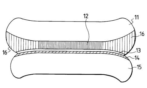
reference to Fig. 1 to Fig. 3. In Fig. 1 to Fig. 3,
reference numeral 11 designates a first Si single-
crystal substrate; 12, a porous Si layer; 13, a non-
porous thin film; 14, an insulating layer; 15, a second
substrate; and 16, an oxidized porous Si layer.
Although Fig. 1 to Fig. 3 illustrate an embodiment in
which the insulating layer has been formed on the
surface of the second substrate, it may be formed on
the first substrate or both of the first and second
ones. There are some such cases as GaAs on Si p-n
junction where the insulating layer has been formed on
neither of the substrate. Fig. 1 shows a bonding
substrate immediately before oxidation. The side
surface of porous Si is exposed. The side surface of
porous Si is also normally covered by a non-porous thin
film, and it is necessary to make the side surface
exposed after or before bonding. When this bonding
substrate is oxidized, enhanced oxidation starts from
the side surface of porous Si because of the enormous
surface area of porous Si. The volume expands 2.27
times when Si turns to SiO2. Thus, if the porosity is
not more than 56 %, then the volume of the oxidized,
- 2! 98552 29 -
porous Si layer will expand. The nearer the position
to the center of wafer, the lower the degree of
oxidation. Thus, the volume expansion of the oxidized
porous Si layer near the side surface of wafer bec
greater as shown in Fig. 2. This is just the same
condition as wedges are driven into the porous Si layer
from the side surface of wafer, and the internal
pressure is exerted on only the porous Si layer, so
that force acts so as to divide the substrate in porous
Si. In addition, since oxidation uniformly progresses
at the periphery of wafer, the bonding wafer will be
split equally from the circumference of wafer. As a
result, the wafer is divided as shown in Fig. 3. This
oxidation step is a step used in the normal Si-IC
processes and thus requires neither special facilities
nor special techniques such as careful insertion of an
edged tool.
The bonding substrate has the multi-layered
structure, and, thus, if it has an interface of low
strength or a locally weak region, the method of
splitting at porous Si by external pressure would cause
splitting at the weak portion. The present invention
permits the internal pressure to be exerted on only the
porous Si layer, utilizing one step, oxidation, with
excellent uniformity of the normal Si-IC processes and
combining the enhanced oxidizability of porous Si,
volume expansion of porous Si, and fragility of porous
2 1 98552 - -
Si, whereby the wafer can be divided with good
controllability in the porous Si layer.
After the residual porous Si and oxidized porous
Si layer is removed from the first Si substrate thus
separated by the above method of the present invention,
the first Si substrate is subjected to a surface
flattening process if surface flatness thereof is
insufficient. Then the first Si substrate can be
reused again as a first Si layer or as a next second
substrate.
The surface flattening process may be the method
of polishing, etching, and the like used in the normal
semiconductor processes, but may be annealing in an
ambient containing hydrogen. By properly selecting the
conditions for this ~nn~.~l ing, the substrate can be
flattened so as to expose atomic steps locally. The
~n"e~ling in the ambient containing hydrogen may be
carried out, for example, under such conditions as H2
100 %, 1100 ~C, 2 hours; Hz/Ar = 20/80, 1150 ~C, 1 hour;
or H2 100 %, 1050 ~C, 2 hours.
Since the present invention permits a large area
to be divided en bloc through the porous layer, it can
omit the grinding, polishing, and etching steps that
were conventionally essential for removing the first
substrate to expose the entire surface of porous Si
layer, thus decreasing the steps.
When the substrate separated is repetitively used
2198552 - 31 -
as a first Si substrate, this first Si substrate can be
reused any number of times before it becomes unusable
in the aspect of mechanical strength.
Further, since the conventional fabrication of
bonding substrate employs the method for successively
removing the first Si substrate from one side thereof
by grinding and etching, it is impossible to bond the
both surfaces of the first Si substrate to respective
support substrates as effectively utilizing the two
surfaces. In contrast with it, according to the
present invention, the first Si substrate except for
the surface layer is maintained in its original state,
and thus, by using the both surfaces of the first Si
substrate as principal surfaces and bonding the two
surfaces to the respective support substrates, two
substrates fabricated by bonding, deviding, and
thinning can be simultaneously fabricated from one
first Si substrate, which can decrease steps and
improve productivity. Of course, the first Si
substrate separated can be reused.
In other words, the present invention provides the
Si single-crystal layer or the compound semiconductor
single-crystal layer with the remarkably reduced number
of imperfections on the insulator by using the Si
single-crystal substrate being economically excellent,
being uniformly flat across a large area, and having
extremely excellent crystallinity and by removing the
- 2 1 ~ 8 5 52 - 32 -
portion ranging from its one surface to the active
layer as leaving the Si or compound semiconductor
active layer formed in the surface.
The present invention provides the fabrication
process of semiconductor substrate superior in the
aspects of productivity, uniformity, controllability,
and cost in obt~; n; ng the Si or compound semiconductor
single-crystal layer with excellent crystallinity
equivalent to that of single-crystal wafer, on a
transparent substrate (light transparent substrate).
Also, the present invention provides the
fabrication process of semiconductor substrate that can
replace the expensive SOS or SIMOX for fabricating
large-scale integrated circuits of the SOI structure.
The present invention can form a single-crystal
compound semiconductor layer with good crystallinity on
porous Si, can transfer the semiconductor layer onto an
economically excellent and large-area insulating
substrate, and can form the compound semiconductor
layer with good crystallinity on the insulating
substrate as well restraining the differences of
lattice constant and coefficient of thermal expansion
which were the above-stated problems.
Further, removal of the porous Si layer of the
present invention can also be done by selective
polishing with using the single-crystal layer as a
polishing stopper because porous Si has low mechanical
- 21q85~2 33 -
strength and enormous surface area.
The present invention may combine anodization with
ion implantation to make the porosity of the side
surface small and the porosity of the central part
large, thereby making the volume expansion of the side
surface greater and the strength of the central part
low so as to facilitate peeling.
In the present invention, a layer of a material
having a smaller coefficient of thermal expansion than
that of Si is formed at least on one side of the outer
surfaces of the bonding substrate before splitting by
oxidation (or possibly before bonding), whereby at
temperatures during oxidation Si becomes more likely to
expand and thus stress acts in the wafer peeling
directions in the peripheral region of the bonding
wafer, facilitating occurrence of the wedge effect by
oxidation.
The present invention simultaneously solves the
various problems discussed previously by the above-
stated enhanced oxidation and volume expansion ofporous layer effected uniformly from the periphery of
wafer.
Uhlir et al. discovered porous Si during the
research process on electrolytic polishing of
semiconductor in 1956 (A. Uhlir, Bell Syst. Tech. J.,
vol. 35, 333 (1956)). Porous Si can be formed by
anodizing an Si substrate in HF solution. Unagami et
2198552 - 34 ~
al. studied dissolution of Si in the anodization and
reported that the anode reaction of Si in HF solution
required holes and that the reaction was as follows (T.
Unagami, J. Electrochem. Soc., vol. 127, 476 (1980)).
Si + 2HF + (2 - n)e~ ~ SiF2 + 2H~ + ne~
SiF2 + 2HF ~ SiF4 + H2
SiF4 + 2HF ~ H2SiF6
or
Si + 4HF + (4 - ~)e~ ~ SiF4 + 4H' + ~e~
SiF4 + 2HF ~ H2SiF6
Here, e~ and e~ represent a hole and an electron,
respectively. Further, each of n and ~ is the number
of holes necessary for one atom of Si to dissolve, and
it is reported that porous Si is formed when the
condition of n > 2 or ~ > 4 is satisfied.
From the foregoing, p-type Si including holes can
be changed to porous Si, but n-type Si cannot. The
selectivity in this porous Si formation was verified by
Nagano et al. and Imai (Nagano, Nakajima, Anno, Onaka,
and Kajiwara, technical research report, the Institute
of Electronics, Information and Communication Engineers
(IEICE), vol. 79, SSD 79-9549 (1979)) and (K. Imai,
Solid-State Electronics, vol. 24, 159 (1981)).
There is, however, another report telling that
heavily doped n-type Si can be changed to porous Si (R.
P. Holmstrom and J. Y. Chi, Appl. Phys. Lett., vol. 42,
386 (1983)) and it is thus important to select a
2l 98 5 52 ~ 35 ~
substrate that can realize porous Si formation without
adhering to the difference between p-type and n-type.
Porous Si can be formed by anodization of the Si
substrate in HF solution. The porous layer has a
spongelike structure in which pores with diameters
ranging approximately from 10~1 to 10 nm are arranged at
intervals of about 10~1 to 10 nm. The density thereof
can be changed in the range of 2.1 to 0.6 g/cm3 by
changing the concentration of HF solution in the range
of 50 to 20 % or by changing the current density, in
comparison with the density of single-crystal Si 2.33
g/cm3. Namely, the porosity can vary. Although the
density of porous Si is below the half of that of
single-crystal Si as described, it maintains the single
crystal property and it is also possible to epitaxially
grow a single-crystal Si layer on the porous layer.
However, temperatures over 1000 ~C cause rearrangement
of internal pores, which will impair the characteristic
of enhanced etching. Therefore, the epitaxial growth
of Si layer is preferably low temperature growth
selected from the molecular beam epitaxial growth,
plasma enhanced CVD, low pressure CVD, photo assisted
CVD, bias sputter process, liquid phase growth, and so
on. However, high-temperature growth is also possible
if a protective film is preliminarily formed over the
pore walls of the porous layer by a method of low-
temperature oxidation or the like.
- 21 q8552 36 -
Since a lot of pores are formed inside the porous
layer, the density of the porous layer decreases to the
half or less. As a result, the surface area
outstandingly increases as compared with the volume,
and thus its chemical etching rate is remarkably
enhanced as compared with the etching rates of normal
single-crystal layer.
The mechanical strength of porous Si is considered
to be lower than that of bulk Si, though depending upon
the porosity. For example, if the porosity is 50 %,
the mechanical strength can be considered to be the
half of bulk. Namely, when compression, tension or
shear force is exerted on the bonding wafer, the porous
Si layer will be first broken. With increasing the
porosity the porous layer can be broken by weaker
force.
It is reported that after ions of helium or
hydrogen are implanted into bulk Si, followed by
annealing, micro-cavities with diameters of several nm
to several ten nm are formed in the density of even
10l6~17/cm3in the implant region (for example, A. Van
Veen, C. C. Griffioen, and J. H. Evans, Mat. Res. Soc.
Symp. Proc. 107 (1988, Material Res. Soc. Pittsburgh,
Pennsylvania) p. 449). It is recently researched to
utilize the micro-cavities as gettering sites of metal
impurities.
V. Raineri and S. U. Campisano implanted helium
2198552 - 37 ~
ions into bulk Si and ~nne~led it to form the cavities.
Thereafter, they formed a groove in the substrate to
expose the side surface of the cavities and subjected
it to oxidation. As a result, the cavities were
selectively oxidized to form a buried, oxidized Si
layer. Namely, they reported formation of the SOI
structure thereby (V. Raineri, and S. U. Canpisano,
Appl. Phys. Lett. 66 (1995) p. 3654). Their method,
however, failed to form the SOI structure over the
entire surface of substrate because the thicknesses of
the surface Si layer and buried, oxidized Si layer are
limited to those that can effect the both of formation
of cavities and relaxation of stress introduced due to
volume expansion upon oxidation together and because
formation of groove is necessary for selective
oxidation. Such formation of cavities has been
reported as a phenomenon occurring with injection of
light element into metal, together with swell and
peeling phenomena of these cavities, in part of
researches related to the first wall of fusion reactor.
The second substrate may be selected, for example,
from an Si substrate, an Si substrate with an oxidized
Si film formed thereon, light transparent substrates
such as a ~uartz substrate (silica glass) or a glass
substrate, and metal substrates, but it is not limited
particularly to these.
The thin film formed on the porous Si layer on the
2198552 - 38 -
first substrate may be selected, for example, from
metal thin films and carbon thin films as well as non-
porous single-crystal Si and the compound
semiconductors such as GaAs or InP, but it is not
limited to these. Further, it is not essential that
the thin film of these be formed over the entire
surface, and it may be partially etched by a patterning
process.
The bonding wafer of Si has advantages of being
oxidized at high temperatures and simultaneously
annealed at high temperatures for reduction of voids.
Embodiments of the present invention will be
explained.
[Embodiment 1]
As shown in Fig. 4, a first Si single-crystal
substrate 21 is first prepared and then at least one
non-porous thin film 23 and a porous Si layer 22
immediately under it are formed over the outermost
surface layer of the principal surface thereof. A
procedure for fabricating the non-porous thin film 23
and porous Si layer 22 is either one selected from the
following procedures.
a) forming the porous Si layer 22 by anodization
and forming the non-porous thin film 23;
b) implanting ions of at least one element
selected from rare gases, hydrogen, and nitrogen into
the substrate to simultaneously form the porous Si
2 ! 9 8 ~ J 2 39
layer 22 and the non-porous thin film 23;
c) in addition to a), further implanting ions of
at least one element selected from rare gases, hydrogen
and nitrogen into the substrate to make another region
with a different porosity.
The non-porous thin film 23 is arbitrarily
selected from single-crystal Si, polycrystal Si,
amorphous Si, or metal films, compound semiconductor
thin films, superconductive thin films, and so on. Or,
even the device structure of MOSFET or the like may be
formed. Further, formation of SiO2 as an outermost
layer is preferred from the reason why the interface
state of the bonding interface can be separated away
from the active layer (though SiO2 does not always have
to be provided). Observation of the implant layer with
a transmission electron microscope confirms that an
infinite number of micro-cavities are formed. There is
no specific limitations on the charge state of implant
ions. The acceleration energy is so set that the
projected range is coincident with a depth desired to
implant. The size and density of micro-cavities formed
vary depending upon an implant amount, but the density
is approximately 1 x 10¹⁴/cm2 or more, more preferably 1
x 1015/cm2. If the projected range is desired to set
deeply, channeling ion implantation may be applied.
After implantation, annealing is carried out as
occasion demands. As shown in Fig. 5, the second
21 98552 40 _
substrate 24 is made in close contact with the surface
of the first substrate at room temperature. After
that, bonding may be enhanced by anodic bonding,
pressing, or annealing with necessity, or a combination
thereof.
If single-crystal Si is deposited, it is preferred
to form oxidized Si by a method of thermal oxidation or
the like over the surface of single-crystal Si and then
to bond it to the second substrate. The second
substrate may be selected from Si, a substrate obtained
by forming an oxidized Si film on an Si substrate,
light transparent substrates of quartz or the like,
sapphire, and the like, but it is not limited to these.
The point is that a surface thereof to be bonded is
sufficiently flat.
The two substrates may be bonded in the three-
plate laminate structure with an insulating thin plate
inbetween.
A layer of a material having a smaller coefficient
of thermal expansion than Si may be formed on at least
one side of the outer surfaces of the bonding substrate
before splitting by oxidation (or possibly before
bonding). At temperatures during oxidation Si becomes
easier to expand and stress acts in the wafer peeling
directions around the periphery of the bonding wafer,
thereby supplementing the wedge effect by oxidation.
The side surface of the porous Si layer is made to
- 21 98552 41 -
be exposed by either one of methods of etching the non-
porous thin film 23 after bonding, etching it before
bonding, and preventing the non-porous thin film 23
from being formed on the side surface. The bonding
substrate is oxidized to subject porous Si of the side
surface to enhanced oxidation. (In the drawing numeral
25 designates oxidized porous Si.) Then, as shown in
Fig. 6, volume expansion of side-surface porous Si
causes stress to act so as to peel the porous Si layer
and, finally, to divide the substrate in the porous Si
layer 22 (Fig. 7). The second substrate side has the
structure of porous Si 22 + oxidized porous Si 25 /
non-porous thin film (single-crystal Si layer, for
example) 23 / second substrate 24.
Further, the porous Si 22 and oxidized porous Si
25 is selectively removed. Oxidized porous Si 25 is
etched with hydrofluoric acid solution. When the non-
porous thin film is of single-crystal Si, only porous
Si 22 is etched by electroless wet chemical etching
with at least one etchant selected from ordinary Si
etchants, hydrofluoric acid being an etchant for
selective etching of porous Si, a mixture solution
obtained by adding at least one of alcohol (ethyl
alcohol, isopropyl alcohol, etc.) and hydrogen peroxide
solution to hydrofluoric acid, buffered hydrofluoric
acid, and a mixture solution obtained by adding at
least one of alcohol and hydrogen peroxide to buffered
21 98552
- 42 -
hydrofluoric acid, thereby leaving the film
preliminarily formed on the porous layer of first
substrate, on the second substrate. As detailed above,
only porous Si can be selectively etched even with the
ordinary Si etchant because of the enormous surface
area of porous Si. Alternatively, porous Si 22 is
removed by selective polishing with using the non-
porous thin film layer 23 as a polishing stopper.
When a compound semiconductor layer is formed on
the porous layer, only porous Si 22 is chemically
etched with an etchant having a faster etch rate of Si
than that of the compound semiconductor, thereby
leaving and, thus forming, the thinned single-crystal
compound semiconductor layer 23 on the second substrate
24. Alternatively, porous Si 22 is removed by
selective polishing with using the single-crystal
compound semiconductor layer 23 as a polishing stopper.
Fig. 8 shows a semiconductor substrate obtained by
the present invention. A non-porous thin film, for
example, a single-crystal Si thin film 23, is formed,
as thinned flatly and uniformly, in a large area
throughout the entire region of wafer on the second
substrate 24. If an insulating substrate is used as
the second substrate 24, the semiconductor substrate
thus obtained can be suitably used also from the
viewpoint of fabrication of dielectric-isolated
electronic devices.
21 ~8552 43 _
The first Si single-crystal substrate 21 can be
reused again as a first Si single-crystal substrate 21
or as a next second substrate 24 after the residual
porous Si and oxidized porous Si layer is removed and,
if the surface thereof is so rough that the surface
flatness thereof is not permissible, after the surface
thereof is flattened.
[Embodiment 2]
As shown in Fig. 9 to Fig. 13, the above step
described in Embodiment 1 is applied to the both
surfaces of the first substrate with two second
substrates, thereby fabricating two semiconductor
substrates simultaneously.
In Fig. 9 to Fig. 13, reference numeral 31
designates a first Si single-crystal substrate; 32,
porous Si layers provided on the both principal
surfaces of the first Si single-crystal substrate 31;
33, non-porous thin films provided on the porous Si
layers 32; 34 and 35, second substrates; and 36,
oxidized porous Si layers.
The first Si single-crystal substrate 31 can be
reused again as a first Si single-crystal substrate 31
or as a next second substrate 34 (or 35) after residual
porous Si is removed or, if the surface is so rough
that the surface flatness is not permissible, after the
surface is flattened.
The support substrates 34, 35 do not have to be
2198552 - 44 ~
those of the same conditions (material, thickness,
etc.).
The non-porous thin-films 33 on the both surfaces
do not have to be of the same conditions (material,
thickness, etc.).
EXAMPLES
Examples of the present invention will be
described.
(Example 1)
Prepared was a p-type or n-type 6-inch-diameter
first (100) single-crystal Si substrate having the
thickness of 625 ,um and the specific resistance of 0.01
Q-cm, and it was subjected to anodization in HF
solution. The conditions for the anodization were as
follows.
Current density: 7 (mA-cm~2)
Anodization solution: HF:H20:C2H50H = 1:1:1
Time: 11 (min)
Thickness of porous Si: 12 (~m)
Porosity: 15 (~)
This substrate was oxidized at 400 ~C in an oxygen
ambient for one hour. This oxidation caused a
thermally oxidized film to cover the internal walls of
pores of porous Si. Single-crystal Si was epitaxially
grown in the thickness of 0.15 ,um on porous Si by the
CVD (Chemical Vapor Deposition) process. The growth
conditions were as follows.
2l ~ 8 5 52 ~ 45 -
Source gas: SiH2C12/H2
Gas flow rate: 0.5/180 l/min
Gas pressure: 80 Torr
Temperature: 950 ~C
Growth rate: 0.3 ~um/min
Further, an SiO2 layer of 100 nm was formed over
the surface of this epitaxial Si layer by thermal
oxidation.
The surface of this SiO2 layer was laid on and made
into contact with a surface of an Si substrate (second
substrate) with an SiO2 layer of 500 nm formed
thereover, separately prepared. After contact of the
surfaces, the SiO2 layer of lOOnm and the epitaxial Si
layer were remored by etching on the side surface of
the bonding wafer, which exposed the edge of porous Si.
The bonding wafer was pyro-oxidized at 1000 ~C,
and it was divided perfectly in the porous Si layer
into two substrates after one hour. The separated
surfaces were observed, showing that the central
portion was found to remain almost in its original
state while porous Si of the wafer side surface was
changed to SiO2.
After that, the porous Si and oxidized porous Si
layer remaining on the second substrate side was
subjected to selective etching with agitation in a
mixture solution of 49 % hydrofluoric acid and 30 %
hydrogen peroxide solution. Single-crystal Si remained
2! 98552
- 46 -
without being etched, and with the single-crystal Si as
a material of etch stop the porous Si and oxidized
porous Si layer was selectively etched to be removed
completely.
The etch rate of non-porous Si single crystal by
the etchant was extremely low and the selectivity of
the etch rate of the porous layer thereto was even 105
or more. Therefore, a decrease in film thickness of
the non-porous layer was so small that the etch amount
thereof was practically ignorable (about several ten
angstroms).
Namely, the single-crystal Si layer was formed in
the thickness of 0.1 ~m on the Si oxide film. Film
thicknesses of the single-crystal Si layer thus formed
were measured at 100 points across the entire surface,
and uniformity of film thickness was 101 nm + 3 nm.
Further, it was annealed at 1100 ~C in hydrogen
for one hour. Surface roughness was evaluated with an
atomic force microscope and the root mean square
roughness in a region 50 ,um square was approximately
0.2 nm, which was equivalent to those of Si wafers
commercially available.
Observation of cross section with a transmission
electron microscope resulted in confirming that no new
crystal defects were introduced into the Si layer and
that good crystallinity was maintained.
The present example showed an example in which the
2198552 - 47 -
oxide film was formed in the surface of the epitaxial
Si layer and in which the oxide film was also formed in
the surface of the second substrate (i.e., the oxide
film was formed in the both substrates), but the same
results were attained in the cases wherein the oxide
film was provided in either one substrate and wherein
the oxide film was not provided in either substrate.
However, as discussed previously, formation of the
oxide film over the outermost layer of the epitaxial Si
layer is preferable from the point that the interface
state of the bonding interface is able to be separated
away from the active layer.
In fact, it was also the case in the subsequent
embodiments that the same results were attained in any
cases wherein the oxide film was formed in the both
substrates, wherein the oxide film was formed in either
one of the substrates, and wherein the oxide film was
not formed in either substrate. Then, it is also the
case that formation of the oxide film over the
outermost layer of non-porous thin film (epitaxial Si
layer) is preferable from the point that the interface
state of the bonding interface can be separated away
from the active layer.
(Example 2)
Prepared was a p-type or n-type 6-inch-diameter
first (100) single-crystal Si substrate having the
thickness of 625 ~m and the specific resistance of 10
2 1 9 8 ~ 5 2 48 -
Q-cm, and an SiO2 layer of 100 nm was formed over the
surface thereof by thermal oxidation. Hydrogen ions
were implanted in 1 x 10¹⁷/cm2 into the principal
surface with the acceleration voltage of 50 keV
applied. This resulted in forming a porous structure
in the depth of near 0.5 ~m below the surface by
hydrogen bubbles.
The surface of this SiO2 layer was laid on and made
into contact with a surface of an Si substrate (second
substrate) with an SiO2 layer of 500 nm formed
thereover, separately prepared. After contact of the
surfaces, the SiO2 layer of 100 nm and the epitaxial Si
layer were removed by etching on the side surface of
the bonding wafer, which exposed the edge of porous Si.
The bonding wafer was pyro-oxidized at 1000 ~C,
and it was divided perfectly in the porous Si layer
into two substrates after one hour. The separated
surfaces were observed, showing that the central
portion was found to remain almost in its original
state while porous Si of the wafer side surface was
changed to SiO2.
After that, the porous Si and oxidized porous Si
layer rem~; n; ng on the second substrate side was
subjected to selective etching with agitation in the
mixture solution of 49 % hydrofluoric acid and 30 %
hydrogen peroxide solution. Single-crystal Si remained
without being etched, and with the single-crystal Si as
21 98552 49
a material of etch stop the porous Si and oxidized
porous Si layer was selectively etched to be removed
completely.
The etch rate of non-porous Si single crystal by
the etchant was extremely low and the selectivity of
the etch rate of the porous layer thereto was even 105
or more. Therefore, a decrease in film thickness of
the non-porous layer was so small that the etch amount
thereof was practically ignorable (about several ten
angstroms).
Namely, the single-crystal Si layer was formed in
the thickness of 0.5 ~m on the Si oxide film. Film
thicknesses of the single-crystal Si layer thus formed
were measured at 100 points across the entire surface,
and uniformity of film thickness was within +3 %.
Further, it was annealed at 1100 ~C in hydrogen
for one hour. Surface roughness was evaluated with the
atomic force microscope and the root mean square
roughness in a region 50 ,um square was approximately
0.2 nm, which was equivalent to those of Si wafers
commercially available.
Observation of cross section with the transmission
electron microscope resulted in confirming that no new
crystal defects were introduced into the Si layer and
that good crystallinity was maintained.
(Example 3)
Prepared was a p-type or n-type 6-inch-diameter
21 98552 50 -
first (100) single-crystal Si substrate having the
thickness of 625 ,um and the specific resistance of 0.01
n- cm, and it was subjected to anodization in HF
solution. The conditions for the anodization were as
follows.
Current density: 7 (mA-cm~2)
Anodization solution: HF:H20:C2H50H = 1:1:1
Time: 11 (min)
Thickness of porous Si: 12 (~m)
Porosity: 15 (%)
This substrate was oxidized at 400 ~C in an oxygen
ambient for one hour. This oxidation caused a
thermally oxidized film to cover the internal walls of
pores of porous Si. Single-crystal Si was epitaxially
grown in the thickness of 0.15 ~m on porous Si by the
CVD (Chemical Vapor Deposition) process. The growth
conditions were as follows.
Source gas: SiH2C12/H2
Gas flow rate: 0.5/180 l/min
Gas pressure: 80 Torr
Temperature: 950 ~C
Growth rate: 0.3 ,um/min
Further, an SiO2 layer of 100 nm was formed over
the surface of this epitaxial Si layer by thermal
oxidation.
Then hydrogen ions were implanted in 1 x 10¹⁶/cm2
into the principal surface with the acceleration
21 ~8552 51 -
voltage of 180 keV applied.
The surface of this SiO2 layer was laid on and made
into contact with a surface of an Si substrate (second
substrate) with an SiO2 layer of 500 nm formed
thereover, separately prepared. After contact of the
surfaces, the SiO2 layer of 100 nm and the epitaxial Si
layer were removed by etching on the side surface of
the bonding wafer, which exposed the edge of porous Si.
The bonding wafer was pyro-oxidized at 1000 ~C,
and it was divided perfectly into two substrates at a
position corresponding to the projected range of
hydrogen ion implantation in the porous Si layer after
one hour. The separated surfaces were observed,
showing that the central portion was found to remain
almost in its original state while porous Si of the
wafer side surface was changed to SiO2.
After that, the porous Si and oxidized porous Si
layer l~ ~ining on the second substrate side was
subjected to selective etching with agitation in the
mixture solution of 49 % hydrofluoric acid and 30 %
hydrogen peroxide solution. Single-crystal Si remained
without being etched, and with the single-crystal Si as
a material of etch stop the porous Si and oxidized
porous Si layer was selectively etched to be removed
completely.
The etch rate of non-porous Si single crystal by
the etchant was extremely low and the selectivity of
21 98552 52 -
the etch rate of the porous layer thereto was even 105
or more. Therefore, a decrease in film thickness of
the non-porous layer was so small that the etch amount
thereof was practically ignorable (about several ten
angstroms).
Namely, the single-crystal Si layer was formed in
the thickness of 0.1 ~m on the Si oxide film. Film
thicknesses of the single-crystal Si layer thus formed
were measured at 100 points across the entire surface,
and uniformity of film thickness was lOl nm + 3 nm.
Further, it was annealed at 1100 ~C in hydrogen
for one hour. Surface roughness was evaluated with the
atomic force microscope and the root mean square
roughness in a region 50 ,um square was approximately
0.2 nm, which was equivalent to those of Si wafers
commercially available.
Observation of cross section with the transmission
electron microscope resulted in confirming that no new
crystal defects were introduced into the Si layer and
that good crystallinity was maintained.
(Example 4)
Prepared was a p-type or n-type 6-inch-diameter
first (100) single-crystal Si substrate having the
thickness of 625 ,um and the specific resistance of O.O1
Q-cm, and it was subjected to anodization in HF
solution. The conditions for the anodization were as
follows.
2198552 - 53 ~
Current density: 7 (mA-cm~2)
Anodization solution: HF:H20:C2H50H = 1:1:1
Time: 3 (min)
Thickness of porous Si: 3 (,um)
Porosity: 15 (%)
Further,
Current density: 30 (mA-cm~2)
Anodization solution: HF:H20:C2HsOH = 1:1:1
Time: 3 (min)
Thickness of porous Si: 10 (,um)
Porosity: 45 (%)
Further,
Current density: 7 (mA-cm~2)
Anodization solution: HF:H20:C2H50H = 1:1:1
Time: 3 (min)
Thickness of porous Si: 3 (~m)
Porosity: 15 (%)
This substrate was oxidized at 400 ~C in an oxygen
ambient for one hour. This oxidation caused a
thermally oxidized film to cover the internal walls of
pores of porous Si. Single-crystal Si was epitaxially
grown in the thickness of 0.15 ~m on porous Si by the
CVD (Chemical Vapor Deposition) process. The growth
conditions were as follows.
Source gas: SiH2C12/H2
Gas flow rate: 0.5/180 l/min
2198552 - 54 ~
Gas pressure: 80 Torr
Temperature: 950 ~C
Growth rate: 0.3 ~m/min
Further, an SiO2 layer of 100 nm was formed over
the surface of this epitaxial Si layer by thermal
oxidation.
The surface of this SiO2 layer was laid on and made
into contact with a surface of an Si substrate (second
substrate) with an SiO2 layer of 500 nm formed
thereover, separately prepared. After contact of the
surfaces, the SiO2 layer of 100 nm and the epitaxial Si
layer were removed by etching on the side surface of
the bonding wafer, which exposed the edge of porous Si.
The bonding wafer was pyro-oxidized at 1000 ~C,
and it was divided perfectly in the porous Si layer
into two substrates after one hour. The portion with
the higher porosity was structurally fragile, so that
division started from that fragile portion. The
separated surfaces were observed, showing that the
central portion was found to remain almost in its
original state while porous Si of the wafer side
surface was changed to SiO2.
After that, the porous Si and oxidized porous Si
layer remaining on the second substrate side was
subjected to selective etching with agitation in the
mixture solution of 49 ~ hydrofluoric acid and 30 %
hydrogen peroxide solution. Single-crystal Si remained
2l q 85 52 _ 55 _
without being etched, and with the single-crystal Si as
a material of etch stop the porous Si and oxidized
porous Si layer was selectively etched to be removed
completely.
The etch rate of non-porous Si single crystal by
the etchant was ex ~L e-"ely low and the selectivity of
the etch rate of the porous layer thereto was even 105
or more. Therefore, a decrease in film thickness of
the non-porous layer was so small that the etch amount
thereof was practically ignorable (about several ten
angstroms).
Namely, the single-crystal Si layer was formed in
the thickness of 0.1 ~m on the Si oxide film. Film
thicknesses of the single-crystal Si layer thus formed
were measured at 100 points across the entire surface,
and uniformity of film thickness was 101 nm + 3 nm.
Further, it was annealed at 1100 ~C in hydrogen
for one hour. Surface ro~ghne~s was evaluated with the
atomic force microscope and the root mean square
roughness in a region 50 ~m square was approximately
0.2 nm, which was equivalent to those of Si wafers
commercially available.
Observation of cross section with the transmission
electron microscope resulted in confirming that no new
crystal defects were introduced into the Si layer and
that good crystallinity was maintained.
(Example 5)
2!~8552 56-
Prepared was a p-type or n-type 6-inch-diameter
first (100) single-crystal Si substrate having the
thickness of 625 ,um and the specific resistance of 0.01
S2-cm, and it was subjected to anodization in HF
5 solution. The conditions for the anodization were as
follows.
Current density: 7 (mA-cm~2)
Anodization solution: HF:H20:C2H50H = 1:1:1
Time: 11 (min)
Thickness of porous Si: 12 (,um)
Porosity: 15 (%)
This substrate was oxidized at 400 ~C in an oxygen
ambient for one hour. This oxidation caused a
thermally oxidized film to cover the internal walls of
15 pores of porous Si. Single-crystal Si was epitaxially
grown in the thickness of 0.15 ,um on porous Si by the
CVD (Chemical Vapor Deposition) process. The growth
conditions were as follows.
Source gas: SiH2C12/H2
Gas flow rate: 0.5/180 l/min
Gas pressure: 80 Torr
Temperature: 950 ~C
Growth rate: 0.3 ,um/min
Further, an SiO2 layer of 100 nm was formed over
25 the surface of this epitaxial Si layer by thermal
oxidation.
The surface of this SiO2 layer was laid on and made
2198552 - 57 ~
into contact with a surface of an Si substrate (second
substrate) with an SiO2 layer of 500 nm formed
thereover, separately prepared. After contact of the
surfaces, the SiO2 layer of 100 nm and the epitaxial Si
layer were removed by etching on the side surface of
the bonding wafer, which exposed the edge of porous Si.
The bonding wafer was pyro-oxidized at 1000 ~C,
and it was divided perfectly in the porous Si layer
into two substrates after one hour. The separated
surfaces were observed, showing that the central
portion was found to remain almost in its original
state while porous Si of the wafer side surface was
changed to SiO2.
After that, the porous Si and oxidized porous Si
layer remaining on the second substrate side was
subjected to selective etching with agitation in the
mixture solution of 49 % hydrofluoric acid and 30 %
hydrogen peroxide solution. Single-crystal Si remained
without being etched, and with the single-crystal Si as
a material of etch stop the porous Si and oxidized
porous Si layer was selectively etched to be removed
completely.
The etch rate of non-porous Si single crystal by
the etchant was extremely low and the selectivity of
the etch rate of the porous layer thereto was even 105
or more. Therefore, a decrease in film thickness of
the non-porous layer was so small that the etch amount
2 ! ~8552 58 -
thereof was practically ignorable (about several ten
angstroms).
Namely, the single-crystal Si layer was formed in
the thickness of 0.1 ,um on the Si oxide film. Film
thicknesses of the single-crystal Si layer thus formed
were measured at 100 points across the entire surface,
and uniformity of film thickness was 101 nm + 3 nm.
Further, it was ~nnP.~l ed at 1100 ~C in hydrogen
for one hour. Surface roughness was evaluated with the
atomic force microscope and the root mean square
roughness in a region 50 ~m square was approximately
0.2 nm, which was equivalent to those of Si wafers
commercially available.
Observation of cross section with the transmission
electron microscope resulted in confirming that no new
crystal defects were introduced into the Si layer and
that good crystallinity was maintained.
At the same time, the porous Si and oxidized
porous Si layer left on the first substrate side was
also subjected thereafter to selective etching with
agitation in the mixture solution of 49 % hydrofluoric
acid and 30 % hydrogen peroxide solution. Single-
crystal Si was left without being etched, and with the
single-crystal Si as a material of etch stop the porous
Si and oxidized porous Si layer was selectively etched
to be removed completely. Thus, the first substrate of
single-crystal Si was able to be put again into the
21 98552 59 _
porous layer forming step.
(Example 6)
Prepared was a p-type or n-type 6-inch-diameter
first (100) single-crystal Si substrate having the
thickness of 625 ,um and the specific resistance of 0.01
n-cm, and it was subjected to anodization in HF
solution. The conditions for the anodization were as
follows.
Current density: 7 (mA-cm~2)
Anodization solution: HF: H20: CzHsOH = 1: 1: 1
Time: 11 (min)
Thickness of porous Si: 12 (,um)
Porosity: 15 (%)
This substrate was oxidized at 400 ~C in an oxygen
ambient for one hour. This oxidation caused a
thermally oxidized film to cover the internal walls of
pores of porous Si. Single-crystal Si was epitaxially
grown in the thickness of 0.15 ~m on porous Si by the
CVD (Chemical Vapor Deposition) process. The growth
conditions were as follows.
Source gas: SiH2C12/H2
Gas flow rate: 0.5/180 l/min
Gas pressure: 80 Torr
Temperature: 950 ~C
Growth rate: 0.3 ~m/min
Further, an SiO2 layer of 100 nm was formed over
the surface of this epitaxial Si layer by thermal
21 98552
- 60 -
oxidation.
Hydrogen ions were implanted in 1 x 10¹⁶/cmZ in a
region of the principal surface except for the
peripheral 10 mm of wafer with the acceleration voltage
of 150 keV applied. This implantation of hydrogen ions
can realize a low porosity for the peripheral portion
and a high porosity for the central portion, whereby in
the oxidation process the volume expansion of the
peripheral portion becomes greater. Therefore, the
central portion becomes weaker in strength and is thus
easy to peel.
The surface of this SiO2 layer was laid on and made
into contact with a surface of an Si substrate (second
substrate) with an SiO2 layer of 500 nm formed
thereover, separately prepared. After contact of the
surfaces, the SiO2 layer of 100 nm and the epitaxial Si
layer were removed by etching on the side surface of
the bonding wafer, which exposed the edge of porous Si.
The bonding wafer was pyro-oxidized at 1000 ~C,
and it was divided perfectly into two substrates at a
position corresponding to the pro;ected range of
hydrogen ion implantation in the porous Si layer after
0.7 hour. The separated surfaces were observed,
showing that the central portion was found to remain
almost in its original state while porous Si of the
wafer side surface was changed to SiO2.
After that, the porous Si and oxidized porous Si
2198552 - 61 -
layer remaining on the second substrate side was
subjected to selective etching with agitation in the
mixture solution of 49 % hydrofluoric acid and 30 %
hydrogen peroxide solution. Single-crystal Si remained
without being etched, and with the single-crystal Si as
a material of etch stop the porous Si and oxidized
porous Si layer was selectively etched to be removed
completely.
The etch rate of non-porous Si single crystal by
the etchant was extremely low and the selectivity of
the etch rate of the porous layer thereto was even 105
or more. Therefore, a decrease in film thickness of
the non-porous layer was so small that the etch amount
thereof was practically ignorable (about several ten
angstroms).
Namely, the single-crystal Si layer was formed in
the thickness of 0.1 ~m on the Si oxide film. Film
thicknesses of the single-crystal Si layer thus formed
were measured at 100 points across the entire surface,
and uniformity of film thickness was 101 nm + 3 nm.
Further, it was annealed at 1100 ~C in hydrogen
for one hour. Surface roughness was evaluated with the
atomic force microscope and the root mean square
roughness in a region 50 ,um square was approximately
0.2 nm, which was equivalent to those of Si wafers
commercially available.
Observation of cross section with the transmission
21 98552
electron microscope resulted in confirming that no new
crystal defects were introduced into the Si layer and
that good crystallinity was maintained.
(Example 7)
Prepared was a p-type or n-type 6-inch-diameter
first (100) single-crystal Si substrate having the
thickness of 625 ~m and the specific resistance of 0.01
Q-cm, and it was subjected to anodization in HF
solution. The conditions for the anodization were as
follows.
Current density: 7 (mA-cm~2)
Anodization solution: HF:HzO:C2H50H = 1:1:1
Time: 11 (min)
Thickness of porous Si: 12 (,um)
Porosity: 15 (%)
This substrate was oxidized at 400 ~C in an oxygen
ambient for one hour. This oxidation caused a
thermally oxidized film to cover the internal walls of
pores of porous Si. Single-crystal Si was epitaxially
grown in the thickness of 0.15 ~m on porous Si by the
CVD (Chemical Vapor Deposition) process. The growth
conditions were as follows.
Source gas: SiH2Clz/Hz
Gas flow rate: 0.5/180 l/min
Gas pressure: 80 Torr
Temperature: 950 ~C
Growth rate: 0.3 ~m/min
21 q8552 63 -
Further, an SiO2 layer of 100 nm was formed over
the surface of this epitaxial Si layer by thermal
oxidation.
The surface of this SiO2 layer was laid on and made
into contact with a surface of an Si substrate (second
substrate) with an SiO2 layer of 500 nm formed
thereover, separately prepared, after they were exposed
to an oxygen plasma. After contact of the surfaces,
the SiO2 layer of 100 nm and the epitaxial Si layer were
removed by etching on the side surface of the bonding
wafer, which exposed the edge of porous Si. The oxygen
plasma process can enhance the bonding strength, and if
they are further heated at 300 ~C for about one hour
after exposed to the oxygen plasma, superimposed on
each other, and contacted with each other, the bonding
strength becomes much higher.
The bonding wafer was pyro-oxidized at 1100 ~C,
and it was divided perfectly in the porous Si layer
into two substrates after 0.7 hour. The separated
surfaces were observed, showing that the central
portion was found to remain almost in its original
state while porous Si of the wafer side surface was
changed to SiO2.
After that, the porous Si and oxidized porous Si
layer remaining on the second substrate side was
subjected to selective etching with agitation in the
mixture solution of 49 % hydrofluoric acid and 30 %
2l q8 552 - 64 -
hydrogen peroxide solution. Single-crystal Si remained
without being etched, and with the single-crystal Si as
a material of etch stop the porous Si and oxidized
porous Si layer was selectively etched to be removed
completely.
The etch rate of non-porous Si single crystal by
the etchant was extremely low and the selectivity of
the etch rate of the porous layer thereto was even 105
or more. Therefore, a decrease in film thickness of
the non-porous layer was so small that the etch amount
thereof was practically ignorable (about several ten
angstroms).
Namely, the single-crystal Si layer was formed in
the thickness of 0.1 ~m on the Si oxide film. Film
thicknesses of the single-crystal Si layer thus formed
were measured at 100 points across the entire surface,
and uniformity of film thickness was 101 nm + 3 nm.
Further, it was ~nne~led at 1100 ~C in hydrogen
for one hour. Surface roughness was evaluated with the
atomic force microscope and the root mean square
roughness in a region 50 ~m square was approximately
0.2 nm, which was equivalent to those of Si wafers
commercially available.
Observation of cross section with the transmission
electron microscope resulted in confirming that no new
crystal defects were introduced into the Si layer and
that good crystallinity was maintained.
21 98552 65 -
At the same time, the porous Si and oxidized
porous Si layer left on the first substrate side was
also subjected thereafter to selective etching with
agitation in the mixture solution of 49 % hydrofluoric
acid and 30 % hydrogen peroxide solution. Single-
crystal Si was left without being etched, and with the
single-crystal Si as a material of etch stop the porous
Si and oxidized porous Si layer was selectively etched
to be removed completely. Thus, the first substrate of
single-crystal Si was able to be put again into the
porous layer forming step.
(Example 8)
Prepared was a p-type or n-type 6-inch-diameter
first (100) single-crystal Si substrate having the
thickness of 625 ,um and the specific resistance of 10
Q-cm, and an SiO2 layer of 100 nm was formed over the
surface thereof by thermal oxidation. Hydrogen ions
were implanted in 1 x 10¹⁷/cm2 into the principal
surface with the acceleration voltage of 25 keV
applied. This resulted in forming a porous structure
in the depth of near 0.3 ~m below the surface by
hydrogen bubbles.
The surface of this SiOz layer was laid on and made
into contact with a surface of an Si substrate (second
substrate) with an SiO2 layer of 500 nm formed
thereover, separately prepared, after they were exposed
to a nitrogen plasma. After contact of the surfaces,
2198552 - 66 -
the SiO2 layer of 100 nm and the epitaxial Si layer were
removed by etching on the side surface of the bonding
wafer, which exposed the edge of porous Si. The
nitrogen plasma process can enhance the bonding
strength, and if they are further heated at 300 ~C for
about one hour after exposed to the nitrogen plasma,
superimposed on each other, and contacted with each
other, the bonding strength becomes much higher.
The bonding wafer was dry-oxidized at 1100 ~C, and
it was divided perfectly in the porous Si layer into
two substrates after two hours. The separated surfaces
were observed, showing that the central portion was
found to remain almost in its original state while
porous Si of the wafer side surface was changed to SiO2.
After that, the porous Si and oxidized porous Si
layer remaining on the second substrate side was
subjected to selective etching with agitation in the
mixture solution of 49 % hydrofluoric acid and 30 %
hydrogen peroxide solution. Single-crystal Si remained
without being etched, and with the single-crystal Si as
a material of etch stop the porous Si and oxidized
porous Si layer was selectively etched to be removed
completely.
The etch rate of non-porous Si single crystal by
the etchant was extremely low and the selectivity of
the etch rate of the porous layer thereto was even 105
or more. Therefore, a decrease in film thickness of
2198552 - 67 -
the non-porous layer was so small that the etch amount
thereof was practically ignorable (about several ten
angstroms).
Namely, the single-crystal Si layer was formed in
the thickness of 0.2 ~um on the Si oxide film. Film
thicknesses of the single-crystal Si layer thus formed
were measured at 100 points across the entire surface,
and uniformity of film thickness was within +3 %.
Further, it was An~e~led at 1100 ~C in hydrogen
for one hour. Surface roughness was evaluated with the
atomic force microscope and the root mean square
roughness in a region 50 ~m square was approximately
0.2 nm, which was equivalent to those of Si wafers
commercially available.
Observation of cross section with the transmission
electron microscope resulted in confirming that no new
crystal defects were introduced into the Si layer and
that good crystallinity was maintained.
At the same time, the porous Si and oxidized
porous Si layer left on the first substrate side was
also subjected thereafter to selective etching with
agitation in the mixture solution of 49 % hydrofluoric
acid and 30 % hydrogen peroxide solution. Single-
crystal Si was left without being etched, and with the
single-crystal Si as a material of etch stop the porous
Si and oxidized porous Si layer was selectively etched
to be removed completely. Thus, the first substrate of
21 98552 68 -
single-crystal Si was able to be put again into the
porous layer forming step.
(Example 9)
Prepared was a p-type or n-type 6-inch-diameter
first (100) single-crystal Si substrate having the
thickness of 625 ~m and the specific resistance of 0.01
Q-cm, and it was subjected to anodization in HF
solution. The conditions for the anodization were as
follows.
Current density: 7 (mA-cm~2)
Anodization solution: HF:H20:C2HsOH = 1:1:1
Time: 11 (min)
Thickness of porous Si: 12 (~um)
Porosity: 15 (~)
This substrate was oxidized at 400 ~C in an oxygen
ambient for one hour. This oxidation caused a
thermally oxidized film to cover the internal walls of
pores of porous Si. Single-crystal Si was epitaxially
grown in the thickness of 0.15 ~m on porous Si by the
CVD (Chemical Vapor Deposition) process. The growth
conditions were as follows.
Source gas: SiH2C12/H2
Gas flow rate: 0.5/180 1/min
Gas pressure: 80 Torr
Temperature: 950 ~C
Growth rate: 0.3 ~um/min
Further, an SiO2 layer of 100 nm was formed over
21~8552 - 69 -
the surface of this epitaxial Si layer by thermal
oxidation.
Hydrogen ions were implanted in 5 x 10l6/cm2 into
the principal surface with the acceleration voltage of
180 keV applied.
Then the SiO2 layer of 100 nm and the epitaxial Si
layer in the side surface were removed to expose the
porous Si layer.
The surface of this SiO2 layer was laid on and made
into contact with a surface of an Si substrate (second
substrate) with an SiO2 layer of 500 nm formed
thereover, separately prepared, after they were exposed
to a nitrogen plasma. The nitrogen plasma process can
enhance the bonding strength, and if they are further
heated at 300 ~C for about one hour after exposed to
the nitrogen plasma, superimposed on each other, and
contacted with each other, the bonding strength becomes
much higher.
The bonding wafer was pyro-oxidized at 900 ~C, and
it was divided perfectly into two substrates at a
position corresponding to the projected range of
hydrogen ion implantation in the porous Si layer after
two hours. The separated surfaces were observed,
showing that the central portion was found to remain
almost in its original state while porous Si of the
wafer side surface was changed to SiO2.
After that, the porous Si and oxidized porous Si
21 98552 70 -
layer remaining on the second substrate side was
subjected to selective etching with agitation in the
mixture solution of 49 % hydrofluoric acid and 30 %
hydrogen peroxide solution. Single-crystal Si remained
without being etched, and with the single-crystal Si as
a material of etch stop the porous Si and oxidized
porous Si layer was selectively etched to be removed
completely.
The etch rate of non-porous Si single crystal by
the etchant was extremely low and the selectivity of
the etch rate of the porous layer thereto was even 105
or more. Therefore, a decrease in film thickness of
the non-porous layer was so small that the etch amount
thereof was practically ignorable (about several ten
angstroms).
Namely, the single-crystal Si layer was formed in
the thickness of 0.1 ~m on the Si oxide film. Film
thicknesses of the single-crystal Si layer thus formed
were measured at 100 points across the entire surface,
and uniformity of film thickness was 101 nm + 3 nm.
Further, it was annealed at 1100 ~C in hydrogen
for one hour. Surface roughness was evaluated with the
atomic force microscope and the root mean square
roughness in a region 50 ~m square was approximately
0.2 nm, which was equivalent to those of Si wafers
commercially available.
Observation of cross section with the transmission
2l 985 52 _ 71 -
electron microscope resulted in confirming that no new
crystal defects were introduced into the Si layer and
that good crystallinity was maintained.
At the same time, the porous Si and oxidized
porous Si layer left on the first substrate side was
also subjected thereafter to selective etching with
agitation in the mixture solution of 49 % hydrofluoric
acid and 30 % hydrogen peroxide solution. Single-
crystal Si was left without being etched, and with the
single-crystal Si as a material of etch stop the porous
Si and oxidized porous Si layer was selectively etched
to be removed completely. Thus, the first substrate of
single-crystal Si was able to be put again into the
porous layer forming step.
(Example 10)
Prepared was a p-type or n-type 6-inch-diameter
first (100) single-crystal Si substrate having the
thickness of 625 ,um and the specific resistance of 0.01
Q-cm, and it was subjected to both-face anodization in
HF solution. The conditions for the anodization were
as follows. The both-face anodization was carried out
face by face for 11 minutes each.
Current density: 7 (mA~cm~2)
Anodization solution: HF:HzO:C2H5OH = 1:1:1
Time: 11 x 2 (min)
Thickness of porous Si: 12 (,um)
Porosity: 15 (~)
2198552 - 72 -
This substrate was oxidized at 400 ~C in an oxygen
ambient for one hour. This oxidation caused a
thermally oxidized film to cover the internal walls of
pores of porous Si. Single-crystal Si was epitaxially
grown in the thickness of 0.15 ~m on each porous Si
layer by the CVD (Chemical Vapor Deposition) process.
The growth conditions were as follows.
Source gas: SiH2C12/H2
Gas flow rate: 0.5/180 l/min
Gas pressure: 80 Torr
Temperature: 950 ~C
Growth rate: 0.3 ~m/min
Further, an SiO2 layer of 100 nm was formed over
the surface of each epitaxial Si layer by thermal
oxidation.
The surfaces of the SiO2 layers were laid on and
made into contact with respective surfaces of two Si
substrates (second substrates) with an SiO2 layer of 500
nm formed thereover, separately prepared. After
contact of the surfaces, the SiO2 layers of 100 nm and
the epitaxial Si layers were removed by etching on the
side surface of the bonding wafer, which exposed the
edge of porous Si.
The bonding wafer was pyro-oxidized at 1000 ~C,
and it was divided perfectly in the porous Si layers
into three substrates after one hour. The separated
surfaces were observed, showing that the central
2198552 _ 73 _
portion was found to remain almost in its original
state while porous Si of the wafer side surface was
changed to SiO2.
After that, the porous Si and oxidized porous Si
layers left on the side of the two second substrates
were subjected to selective etching with agitation in
the mixture solution of 49 % hydrofluoric acid and 30 %
hydrogen peroxide solution. Single-crystal Si remained
without being etched, and with the single-crystal Si as
a material of etch stop the porous Si and oxidized
porous Si layers were selectively etched to be removed
completely.
The etch rate of non-porous Si single crystal by
the etchant was extremely low and the selectivity of
the etch rate of the porous layer thereto was even 105
or more. Therefore, a decrease in film thickness of
the non-porous layer was so small that the etch amount
thereof was practically ignorable (about several ten
angstroms).
Namely, two of the single-crystal Si layer were
formed in the thickness of 0.1 ~m on the Si oxide film.
Film thicknesses of the single-crystal Si layer thus
formed were measured at 100 points across the entire
surface, and uniformity of film thickness was 101 nm +
3 nm.
Further, it was annealed at 1100 ~C in hydrogen
for one hour. Surface roughness was evaluated with the
2198552 - 74 -
atomic force microscope and the root mean square
roughness in a region 50 ,um square was approximately
0.2 nm, which was equivalent to those of Si wafers
commercially available.
Observation of cross section with the transmission
electron microscope resulted in confirming that no new
crystal defects were introduced into the Si layer and
that good crystallinity was maintained.
At the same time, the porous Si and oxidized
porous Si layer left on the first substrate side was
also subjected thereafter to selective etching with
agitation in the mixture solution of 49 % hydrofluoric
acid and 30 ~ hydrogen peroxide solution. Single-
crystal Si was left without being etched, and with the
single-crystal Si as a material of etch stop the porous
Si and oxidized porous Si layer was selectively etched
to be removed completely. Thus, the first substrate of
single-crystal Si was able to be put again into the
porous layer forming step.
(Example 11)
Prepared was a p-type or n-type 6-inch-diameter
first (100) single-crystal Si substrate having the
thickness of 625 ~m and the specific resistance of 0.01
Q-cm, and it was subjected to anodization in HF
solution. The conditions for the anodization were as
follows.
Current density: 7 (mA-cm~Z)
21 98552 75 _
Anodization solution: HF:H20:C2H50H = 1:1:1
Time: 11 (min)
Thickness of porous Si: 12 (,um)
Porosity: 15 (%)
This substrate was oxidized at 400 ~C in an oxygen
ambient for one hour. This oxidation caused a
thermally oxidized film to cover the internal walls of
pores of porous Si. Single-crystal Si was epitaxially
grown in the thickness of 0.15 ,um on porous Si by the
CVD (Chemical Vapor Deposition) process. The growth
conditions were as follows.
Source gas: SiH2C12/H2
Gas flow rate: 0.5/180 l/min
Gas pressure: 80 Torr
Temperature: 950 ~C
Growth rate: 0.3 ,um/min
Further, an SiO2 layer of 100 nm was formed over
the surface of this epitaxial Si layer by thermal
oxidation.
Hydrogen ions were implanted in 1 x 10l6/cm2 into
the principal surface with the acceleration voltage of
180 keV applied.
The surface of the SiO2 layer was laid on and made
into contact with a surface of a quartz substrate
(second substrate) prepared separately, after each
surface was proposed to a nitrogen plasma. After
contact of the surfaces, the SiO2 layer of 100 nm and
2l 9 85 52 _ 76 -
the epitaxial Si layer were removed by etching on the
side surface of the bonding wafer, which exposed the
edge of porous Si. The nitrogen plasma process can
enhance the bonding strength, and if they are further
heated at 300 ~C for about one hour after exposed to
the nitrogen plasma, superimposed on each other, and
contacted with each other, the bonding strength becomes
much higher.
The bonding wafer was low-temperature-oxidized at
700 ~C, and it was divided perfectly into two
substrates at a position corresponding to the projected
range of hydrogen ion implantation in the porous Si
layer after ten hours. The separated surfaces were
observed, showing that the central portion was found to
remain almost in its original state while porous Si of
the wafer side surface was changed to SiO2.
After that, the porous Si and oxidized porous Si
layer remaining on the second substrate side was
subjected to selective etching with agitation in the
mixture solution of 49 % hydrofluoric acid and 30 %
hydrogen peroxide solution. Single-crystal Si remained
without being etched, and with the single-crystal Si as
a material of etch stop the porous Si and oxidized
porous Si layer was selectively etched to be removed
completely.
The etch rate of non-porous Si single crystal by
the etchant was extremely low and the selectivity of
21 98552 77 _
the etch rate of the porous layer thereto was even 105
or more. Therefore, a decrease in film thickness of
the non-porous layer was so small that the etch amount
thereof was practically ignorable (about several ten
angstroms).
Namely, the single-crystal Si layer was formed in
the thickness of 0.1 ~m on the Si oxide film on the
quartz substrate. Film thicknesses of the single-
crystal Si layer thus formed were measured at 100
points across the entire surface, and uniformity of
film thickness was 101 nm + 3 nm.
Observation of cross section with the transmission
electron microscope resulted in confirming that no new
crystal defects were introduced into the Si layer and
that good crystallinity was maintained.
The same results were obtained without forming the
oxide film on the surface of the epitaxial Si layer.
The same results were obtained with low-melting-
point glass.
At the same time, the porous Si and oxidized
porous Si layer left on the first substrate side was
also subjected thereafter to selective etching with
agitation in the mixture solution of 49 % hydrofluoric
acid and 30 % hydrogen peroxide solution. Single-
crystal Si was left without being etched, and with the
single-crystal Si as a material of etch stop the porous
Si and oxidized porous Si layer was selectively etched
21 98552 78 -
to be removed completely. Thus, the first substrate of
single-crystal Si was able to be put again into the
porous layer forming step.
(Example 12)
Prepared was a p-type or n-type 6-inch-diameter
first (100) single-crystal Si substrate having the
thickness of 625 ~m and the specific resistance of 0.01
Q-cm, and it was subjected to anodization in HF
solution. The conditions for the anodization were as
follows.
Current density: 7 (mA-cm~2)
Anodization solution: HF:H20:C2H50H = 1:1:1
Time: 11 (min)
Thickness of porous Si: 12 (,um)
Porosity: 15 (%)
This substrate was oxidized at 400 ~C in an oxygen
ambient for one hour. This oxidation caused a
thermally oxidized film to cover the internal walls of
pores of porous Si. Single-crystal Si was epitaxially
grown in the thickness of 1.05 ,um on porous Si by the
CVD (Chemical Vapor Deposition) process. The growth
conditions were as follows.
Source gas: SiH2Cl2/Hz
Gas flow rate: 0.5/180 l/min
Gas pressure: 80 Torr
Temperature: 950 ~C
Growth rate: 0.3 ,um/min
2198552 - 79 -
Further, an SiO2 layer of 100 nm was formed over
the surface of this epitaxial Si layer by thermal
oxidation.
The surface of this SiO2 layer was laid on and made
into contact with a surface of an Si substrate (second
substrate) with an SiO2 layer of 500 nm formed
thereover, separately prepared. After contact of the
surfaces, the SiO2 layer of 100 nm and the epitaxial Si
layer were removed by etching on the side surface of
the bonding wafer, which exposed the edge of porous Si.
The bonding wafer was pyro-oxidized at 1000 ~C,
and it was divided perfectly in the porous Si layer
into two substrates after one hour. The separated
surfaces were observed, showing that the central
portion was found to remain almost in its original
state while porous Si of the wafer side surface was
changed to SiO2.
After that, the porous Si and oxidized porous Si
layer left on the second substrate side was subjected
to selective polishing with single-crystal Si as a
polishing stopper. Single-crystal Si was left without
being polished, and with the single-crystal Si as a
material of polishing stop the porous Si and oxidized
porous Si layer was selectively polished to be removed
perfectly.
Namely, the single-crystal Si layer was formed in
the thickness of 1 ~m on the Si oxide film. Film
21Y8552 - 80 -
thicknesses of the single-crystal Si layer thus formed
were measured at 100 points across the entire surface,
and uniformity of film thickness was +3 %.
Further, it was annealed at 1100 ~C in hydrogen
for one hour. Surface roughness was evaluated with the
atomic force microscope and the root mean square
roughness in a region 50 ,um square was approximately
0.2 nm, which was equivalent to those of Si wafers
commercially available.
Observation of cross section with the transmission
electron microscope resulted in confirming that no new
crystal defects were introduced into the Si layer and
that good crystallinity was maintained.
(Example 13)
Prepared was a p-type or n-type 6-inch-diameter
first (100) single-crystal Si substrate having the
thickness of 625 ~m and the specific resistance of 0.01
Q-cm, and it was subjected to anodization in HF
solution. The conditions for the anodization were as
follows.
Current density: 7 (mA-cm~2)
Anodization solution: HF:H20:C2HsOH = 1:1:1
Time: 11 (min)
Thickness of porous Si: 12 (,um)
Porosity: 15 (%)
This substrate was oxidized at 400 ~C in an oxygen
ambient for one hour. This oxidation caused a
2l q 8 5 52 - 81 -
thermally oxidized film to cover the internal walls of
pores of porous Si. Single-crystal GaAs was
epitaxially grown in the thickness of 1 ,um on porous Si
by the MOCVD (Metal Organic Chemical Vapor Deposition)
process. The growth conditions were as follows.
Source gas: TMG/AsH3/H2
Gas pressure: 80 Torr
Temperature: 700 ~C
The surface of the GaAs layer was laid on and made
into contact with a surface of an Si substrate (second
substrate) prepared separately and thereafter the
epitaxial layer on the side surface of the bonding
wafer was removed by etching, thereby exposing the edge
of porous Si.
The bonding wafer was pyro-oxidized at 1000 ~C,
and it was divided perfectly in the porous Si layer
into two substrates after one hour. The separated
surfaces were observed, showing that the central
portion was found to remain almost in its original
state while porous Si of the wafer side surface was
changed to SiO2.
After that, the porous Si and oxidized porous Si
layer left on the second substrate side was subjected
to etching with ethylenediamine + pyrocatechol + water
(at a ratio of 17 ml:3 g:8 ml) at 110 ~C, after
removing oxidized Si with HF. Single-crystal GaAs was
left without being etched, and with the single-crystal
21 98552 82 -
GaAs as a material of etch stop the porous Si and
oxidized porous Si layer was selectively etched to be
removed completely.
The etch rate of non-porous GaAs single crystal by
the etchant was extremely low and the selectivity of
the etch rate of the porous layer thereto was even 105
or more. Therefore, a decrease in film thickness of
the non-porous layer was so small that the etch amount
thereof was practically ignorable (about several ten
angstroms).
Namely, the single-crystal GaAs layer was formed
in the thickness of 1 ~m on Si.
Observation of cross section with the transmission
electron microscope resulted in confirming that no new
crystal defects were introduced into the GaAs layer and
that good crystallinity was maintained.
Using an Si substrate with an oxide film as a
support substrate, GaAs on the insulating film was also
able to be fabricated in the same manner.
At the same time, the porous Si and oxidized
porous Si layer left on the first substrate side was
also subjected thereafter to selective etching with
agitation in the mixture solution of 49 % hydrofluoric
acid and 30 % hydrogen peroxide solution. Single-
crystal Si was left without being etched, and with the
single-crystal Si as a material of etch stop the porous
Si and oxidized porous Si layer was selectively etched
2l q 8 552 - 83 -
to be removed completely. Thus, the first substrate of
single-crystal Si was able to be put again into the
porous layer forming step.
(Example 14)
Prepared was a p-type or n-type 6-inch-diameter
first (100) single-crystal Si substrate having the
thickness of 625 ,um and the specific resistance of 0.01
n ~ cm, and it was subjected to anodization in HF
solution. The conditions for the anodization were as
follows.
Current density: 7 (mA-cm~2)
Anodization solution: HF:H20:C2H50H = 1:1:1
Time: 11 (min)
Thickness of porous Si: 12 (~um)
Porosity: 15 (%)
This substrate was oxidized at 400 ~C in an oxygen
ambient for one hour. This oxidation caused a
thermally oxidized film to cover the internal walls of
pores of porous Si. Single-crystal AlGaAs was
epitaxially grown in the thickness of 0.5 ,um on porous
Si by the MBE (Molecular Beam Epitaxy) process.
The surface of the AlGaAs layer was laid on and
made in contact with a surface of a glass substrate
(second substrate) prepared separately and thereafter
the epitaxial layer on the side surface of the bonding
wafer was removed by etching, thereby exposing the edge
of porous Si.
- 21 98552 84 -
The bonding wafer was low-temperature-oxidized at
700 ~C, and it was divided perfectly in the porous Si
layer into two substrates after ten hours. The
separated surfaces were observed, showing that the
central portion was found to remain almost in its
original state while porous Si of the wafer side
surface was changed to SiO2.
After that, the porous Si and oxidized porous Si
layer remaining on the second substrate side was
subjected to selective etching with agitation in the
mixture solution of 49 % hydrofluoric acid and 30 %
hydrogen peroxide solution. Single-crystal AlGaAs
remained without being etched, and with the single-
crystal AlGaAs as a material of etch stop the porous Si
and oxidized porous Si layer was selectively etched to
be removed completely.
The etch rate of non-porous AlGaAs single crystal
by the etchant was extremely low and the selectivity of
the etch rate of the porous layer thereto was even 105
or more. Therefore, a decrease in film thickness of
the non-porous layer was so small that the etch amount
thereof was practically ignorable (about several ten
angstroms).
Namely, the single-crystal AlGaAs layer having the
thickness of 0.5 ~m was formed on the glass substrate.
Observation of cross section with the transmission
electron microscope resulted in confirming that no new
- 21 98552 85 -
crystal defects were introduced into the AlGaAs layer
and that good crystallinity was maintained.
After removing the residual porous Si and oxidized
porous Si layer, the surface of the first Si single-
crystal substrate was polished into a mirror surface
and thereafter the first substrate was again used as a
first Si single-crystal substrate.
(Example 15)
Prepared was a p-type or n-type 6-inch-diameter
first (100) single-crystal Si substrate having the
thickness of 625 ,um and the specific resistance of 0.01
Q-cm, and it was subjected to anodization in HF
solution. The conditions for the anodization were as
follows.
Current density: 7 (mA-cm~2)
Anodization solution: HF:H20:C2H50H = 1:1:1
Time: 11 (min)
Thickness of porous Si: 12 (~m)
Porosity: 15 (~)
This substrate was oxidized at 400 ~C in an oxygen
ambient for one hour. This oxidation caused a
thermally oxidized film to cover the internal walls of
pores of porous Si. Single-crystal Si was epitaxially
grown in the thickness of 0.15 ,um on porous Si by the
CVD (Chemical Vapor Deposition) process. The growth
conditions were as follows.
Source gas: SiH2C12/H2
2198552 - 86 -
Gas flow rate: 0.5/180 l/min
Gas pressure: 80 Torr
Temperature: 950 ~C
Growth rate: 0.3 ~m/min
Further, an SiO2 layer of 100 nm was formed over
the surface of this epitaxial Si layer by thermal
oxidation.
The surface of the SiO2 layer was laid on and made
into contact with a surface of an Si substrate (second
substrate) with an SiO2 layer of 500 nm formed
thereover, prepared separately.
Si3N4 was deposited in the thickness of 0.5 ~m at a
low temperature on the both outer surfaces of the
bonding wafer and thereafter the Si3N4 layer of 0.5 ~m
and the SiO2 layer of 100 nm and the epitaxial Si layer
on the side surface of the bonding wafer were removed
by etching, thereby exposing the edge of porous Si.
When Si3N4 is formed in this manner, because Si is
easier to expand than Si3N4, stress acts in the wafer
peeling directions in the peripheral region of wafer,
which facilitates occurrence of the wedge effect by
oxidation.
The bonding wafer was pyro-oxidized at 1000 ~C,
and it was divided perfectly in the porous Si layer
into two substrates after 0.8 hour. The separated
surfaces were observed, showing that the central
portion was found to remain almost in its original
2l 9 8 5 52 _ 87 -
state while porous Si of the wafer side surface was
changed to SiO2. The Si3N4 layer on the back surface
may or may not be removed.
After that, the porous Si and oxidized porous Si
layer remaining on the second substrate side was
subjected to selective etching with agitation in the
mixture solution of 49 % hydrofluoric acid and 30 %
hydrogen peroxide solution. Single-crystal Si remained
without being etched, and with the single-crystal Si as
a material of etch stop the porous Si and oxidized
porous Si layer was selectively etched to be removed
completely.
The etch rate of non-porous Si single crystal by
the etchant was extremely low and the selectivity of
the etch rate of the porous layer thereto was even 105
or more. Therefore, a decrease in film thickness of
the non-porous layer was so small that the etch amount
thereof was practically ignorable (about several ten
angstroms).
Namely, the single-crystal Si layer was formed in
the thickness of 0.1 ~m on the Si oxide film. Film
thicknesses of the single-crystal Si layer thus formed
were measured at 100 points across the entire surface,
and uniformity of film thickness was 101 nm + 3 nm.
Further, it was annealed at 1100 ~C in hydrogen
for one hour. Surface roughness was evaluated with an
atomic force microscope and the root mean square
21 98552 88 -
roughness in a region 50 ,um square was approximately
0.2 nm, which was equivalent to those of Si wafers
commercially available.
Observation of cross section with the transmission
electron microscope resulted in confirming that no new
crystal defects were introduced into the Si layer and
that good crystallinity was maintained.
At the same time, the porous Si and oxidized
porous Si layer left on the first substrate side was
also subjected thereafter to selective etching with
agitation in the mixture solution of 49 % hydrofluoric
acid and 30 % hydrogen peroxide solution. Single-
crystal Si was left without being etched, and with the
single-crystal Si as a material of etch stop the porous
Si and oxidized porous Si layer was selectively etched
to be removed completely. Thus, the first substrate of
single-crystal Si was able to be put again into the
porous layer forming step.
(Example 16)
Prepared was a p-type or n-type 6-inch-diameter
first (100) single-crystal Si substrate having the
thickness of 625 ,um and the specific resistance of 0.01
Q-cm, and it was subjected to anodization in HF
solution. The conditions for the anodization were as
follows.
Current density: 7 (mA-cm~2)
Anodization solution: HF:H20:C2HsOH = 1:1:1
21 98552 89 -
Time: 11 (min)
Thickness of porous Si: 12 (,um)
Porosity: 15 (~)
This substrate was oxidized at 400 ~C in an oxygen
ambient for one hour. This oxidation caused a
thermally oxidized film to cover the internal walls of
pores of porous Si. Single-crystal Si was epitaxially
grown in the thickness of 0.15 ~m on porous Si by the
CVD (Chemical Vapor Deposition) process. The growth
conditions were as follows.
Source gas: SiH2C12/H2
Gas flow rate: 0.5/180 l/min
Gas pressure: 80 Torr
Temperature: 950 ~C
Growth rate: 0.3 ,um/min
Further, an SiO2 layer of 100 nm was formed over
the surface of this epitaxial Si layer by thermal
oxidation.
The surface of this SiO2 layer was laid on and made
into contact with a surface of an Si substrate (second
substrate) with an SiO2 layer of 500 nm formed
thereover, separately prepared. After contact of the
surfaces, the SiO2 layer of lO0 nm and the epitaxial Si
layer were removed by etching on the side surface of
the bonding wafer, which exposed the edge of porous Si.
The bonding wafer was pyro-oxidized at 1000 ~C,
and it was divided perfectly in the porous Si layer
~9:~J~ -go-
into two substrates after one hour. The separated
surfaces were observed, showing that the central
portion was found to remain almost in its original
state while porous Si of the wafer side surface was
changed to SiO2.
After that, the porous Si and oxidized porous Si
layer remaining on the second substrate side was
subjected to selective etching with agitation in the
mixture solution of 49 % hydrofluoric acid and 30 %
hydrogen peroxide solution. Single-crystal Si remained
without being etched, and with the single-crystal Si as
a material of etch stop the porous Si and oxidized
porous Si layer was selectively etched to be removed
completely.
The etch rate of non-porous Si single crystal by
the etchant was extremely low and the selectivity of
the etch rate of the porous layer thereto was even 105
or more. Therefore, a decrease in film thickness of
the non-porous layer was so small that the etch amount
thereof was practically ignorable (about several ten
ang~lc ~).
Namely, the single-crystal Si layer was formed in
the thickness of 0.1 ,um on the Si oxide film. Film
thicknesses of the single-crystal Si layer thus formed
were measured at 100 points across the entire surface,
and uniformity of film thickness was 101 nm + 3 nm.
Further, it was annealed at 1100 ~C in hydrogen
21 98552
-- 91 --
for one hour. Surface roughness was evaluated with the
atomic force microscope and the root mean square
roughness in a region 50 ,um square was approximately
0.2 nm, which was equivalent to those of Si wafers
commercially available.
Observation of cross section with the transmission
electron microscope resulted in confirming that no new
crystal defects were introduced into the Si layer and
that good crystallinity was maintained.
At the same time, the porous Si and oxidized
porous Si layer left on the first substrate side was
also subjected thereafter to selective etching with
agitation in the mixture solution of 49 % hydrofluoric
acid and 30 % hydrogen peroxide solution. Single-
crystal Si was left without being etched, and with the
single-crystal Si as a material of etch stop the porous
Si and oxidized porous Si layer was selectively etched
to be removed completely. After polished, the first
substrate was able to be put into the process as a
second substrate this time.
(Example 17)
Prepared was a p-type or n-type 6-inch-diameter
first (lOO) single-crystal Si substrate having the
thickness of 625 ,um and the specific resistance of 0.01
Q-cm, and it was subjected to both-face anodization in
HF solution. The conditions for the anodization were
as follows. The both-face anodization was carried out
21 98552
- 92 -
face by face for 11 minutes each.
Current density: 7 (mA-cm~2)
Anodization solution: HF:H20:C2H50H = 1:1:1
Time: 11 x 2 (min)
Thickness of porous Si: 12 (~m)
Porosity: 15 (%)
This substrate was oxidized at 400 ~C in an oxygen
ambient for one hour. This oxidation caused a
thermally oxidized film to cover the internal walls of
pores of porous Si. Single-crystal Si was epitaxially
grown in the thickness of 0.15 ~m on each porous Si
layer by the CVD (Chemical Vapor Deposition) process.
The growth conditions were as follows.
Source gas: SiH2C12/H2
Gas flow rate: 0.5/180 l/min
Gas pressure: 80 Torr
Temperature: 950 ~C
Growth rate: 0.3 ~m/min
Further, an SiO2 layer of 100 nm was formed over
the surface of each epitaxial Si layer by thermal
oxidation.
The surfaces of the SiO2 layers were laid on and
made into contact with respective surfaces of two Si
substrates (second substrates) with an SiO2 layer of 500
nm formed thereover, separately prepared. After
contact of the surfaces, the SiO2 layers of 100 nm and
the epitaxial Si layers were removed by etching on the
21 98552
- 93 -
side surface of the bonding wafer, which exposed the
edge of porous Si.
The bonding wafer was pyro-oxidized at 1000 ~C,
and it was divided perfectly in the porous Si layers
into three substrates after one hour. The separated
surfaces were observed, showing that the central
portion was found to remain almost in its original
state while porous Si of the wafer side surface was
changed to SiO2.
After that, the porous Si and oxidized porous Si
layers left on the side of the two second substrates
were subjected to selective etching with agitation in
the mixture solution of 49 ~ hydrofluoric acid and 30 ~
hydrogen peroxide solution. Single-crystal Si remained
without being etched, and with the single-crystal Si as
a material of etch stop the porous Si and oxidized
porous Si layers were selectively etched to be removed
completely.
The etch rate of non-porous Si single crystal by
the etchant was extremely low and the selectivity of
the etch rate of the porous layer thereto was even 105
or more. Therefore, a decrease in film thickness of
the non-porous layer was so small that the etch amount
thereof was practically ignorable (about several ten
angstroms).
Namely, the single-crystal Si layer was formed in
the thickness of 0.1 ~m on the Si oxide film. Film
21 98552
- 94 -
thicknesses of the single-crystal Si layer thus formed
were measured at 100 points across the entire surface,
and uniformity of film thickness was 101 nm + 3 nm.
Further, it was annealed at 1100 ~C in hydrogen
for one hour. Surface roughness was evaluated with the
atomic force microscope and the root mean square
roughness in a region 50 ~m square was approximately
0.2 nm, which was equivalent to those of Si wafers
commercially available.
Observation of cross section with the transmission
electron microscope resulted in confirming that no new
crystal defects were introduced into the Si layer and
that good crystallinity was maintained.
At the same time, the porous Si and oxidized
porous Si layer left on the first substrate side was
also subjected thereafter to selective etching with
agitation in the mixture solution of 49 % hydrofluoric
acid and 30 % hydrogen peroxide solution. Single-
crystal Si was left without being etched, and with the
single-crystal Si as a material of etch stop the porous
Si and oxidized porous Si layer was selectively etched
to be removed completely. After polished, the first
substrate was able to be put into the process as one of
the second substrates this time.
(Example 18)
Prepared was a p-type or n-type 6-inch-diameter
first (100) single-crystal Si substrate having the
21 98552 95
thickness of 625 ~m and the specific resistance of 10
Q-cm, and an SiO2 layer of 100 nm was formed over the
surface thereof by thermal oxidation. Helium ions were
implanted in 1 x 10¹⁷/cm2 into the principal surface
with the acceleration voltage of 100 keV applied. This
resulted in forming a porous structure in the depth of
near 0.5 ~m below the surface by helium bubbles.
The surface of this SiO2 layer was laid on and made
into contact with a surface of an Si substrate (second
substrate) with an SiO2 layer of 500 nm formed
thereover, separately prepared. After contact of the
surfaces, the SiO2 layer of 100 nm and the epitaxial Si
layer were removed by etching on the side surface of
the bonding wafer, which exposed the edge of porous Si.
The bonding wafer was pyro-oxidized at 1000 ~C,
and it was divided perfectly in the porous Si layer
into two substrates after one hour. The separated
surfaces were observed, showing that the central
portion was found to remain almost in its original
state while porous Si of the wafer side surface was
changed to SiO2.
After that, the porous Si and oxidized porous Si
layer r~m~; n; ng on the second substrate side was
subjected to selective etching with agitation in the
mixture solution of 49 % hydrofluoric acid and 30 %
hydrogen peroxide solution. Single-crystal Si remained
without being etched, and with the single-crystal Si as
2~lq~ ~ ~ 2 - 96 -
a material of etch stop the porous Si and oxidized
porous Si layer was selectively etched to be removed
completely.
The etch rate of non-porous Si single crystal by
the etchant was extremely low and the selectivity of
the etch rate of the porous layer thereto was even 105
or more. Therefore, a decrease in film thickness of
the non-porous layer was so small that the etch amount
thereof was practically ignorable (about several ten
angstroms).
Namely, the single-crystal Si layer was formed in
the thickness of 0.5 ~um on the Si oxide film. Film
thicknesses of the single-crystal Si layer thus formed
were measured at 100 points across the entire surface,
and uniformity of film thickness was within +3 ~.
Further, it was annealed at 1100 ~C in hydrogen
for one hour. Surface roughness was evaluated with the
atomic force microscope and the root mean square
roughness in a region 50 ~um square was approximately
0.2 nm, which was equivalent to those of Si wafers
commercially available.
Observation of cross section with the transmission
electron microscope resulted in confirming that no new
crystal defects were introduced into the Si layer and
that good crystallinity was maintained.
(Example 19)
Prepared was a p-type or n-type 6-inch-diameter
2l 9 8 5 52 _ 97 _
first (100) single-crystal Si substrate having the
thickness of 625 ~m and the specific resistance of 0.01
Q-cm, and it was subjected to anodization in HF
solution. The conditions for the anodization were as
follows.
Current density: 7 (mA-cm~Z)
Anodization solution: HF:H20:C2H50H = 1:1:1
Time: 11 (min)
Thickness of porous Si: 12 (~m)
Porosity: 15 (%)
This substrate was oxidized at 400 ~C in an oxygen
ambient for one hour. This oxidation caused a
thermally oxidized film to cover the internal walls of
pores of porous Si. Single-crystal Si was epitaxially
grown in the thickness of 0.15 ~m on porous Si by the
CVD (Chemical Vapor Deposition) process. The growth
conditions were as follows.
Source gas: SiH2C12/H2
Gas flow rate: 0.5/180 l/min
Gas pressure: 80 Torr
Temperature: 950 ~C
Growth rate: 0.3 ~m/min
Further, an SiO2 layer of 100 nm was formed over
the surface of this epitaxial Si layer by thermal
oxidation.
The surface of the SiOz layer was laid on and made
into contact with a surface of an Si substrate (second
21 98552
- 98 -
substrate) with an SiO2 layer of 500 nm formed
thereover, prepared separately, and thereafter a pulse
voltage of +500 V and cycles of 100 msec was applied
thereto to enhance the bonding strength more. Further,
the SiO2 layer of 100 nm and the epitaxial Si layer on
the side surface of the bonding wafer were removed by
etching, thereby exposing the edge of porous Si.
The bonding wafer was pyro-oxidized at 1000 ~C,
and it was divided perfectly in the porous Si layer
into two substrates after one hour. The separated
surfaces were observed, showing that the central
portion was found to remain almost in its original
state while porous Si of the wafer side surface was
changed to SiO2.
After that, the porous Si and oxidized porous Si
layer remaining on the second substrate side was
sub;ected to selective etching with agitation in the
mixture solution of 49 % hydrofluoric acid and 30 ~
hydrogen peroxide solution. Single-crystal Si remained
without being etched, and with the single-crystal Si as
a material of etch stop the porous Si and oxidized
porous Si layer was selectively etched to be removed
completely.
The etch rate of non-porous Si single crystal by
the etchant was extremely low and the selectivity of
the etch rate of the porous layer thereto was even 105
or more. Therefore, a decrease in film thickness of
21 98552
the non-porous layer was so small that the etch amount
thereof was practically ignorable (about several ten
angstroms).
Namely, the single-crystal Si layer was formed in
the thickness of 0.1 ~m on the Si oxide film. Film
thicknesses of the single-crystal Si layer thus formed
were measured at 100 points across the entire surface,
and uniformity of film thickness was 101 nm + 3 nm.
Further, it was annealed at 1100 ~C in hydrogen
for one hour. Surface roughness was evaluated with the
atomic force microscope and the root mean square
roughness in a region 50 ~m square was approximately
0.2 nm, which was equivalent to those of Si wafers
commercially available.
Observation of cross section with the transmission
electron microscope resulted in confirming that no new
crystal defects were introduced into the Si layer and
that good crystallinity was maintained.
(Example 20)
Prepared was a p-type or n-type 6-inch-diameter
first (100) single-crystal Si substrate having the
thickness of 625 ~m and the specific resistance of 0.01
Q-cm, and it was subjected to anodization in HF
solution. The conditions for the anodization were as
follows.
Current density: 7 (mA-cm~2)
Anodization solution: HF:H20:C2H50H = 1:1:1
21 98552
- 100 -
Time: 11 (min)
Thickness of porous Si: 12 (~m)
Porosity: 15 (%)
This substrate was oxidized at 400 ~C in an oxygen
ambient for one hour. This oxidation caused a
thermally oxidized film to cover the internal walls of
pores of porous Si. Single-crystal Si was epitaxially
grown in the thickness of 0.15 ,um on porous Si by the
CVD (Chemical Vapor Deposition) process. The growth
~0 conditions were as follows.
Source gas: SiH2C12/H2
Gas flow rate: 0.5/180 l/min
Gas pressure: 80 Torr
Temperature: 950 ~C
Growth rate: 0.3 ~um/min
Further, an SiO2 layer of 100 nm was formed over
the surface of this epitaxial Si layer by thermal
oxidation.
The surface of the SiO2 layer was laid on and made
into contact with a surface of an Si substrate (second
substrate) with an SiO2 layer of 500 nm formed
thereover, prepared separately, and thereafter a
pressure of 1000 kg/cm2 was applied thereto at room
temperature perpendicularly to the bonding substrate to
enhance the bonding strength more. Further, the SiO2
layer of 100 nm and the epitaxial Si layer on the side
surface of the bonding wafer were removed by etching,
2 1 98552
- 101 -
thereby exposing the edge of porous Si.
The bonding wafer was pyro-oxidized at 1000 ~C,
and it was divided perfectly in the porous Si layer
into two substrates after one hour. The separated
surfaces were observed, showing that the central
portion was found to remain almost in its original
state while porous Si of the wafer side surface was
changed to SiO2.
After that, the porous Si and oxidized porous Si
layer remaining on the second substrate side was
subjected to selective etching with agitation in the
mixture solution of 49 % hydrofluoric acid and 30 %
hydrogen peroxide solution. Single-crystal Si remained
without being etched, and with the single-crystal Si as
a material of etch stop the porous Si and oxidized
porous Si layer was selectively etched to be removed
completely.
The etch rate of non-porous Si single crystal by
the etchant was extremely low and the selectivity of
the etch rate of the porous layer thereto was even 105
or more. Therefore, a decrease in film thickness of
the non-porous layer was so small that the etch amount
thereof was practically ignorable (about several ten
angstroms).
Namely, the single-crystal Si layer was formed in
the thickness of 0.1 ,um on the Si oxide film. Film
thicknesses of the single-crystal Si layer thus formed
21 98552 102 -
were measured at 100 points across the entire surface,
and uniformity of film thickness was 101 nm + 3 nm.
Further, it was annealed at 1100 ~C in hydrogen
for one hour. Surface roughness was evaluated with the
atomic force microscope and the root mean square
roughness in a region 50 ,um square was approximately
0.2 nm, which was equivalent to those of Si wafers
commercially available.
Observation of cross section with the transmission
electron microscope resulted in confirming that no new
crystal defects were introduced into the Si layer and
that good crystallinity was maintained.
In each of the examples described above, the
epitaxial growth on porous Si can be carried out by
various methods including the MBE process, the sputter
process, the liquid phase growth process, etc. as well
as the CVD process without having to be limited to the
CVD process. Additionally, the selective etching
solution of porous Si is not limited to the mixture
solution of 49 % hydrofluoric acid and 30 % hydrogen
peroxide, but may be a mixture solution of hydrofluoric
acid and alcohol (ethyl alcohol, isopropyl alcohol,
etc.), a mixture solution of buffered hydrofluoric acid
and hydrogen peroxide, or a mixture solution of
buffered hydrofluoric acid and alcohol. Further,
porous Si can also be selectively etched with a mixture
solution of hydrofluoric acid, nitric acid, and acetic
21 98552 103 -
acid because of its enormous surface area. Mixture
ratios of the mixture solutions may be set arbitrarily
and properly.
The other steps can also be carried out under
various conditions without having to be limited to the
conditions described in the above examples.