Note: Descriptions are shown in the official language in which they were submitted.
2 1 98555
DEVICE FOR MANIPULATING COMPRESSED VIDEO SEQUENCES
The invention described herein relates to processing systems for digitised videosignals, and in particular its object is to provide a multi-function device for manipulating
compressed video sequences, to be used as an aid in encoding and decoding those
20 sequences. Hereinafter, reference will be made, by way of non-limiting example, to
sequences arranged in accordance with inler"alional standard ISO/IEC 13818-2 (also
known as ISO/MPEG2), but the invention can be applied to sequences encoded and
decoded according to principles similar to those ~isclosed in the standard. For the sake of
simplicity, those sequences shall hereinafter be referred to as MPEG2 video sequences
25 ordata.
As is well known, the standard specifies the encoded (or compressed)
representation of video sequences for digital storage and digital video communications
and defines the decoding process. The encoding process is not defined in the standard,
and it is essentially a hybrid coding, using time prediction techniques with motion
30 estimation (at the pixel block level) to reduce time redundancy, and two-dimensional
transform techniques applied to a current picture or to the siy"i~ica"l differences between
the current picture and a predicted picture to reduce spatial redundancy. Information on
the encoding procedures (e.g. with or without prediction and/or motion compensation),
motion information and spatial information are then transmitted after encoding with a
35 variable length code. Decoding entails processing the col"pressed sequences in
successive steps, until recovering the original picture sequence, for its subsequent
display: in particular, after decoding the variable length code and re-ordering the
transmitted coefficients, the latter are submitted to inverse quantization, and spatial and
21 q8555
time redundancies are re-introduced. Greater detail can be found in the standardmentioned above as well as in standard ISO/IEC 11172-2 (ISO/MPEG1) and in the paper
"The MPEG video compression algorithm", by D. J. Le Gall, Signal rlocessi"g: Picture
Communication, Vol. 4, No. 2, pp. 129 et seq.
5 Several devices for encoding and/or decoding MPEG2 video sequences are
commercially available. These devices perform the whole of the functions of an encoder
or decoder in accordance with the standard. In general, however, such devices are not
meant for professional use (i.e. for use by a tel~ i ion bro~clc~ter or by producers of
video disks or compact disks) but rather for "home" users: hence, they only allow pre-set
0 and limited variations of the encoding parameters, and the quality of the encoded or
decoded signals they provide is sufficient only if the signals have not been subjected to
particular manipulations (e.g. a succession of encoding and decoding operations, as may
occur in a tclcvis ~ln l,ans",ission). In general, it is not possible to manipulate these
parameters through a control processing unit. To obtain the high encoding quality
15 required for prufessional use, the possibility of acting on several encoding and decoding
parameters at .lif~elent stages of their respective processes must be provided for: this
entails the introduction of arrays of disclete components in the different parts of the
equipment, what results into larger equipment size and higher costs.
The invention provides a device which can be used to acco,n,~'ish several of the20 operations required of a professional quality MPEG2 video trans",iller or receiver, thereby
contributing to reducing its size and offering remarkable performance in terms of
ful)..1ions and speed.
The device according to the invention comprises, in a single integrated circuit:- a first memory system, for temporarily storing and formatting the sequences to be
25 manipulated, before forwarding them to an external memory or to the output of the
device;
- a second memory system, for temporarily storing and formatting sequences read from
the external memory, before forwarding them to the output of the device;
- addressing means for writing sequences into the external memory or reading
3 0 sequences from the external memory;
- means for processing data read from the external memory;
- means for receiving, decoding and sending to the other units of the device parameters
containing information about the manipulations to be performed on the sequences
received or on the sequences to be transmitted;
35 - means for orgal-!~ing the data to be emitted into a format required by a particular
function to be performed; and
- means for configuring the device in order to make it operate in one of a plurality of
2 1 98555
modes, each corresponding to a different function.
According to a prefer,~d embodiment of the invention, the configuration means make
the device operate so as to allow its use, in a transmission and reception system, as:
- device for re-ordering sequences from an acquisition order to an encoding order at the
5 transmission side or, vice versa, from an encoding order to a display order at the
reception side, by using the external memory, such re-ordering requiring a conversion
from a raster scan format to a macro-block scan format or vice versa, and possibly a
conversion between two different raster scan for",al~i;
- device for scan format conversion from a macro-block scan format to a block scan
0 format or vice versa, upstream of circuits computing a two-dimensional transform or
downstream of circuits computing an inverse transform, such conversion using the first
memory system alone;
- prediction device for generating predicted pictures, possibly with motion compensation,
starting from one or more reference pictures stored in the external memory, such15 generation requiring extracting, from the external memory, macro-blocks to which
motion vectors may be apF' ed with regard to both luminance pixels and chrominance
pixels, or extracting sets of luminance or chror"i"ance pixels of pre-defined size, larger
than that of a macro-block.
For the sake of greater clarity, reference is made to the enclosed drawings,
20 wherein:
- Figure 1 is a simplified functional diagram of an MPEG-2 video sequence transr"i~e"
- Figure 2 is a simplified functional diagram of the receiver;
- Figure 3 is a diagram depicting the inputs, the outputs and the connections to the
external memory of the device according to the invention;
25 - Figures 4A-4D are diagrams showing pixel arrangement in the external memory;
- Figure 5 is a block diagram of the device according to the invention;
- Figures 6 - 9 are more detailed diagrams of some blocks shown in Figure 5; and- Figures 1 OA and 1 OB are diagrams showing some synchronism signals concerning the output interface.
30 Before describing the Figures in detail, it is worthwhile to recall some definitions
concerning the hierarchical arrangement within a digitised picture and the encoding
modes at the picture level. Both luminance and chrominance samples (pixels) are
grouped into blocks each made of an 8x8 matrix (8 rows of 8 pixels each), and a certain
number of luminance and cl,rc"~,i"ance blocks (e.g. 4 blocks of luminance data and 2
35 corresponding blocks of chrominance data) form a macro-block. The ~gitised picture is
then formed by a matrix of 36x45 or 30x45 macro-blocks (depending on whether power
supply frequency is 50 or 60 Hz). Pictures can in turn have a frame structure (in which
2~ 9~555
pixels of subsequent rows pertain to different fields) or a field structure (in which all pixels
pertain to the same field). As a consequence, macro-blocks may have a frame or field
structure, as well.
With regard to encoding modes, the following types of encoded pictures can be
5 recognised:
- pictures subjected to intra-picture encoding (I pictures), i.e. pictures encoded using
only infor",alion contained within them;
- pictures encoded with prediction (P pictures), i.e. pictures for which the difference
between the current picture and a picture obtained by means of a prediction with10 motion compensation starting from one or more past reference pictures is encoded;
- pictures encoded with bi-directional prediction (B pictures), i.e. pictures encoded by
using a prediction with motion compensation starting from past and/or future
reference pictures.
A reference picture is a reconstructed (decoded) picture, which had been encoded15 as an I or a P picture.
This stated, the transmitter receives from a source, not re~,resellled here, digital
samples arranged according to the hierarchical structure described above, present on a
line 1. The succescion of samples is fed to a motion estimation unit SM which determines
the type of encoding for the current picture and computes and emits, if necessary, one or
20 more motion vectors representing the ~isplacement between the position of a macro-
block in the current picture and its position in the reference picture or pictures. Then, a
sequence re-ordering unit RS converts the order of the pictures from the one in which the
pictures are emitted by the source (acquisition and display order) into an order (encoding
order) suitable for the encoding type (in particular, an order allowing to decode the
25 re~erence pictures before the predicted pictures). The re-ordered sequence is fed to the
actual encoding (or co",pression) units, indicated in the whole by COD. At the input of
COD, a subtractor ST subtracts, in case of P and B pictures, the reference picture or
pictures (predicted and stored in a circuit P1) from the current picture and feeds the
difference to a circuit CS for scan conversion from the macro-block format to the block
30 format, as required to compute the two-dimensional transform. References T, Q indicate
the circuits for computing the transform (in particular, a disc~ete-cosine transform) and
quantizing the transform coefficients. The coefficients to be used are fed on one side to
the local decoder for reconstructing the reference picture or pictures, and on the other
side to an encoder CV which encodes them according to a variable length code. CV35 sends the encoded coefficients, through a line 2, to a receiver or to a memory device
together with the motion vector or vectors and with information on the encoding type. The
local decoder comprises an inverse quantizer IQ1, a circuit IT1 for computing the inverse
2 1 98555
transform and a circuit ICS1 for reconverting the scan format from the block format to the
macro-block format. The output signal from ICS1 is added in an adder SM1 with the
predicted reference picture, stored in P1 and suitably delayed in a delay element RIT1.
The result is fed to P1 for the new prediction.
5 For the sake of s;",rl ~ity, the drawing does not show the means which combine the
quantized and encoded coefficients of the transform with the i"~or",ation emitted by SM
and which arrange the bit stream of the encoded signal according to the syntax
established by the standard. The detailed desc,i~clion of that syntax is immaterial for the
purposes of the present invention.
10 In Figure 2 the receiver comprises, downstream of the units (not represented) which
extract the different kinds of information from the bit stream present on a line 3, decoder
DEC in turn comprising circuit ICV for decoding the coefficients encoded according to the
variable length code, and circuits IQ2, IT2, ICS2, SM2, P2, RIT2, similar to circuits IQ1,
IT1, ICS1, SM1, P1, RIT1 shown in Figure 1. The reconstructed pictures, in the encoding
15 order, are present at the output from SM2 and are then fed to circuit IRS which performs
the inverse operation with respect to RS (Figure 1) re-est ~I shing the display order
before forwarding the pictures to utilisation devices through a line 4.
Blocks RS, IRS and P1, P2 also incorporate the external memories needed for the
blocks themselves to operate. Note also that Figures 1 and 2 depict solely the data flow.
20 The device according to the invention can be used to build each one of the blocks
RS, CS, ICS1, P1 in Figure 1 and blocks ICS2, P2, IRS in Figure 2. Hence, it canperform the following main functions:
1) Reordering picture sequences from the acquisition order to the encoding order and
vice versa. This operation entails converting picture format from a "raster scan" format
25 to a format known as Progressive Macro-Block Scan (PMBS) format: the latter term
means that, for luminance, the 16 pixels of a row of the macro-block are read before
moving on to the next row, whereas, for chrominance, pixel pairs Cb, Cr are read in
sequence. For the sake of s;",pli~,ily, hereafter, the term "progressive macro-block" or
just "macro-block" shall be used to indicate that format. Re-ordering can be performed
30 simultaneously with conversion, or it can occur upstream (in RS) or downstream (in
IRS) of the conversion. Operations connected with that re-ordering process shallhereafter be called "raster reading (writing)" and "macro-block writing (reading)";
2) Conversion from macro-block format to block format, with interlaced block scan (IBS)
or progressive block scan (PBS) and vice versa. Hereafter, for the sake of simplicity,
35 the terms "interlaced block" or "progressive block" shall be used. The two types of
block are possible only for luminance and for a "frame" macro-block; in case of field
macro-block, only conversion to progressive block is possible. Conversion to
2 1 9 8 5 ~ 5
progressive block requires reading in sequence the first 8 pixels of all rows of the
macro-blocks, whereas in case of interlaced block, 8 pixels of alternating rows will be
read, since, as is well known, subsequent rows in the macro-block pertain to .Jifferen~
fields. For chrominance, reading involves first the Cb pixel block and then the Cr pixel
5 block;
3) Extraction of a prediction macro-block from a reference picture (or from two reference
pictures, in case of bi-directional compensation), i.e. ~pFI.-~tiQn of the motion vectors
to the pixels of a macro-block stored in the external memory to obtain a predicted
macro-block. This function can be performed along with an i,ltel~.Gldlion with half-pixel
0 r~so'ution. For the sake of brevity, that function shall be called "macro-block
extractionn: note that macro-block reading can be seen as an extraction in which null
vectors are applied, but the term "extraction" shall hereafter be used only for the case
of non-null motion vectors.
An additional function, similar to the previous one, is the extraction of a so-called
15 "zone" from a reference picture stored in the external memory. The term "zone" indicates
a set of data with pre-defined size, larger than the macro-block size. This function can be
used to process and refine the prediction macro-block, before it is used. The size of the
zone depend on the video signal type (progressive or interlaced) and it may be, for
example, 22x18 (i.e. 18 rows of 22 pixels each) or 28x14 for luminance, and 22x9 or 28x7
20 for chrominance. In case of zone extraction, pixels of two different zones will actually be
extracted.
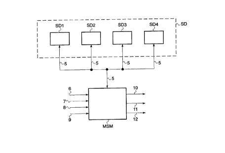
Figure 3 depicts the inputs and outputs of the circuit according to the invention,
indicated as MSM. The circuit, as previously stated, can be assoc;ated with an external
memory SD which, advantageously, co",prises SDRAM (Synchronous Dynamic RAM)
25 elements. In the prerer,ed embodiment of the invention, MSM can co-operate with up to 4
elements, indicated in the Figure as SD1...SD4. By way of example, it is assumed that
the elements can store three pictures each. If SD comprises multiple elements, these are
written and read by MSM one at a time. Line 5 is a schematic represenlalion of the set of
connections between MSM and SD for data exchange and command transmission.
30 The way in which memory SD is organised holds no particular interest for the
purposes of the present invention. To make the description clearer, where necessary
~e~erence shall be made to an exa",~'e in which data in SD are arranged by macro-blocks
and a row is assigned to each macro-block. Depending on the function circuit MSM has to
perform, two writing modes (raster and macro-block) and four reading modes (raster,
35 macro-block reading and extraction, zone extraction) will be possible. Figures 4A...4D
depict a picture portion subjected respectively to raster writing/reading, macro-block
writing/reading, macro-block extraction, zone extraction: it should be stressed that the
2 1 9~55~
portion involved (bounded by the thicker lines in Figures 4B - 4D) is in any case read
sequentially row by row. In case of macro-block and zone extraction (Figures 4C 4D)
where the picture portion to be read extends over lif~erer,l stored macro-blocks the term
'quadrant" shall be used for the set of pixels to be extracted from each of these macro-
5 blocks.
Going back to Figure 3 the inputs to MSM comprise:
- a connection or bus 6 (picture bus) which carries the actual data to be written into the
external memory or to be transferred to the output after macro-block/block format
conversion or vice versa; bus 6 is advantageously a 10-bit bus, since as previously
10 stated the device can be used immediately upstream or downstream of the transform
(anti-transform) computation circuits which require 10 significant bits;
- a connection or bus 7 which carries the data synchronism signals;
- a connection or bus 8 (information bus) which carries the parameters required for
processing incoming and outgoing samples when device MSM operates in macro-
15 block mode; the parameters of interest shall be examined in the detailed description ofthe structure of device MSM;
- a connection or bus 9 for synchronism signals concerning parameter extraction from
bus 8.
The organisation of the information on bus 8 and of the related synchronism signals
20 on bus 9 is described in patent application PCT/GB 95 01433.
MSM outputs are: two connections 10, 11 for data (8-bit connections) and a
connection 12 for synchronism signals. The two connections for the outgoing data are
necessary in the case of zone extraction to allow e-"ission of all data in the available
time and in the case of 1 0-bit output: in that case one of the connections carries the eight
25 least significant bits and the other one the two most sig"ificanl bits.
With regard to synchronism by way of non-limiting example reference will be madeto a clock frequency of 18 MHz on the picture bus and on the information bus and to a
frequency of 36 MHz for reading/writing in SD. The main synchronism signals of interest
for an understanding of the invention are: the picture syncl,runis,,, signal (whose period is
30 equal to the duration of the 36x45 or 30x45 macro-blocks) and the macro-blocksynchronis;" signal (whose period is equal to 420 pulses of the 18 MHz clock signal)
when the circuit operates in macro-block mode; the frame synchronism and line
sy,,chrunis;n signals when input or output signals are in raster format. Valid data signals
are also provided.
3 5 It should be stressed that in the macro-block time the data of a macro-block are to
be written in SD whereas data of two macro-blocks must be read in certain operating
modes. To allow this the macro-block period is divided into three parts: the first one
- - 21 98555
whose duration is about 100 pulses of the 18 MHz clock signal, is destined to writing,
whilst the other two parts, identical to each other, are destined each to reading a macro-
block. That partition of the macro-block time is shown in Fig. 7B, where the writing and
reading intervals are denoted WR and RD, respectively. The longer time interval assigned
5 to reading a macro-block stems from the greater complexity of reading operations, as it
will be better explained hereL~a~ler.
Figure 5 shows that in circuit MSM connections 6, 7 lead to a first internal buffer
memory, sche"ldlically represented with its control units by block MT1. Outputs from MT1
cGi"pnse a connection 5a (belonging to line 5 shown in Figure 3), which carries data and
10 some control signals, to be seen further on, to extemal memory SD, and a pair of
conne~ions 50, 51 which, when the device operates without using the external memory,
supF'.es an output interface SU with the data and synchronism signals to be transferred
on connections 10 - 12.
Connections 8 and 9, on the other hand, lead to a decoder DIB which, at the
15 appropriale instants, extracts paramel6rs of interest for the specific application from the
stream present on the information bus and feeds them to MT1 and/or to units ISS, CM.
The latter units, in certain applications of the device and in co-operation with a conlr."Er
CME of the external memory, provide for external memory addlessing during writing (ISS)
or reading (CM) and for motion compensation (CM).
2 o Data read from the external memory are received by device MSM through a bus 5b
(which also belongs to line 5 shown in Figure 3) which leads to an interpolation unit IHV.
That unit sends the data to a second internal buffer memory, schematically represented
with its control units by block MT2, and then to output inter~ace SU.
Circuit MSM also comprises a conventional ,,,icroplucessor interface IU, which
25 allows connection with an external controller, not shown, which provides for controlling,
supervising and setting up the functions to be performed. Control of communication
between circuit MSM and the external controller occurs by means of signals present on a
connection 14. Interface IU is also associated with a configuration register RC, which is
written by the external conlrc"~r through a connection 13 and provides all remaining units
30 of the device, through bus 15, with information concerning the function to be performed.
Instead of receiving the parameters of interest from information bus 8, device MSM
could receive such parameters from the external conl,~l'cr, through connection 13 which
also leads to unit DIB, to allow that kind of operation. In any case, it is the task of the
external controller to provide the parameters required for infon"~lion reception/emission
35 in raster format. The loading of the parameters provided by the external conl,c"er into
DIB is cor,l,~l'ed by IU, through connection 30.
The device according to the invention could also be an autonomous device, which
2! ~8555
does not employ an external controller. In that case connection 14 is wired so that signals
present on it have a pre-set configuration, not used for the signals generated by the
cor,l.~ller. Connection 13 also is wired so that signals on it represent appr~priale
configuration parameters. Interface IU, when it recognises the special configuration on
5 connection 14, will cause, through connection 31, in~o""ation wired on connection 13 to
be loaded into RC.
For the sake of simplicity, Figure 5 and the more detailed Figures which follow do
not show clock signals, reset signals and in general all those signals which are not
necessAry for an understanding of the invention. Note that the syl,chr.,nisalion of
0 operdlions performed by the various units of the device is handled in a distributed fashion,
by appropriate time counters present in the units themselves.
The functions performed by the various units of MSM shall now be examined in
greater detail.
Buffer memory MT1 comprises two elements in ping-pong arrangement, alternating
15 in writing and reading operations at macro-block frequency. The elements are structured
in such a way as to store pixel pairs. During the reading phase, blocks of 8 pixel pairs will
be transferred to the external memory or to the output. The structure of MT1 shall be
described in greater detail with reference to Figure 6.
Unit DIB receives the parameters according to which data incoming to device MSM
20 (writing) and respectively data outgoing from the device (reading), are to be processed,
and extracts them according to the synchronism signals present on connection 9. The
parameters are organised in nibbles (half-bytes) arranged in a pre-set order in the
stream, so that their meaning can immediately be deduced from the order in which they
reach DIB. Unit DIB therefore essentially comprises a nibble counter and two groups of
25 registers, to store the parameters for processing incoming and outgoing data
respectively. Each register group in turn comprises two sets of registers which make
available to downstream units the whole of the information concerning the current picture
and respectively the information concerning the current macro-block.
In particular, in the writing phase, circuit DIB must extract, at picture frequency,
30 information about: type of encoded picture (I, P, B); picture structure ("frame" or "field"
and, in the latter case, lower or upper field); external memory element and position, inside
the element, where the picture is to be written.
I"for",dlion at macro-block frequency of interest for writing is the type of lrtu~sfonll
and, for macro-block/block conversion and vice versa, the block format (progressive/
35 interlaced).
For reading, the information required at picture frequency is the same as for writing.
At macro-block frequency, on the other hand, DIB extracts motion compensation
21 98555
parameters, in particular:
- compensalion type fforward, backward, both or neither);
- prediction mode: more specifically, for a "frame" type of picture, prediction can be:
"framen, concerning the complete macro-block and requiring a single motion vector;
5 "fieldn, pertaining to the two fields separately and requiring two motion vectors; "dual
prime~, consisting of a double field prediction and of a crossecl combination (lower-
upper fields) of the two predictions to yield the predicted macro-block, and requiring
four motion vectors. For the field picture, prediction can be: "field" (wholly analogous to
the "frame" prediction mentioned above); 1 6x8, which concer"s the upper or lower half
10 of a macro-block and requires two motion vectors; Udual primen, cons;~ti"g of a double
field prediction and of a co",t.,ation of the results and also requiring two motion
vectors;
- the vertical selection of the field, which indicates which field the motion vector is to be
applied to;
15 - motion vectors.
Unit ISS is a finite state machine which, when data need to be written in macro-block format in SD, generates writing addlesses for SD according to the parameters
provided by decoder DIB (wires 8a) and to signals MBC, MBS which are provided by MT1
through connection 16 and represent the co-ordinates of a column and of a stripe of
20 macro-blocks in the picture. Addresses are sent to CME through connection 18. Clearly,
the address generation law depends on data arrangement in SD: knowing that
arrangement, the person skilled in the art has no problem in designing logic network ISS.
Unit CM generates and sends to external memory conl,~"~r CME address signals
and commands for reading in SD (Figure 3) in one of the three macro-block format25 reading modes (macro-block reading and extraction, zone extraction). For that purpose
CM receives reading parameters from DIB, through wires 8b; moreover, through a
connection 20, CM will exchange a certain number of signals with CME and, through a
connection 21, it receives timing signals from MT2. Note that when data arrive at or have
to be emitted from MSM in raster format, circuit CM does not intervene and CME is
3 0 entirely tasked with add, ess;"g. The structure of CM is shown in greater detail in Figure 7.
Controller CME is tasked with driving the external memory addressing and controlsignals, presented respectively on connections 5c, 5d, in the different writing and reading
modes described above. In case of raster writingtreading, CME generates the ad.l~sses
autonomously, whilst in the other cases it receives the addresses from ISS, CM. The
3 5 structure of CME shall be described in greater detail with reference to Figure 8.
Buffer memory MT2 co"~prises two pairs of elements in ping-pong arrangement,
alternating in writing and reading operations at macro-block frequency. A pair of elements
21 98555
is needed to store data read from SD (Figure 3), in place of a single element as in MT1,
as certain motion prediction and compensation modes require a combination of pixels of
picture pairs to be performed and, in zone extraction, pixels from two zones are to be
emitted. Data to be written arrive in pairs from interpolator IHV and are written
5 sequentially (in frame or field mode). Writing and reading are progressive, in frame or
field mode. Reading is slaved, in terms of timing, to reading from SD (Figure 3). If both
eleh,erll~ in a pair are to be used, they are written one after the other and read
concurrently.
Given these indications, designing MT2 does not present any problems to the
10 skilled in the art.
Pixels are transferred from unit MT2 to output interface SU together with valid data
signals, present on a wire 52. SU performs any required pixel combination or emits the
data as they are read, if no combination is required; moreover it associates the data with
the synchronism and valid data signals necessary in order the utilisation devices can
15 recover the data correctly. With regard to valid data signals, either the ones provided by
MT1 on a wire 51 or the ones provided by MT2 on a wire 52 shall be used, depending on
the ~pp'ir,~tions of device MSM. SU is described in greater detail with reference to Figure
9.
Unit IHV is to create a new macro-block whose pixels are the average between
20 adjacent pixels in the macro-block read from SD (interpolation). Information needed to
perform that function is represented by signals H_INT, V_INT which, when active, request
interpolation along the horizontal and the vertical axis, respectively, of the macro-block.
Those signals are provided through connection 22 by motion compensation unit CM,depending on the content of the motion vector, whose resolution is half pixel. Processed
25 data are transferred to unit MT2 through a connection 23. Unit IHV comprises a control
state machine and an operating unit. The first one operates on the basis of signals
H_INT, V_INT and of an additional signal FS_BYTE, also generated by CM, which
indicates whether, for each pixel pair, the first pixel is to be processed or discarded. The
operating unit, instead, is tasked with computing the required averages (hence
3 0 performing additions and d;~ ons). Unit IHV is transparent to data if device MSM is used
for conversion into raster format; if circuit MSM is used for zone extraction, unit IHV only
discards the first pixel, if necessary.
In Figure 6A, RAM1, RAM2 indicate the two elements of the first buffer memory
MT1. Such elements receive addless;ng and control signals for writing and reading
3 5 respectively from two finite state machines WM1, RM1, by means of a multiplexer MX1.
Through MX1, the memory element which is being written receives from WM1 also the
data arriving at MSM (Figure 3) through bus 6, and the element which is being read
- 21 98555
transfers the data read to RM1, which forwards them on bus 5a or 50. WM1 sends to
multiplexer MX1 addresses and data (through connections 60, 61), signals WE1, WE2
enabling writing/reading into/from either element, and signals ME1, ME2 timing the
loading of an address or a datum into the memory. The outputs of WM1 on which these
5 control signals are present are represented schematically in the whole by conne~:tion 62.
The sequence of e",ission of writing commands, addlesses and data is the sequence
typical for any memory and therefore a more dePi'~d desc,i,ution is not required. RM1
instead generates reading addresses, sent to MX1 through a connection 63.
Outputs 61-i, 62-i, 64-i (i = 1,2) from MX1 indicate the connections transferring to
10 RAM1 and RAM2 the data to be written, the control signals and the add~esses present on
connections 60, 63: clearly, at each macro-block cycle the connections between inputs
60, 63 and outputs 61-1, 62-1, 64-1 and 61-2, 62-2, 64-2 will be reversed.
Outputs 67, 68 of RAM1, RAM2 (which are 20-bit buses, since data transfer
towards the exter"al memory involves a pixel pair each time) are brought back to the
15 inputs of multiplexer MX1 which, depending on which of the two memories is being read,
connects output 67 or 68 to data output connection 69 (also at 20 bits). This connection
leads to an input of RM1 which, for the apFI--~tions entailing the use of the external
memory, converts the output format from 20 to 16 bits and emits the data on a first group
of wires of connection 5a.1f the circuit app'i~Ation does not require access to the external
20 memory, RM1 presents the data on bus 50 at 10 bit for transfer to SU (which transfer
therefore occurs again by individual pixels, and not in pairs) and generates, on connection
51, synchronism signals for outgoing data (in particular, a valid data signal).
Logic network WM1 makes pixels to be written into RAM1, RAM2 in the order they
arrive and, as stated above, it provides RAM1 or RAM2 with two pixels at a time. When
25 data incoming over connection 6 are in block or macro-block format, during the macro-
block time WM1 must command writing of 384 pixels (256 for luminance and 128 forchrominance) into RAM1 or RAM2, whilst in case of data in raster format the number of
pixels to be written varies from a minimum value to 420, depending on the relative
position of the line synchronism signals and of the blanking periods (during which no valid
30 data are present) with respect to the macro-block period, as can be seen in Figure 6B.
There, MB, LN indicate respectively the macro-block and line syncllronis", signal, BE, RE
indicate valid data signals (for macro-block and raster format, respectively) and 6(MB)
and 6(R) indicate the data present on bus 6 in the two cases. Note that the data are
assumed to be valid when signals BE, RE are at low logic level. As can be seen, in the
35 case of raster format, during the first macro-block period shown, x+y pixels of two
different lines will be written into the memory, given the presence of a blanking period (RE
at high logic level), whilst during the second period 420 pixels of a same line will be
2 1 98555
written; there is again a blanking interval during the third macro-block period, and
therefore z pixels of a line and a certain number of pixels of another line will be written.
This shall have to be taken into account in the course of reading, as will be better seen
further on.
5 For its operation, WM1 needs the following signals:
- a master clock signal which is represented by the macro-block synchronis." signal
present on connection 9;
- picture and macro-block sy"chroni~,l" signals WP, WMB and a valid data signal WBE
(in case of input in macro-block or block format), or alternatively, in case of raster
10 scan operation, field and line sy"chronis", signals F, LN and a respective valid data
signal RE; these signals are present on connection 7; for raster operation, WM1 is also
provided with a signal FST_FIELD (derived for instance from the parameters read by
DIB, Figure 5) which indicates that the incoming field is the first or second one and
which is used by a line counter (within WM1) to determine the initial count value;
15 - the parameter indicating upper or lower field, provided by decoder DIB through wires
8a;
- a signal (STILL_READING) indicating that reading is in progress provided by RM1
through a wire 65 to prevent the unwanted switching between the functions of RAM1,
RAM2.
20 In addition to the signals already seen, WM1 emits:
- on wires 17a of connection 17, value CNT LN of the line number count, destined to
external memory conlr.l'~r CME which uses it for addressing in case of raster writing;
- on a group of wires 66 connected to RM1: a signal RD indicating the beginning of the
writing operation (regardless of the operation mode) and allowing logic network RM1 to
25 be set up for subsequent reading; in case of raster operation, the pixel count
(NWRITE), the pixel-per-line count (NWRITE_LN) and the line change signal (LN).
This information is required in order to take into account some particular situations,
which will be seen in connection with RM1.
In correspondence with the macro-block syl,chloni~,.ll pulse, WM1 also extracts
3 0 from the data stream information which precede the pixels of the picture, in particular:
- a picture structure indication, which can have a particular configuration that indicates
whether the data which follow refer to a repeated field ("dormant fieldn). Field repetition
is necessary in order to transfer data correctly from a system operating at 50 Hz to one
operating at 60 Hz or vice versa. In correspondence with that i"~or",~lion, writing into
35 the memory is disabled;
- word pair MBC and MBS, which are transferred to CM through wires 16a of connection
16 and which are present only in case of operation in macro-block format.
2~ ~8555
14
Logic network RM1 has to control a sequential reading from RAM1 or RAM2 if the
data are to be sent to the external memory, since in that case it is up to ISS and/or CME
(Figure 5) to provide the appropriate ad.l~essi"g; if on the contrary the data are to be
transferred to output bus or buses 10, 11, reading takes place in a manner depending on
5 the required format.
RM1 must receive, in addition to the master clock signal and to the signals coming
from WM1, the picture synchronism signal for reading and, for format conversion from
macro-block to block or vice versa, the parameter that indicates the type of block. This
information is provided by DIB (Figure 5) through wires 8a. RM1 provides CME, through
10 wires 17b of connection 17, with a signal EN_WR enabling writing into the e,cler,,al
memory and, in case of raster operation, with a start line signal (START_LINE).
Moreover, in case of macro-block format, RM1 provides ISS, through wires 16b of
connection 16, with a signal NRAS requesting generation of a new row address for the
external memory.
If the signals on bus 6 are in raster format, data transfer from RAM1 or RAM2 to the
external memory requires some expedients. As said, the external memory must receive
groups of 8 pixel pairs (i.e. the equivalent of one row of a macro-block), and hence 8 pixel
pairs are to be read each time from RAM1 or RAM2. 1 lol/cvcr, as has been seen in
Figure 6B, the macro-block synchronism signal could arrive while the data of a same line
20 are being written into RAM1 or RAM2: thus, the consequent switching of the buffer
element involved in writing may take place before the loading of a group of 8 pixel pairs
has been completed. Moreover, the overall number of pixel pairs loaded might not be a
multiple of 8. Therefore it may happen that data which are to be written at a same
address of the external memory or which are involved in a same transfer operation
25 towards that memory, are to be read in part from RAM1 and in part from RAM2. The 8
pixel pairs read from RAM1 or RAM2 during a certain phase can therefore contain some
non significant data: under these conditions logic network RM1 generates a signal DMQ,
that is sent directly to SD through additional wires of connection 5a to mask the non
siy"i~icant data. Addilionally, data belonging to two di~er6nl lines may have been written
30 in a same element, and this also needs to be siy,l~'led to the extemal memory. This is the
purpose of the START_LINE signal.
As can be seen in Figure 7A, unit CM comprises: a combinatory logic network CSP
computing the initial address of the macro-block or zone to be read or extracted; a bank
of registers REG for temporarily storing and processing the initial address; a control logic
35 networkARB.
Col "~ .. ,at~,l y network CSP computes and sends to registers REG, through
connections 70, 71, the row and column addlesses of the first pixel of a macro-block of
21 9~55;~
the reference picture stored in SD, by applying if necessary one or more motion vectors,
depending on the function required of device MSM (which function is indicated by the
configuration signals present on connection 15). For that purpose CSP \,vill receive the
ap,cr~,priate parameters from DIB (Figure 5) through connection 8b and will receive from
s logic network ARB, through a connection 72, information on the involved vector and on
whether the pixels to be extracted are chrominance or luminance pixels. In that regard, it
is reminded that in case of macro-block extraction, depending on the motion
compensaliol) and prediction modes, it may be necessary to extract data of two macro-
blocks and to apply two motion vectors to each macro-block, both for luminance and for
10 chro",il ,ance. Therefore, for a single reading from SD (Fig. 3), CSP may have to compute
eight initial addlesses. This situation is shown in Figure 7B, which shows the time
arrangement of reading operation in SD (interval RD) in case of bi-directional
compensation: MB is the macro-block synci1roni~", signal, TB_TF is a signal identifying
the beginning i"sldnts of the two reading operations of each macro-block cycle, BW and
15 FW indicate the periods destined to reading the future and the past reference pictures,
respectively, BWi and TWi (i = 1, 2) indicate the ~pp'i~tion of the two motion vectors and
Y, C indicate the reading of luminance and chrominance pixels, respectively. The initial
address therefore must be computed for every Y and every C.
Register bank REG comprises a number of registers linked with the maximum
20 number of quadrants in the picture portion to be read (thus up to 12 quadrants, as it can
be required for zone extraction). The involved register, selected by ARB through a signal
LOAD, loads the row and column address provided by CSP and increments the columnaddress while reading the pixels of a quadrant, on command from logic network ARB
(signal INCR_COL). On command from ARB (signal COL_ROW, which selects the
25 register from which the address is to be taken) the updated address is presented on a
connection 19 for transfer to CME.
REG also generates, on connection 22, the signals required for the operation of
interpolation unit IHV (signals H_INT, V_INT, FS_BYTE already examined) and signals
necess~ry for the operation of CME. The latter are essentially:
30 - a signal RDCOUNT which, in case of macro-block or zone extraction, indicates how
many pixel pairs are to be read from the first quadrant to be extracted: from that
information clearly enables controller CME to obtain information on the number of
pixels of the other quadrants;
- a signal NLINES which, again in case of macro-block or zone extraction,
35 commu" -~tes to CME the number of lines to be read within a quadrant; the value of
NLINES is progressively updated by ARB (signal DECR_NLINES) as a line is read;
depending on reading progress, ARB can provide CSP with the information about the
21 98555
16
motion vector and the chrominance/luminance alternation;
- signal FS_BYTE, already rliscussed.
Logic ARB generates signals LOAD, INCR_COL, COL_ROW described above by
exploiting, in addition to configuration information, also signal TB_TF, which is sur)F'i~d by
5 MT2 through a connection 21, and the requests for new ad.l~esses RAS_REQ and
CAS_REQ coming from CME (wires 20c). ARB also generates the read-enable signal
EN_RD and an addilional signal LAST_ADD which is active in case of macro-block
extraction and communicates that the first two quadrants have been read. These two
signals are sent to CME (wires 20b).
10 As can be seen in Figure 8, conlr.ller CME con,plises
- a first finite state machine WRS, destined to provide SD (Figure 3) with add~esses and
commands for reading and writing operations;
- a second finite state machine GDV, destined to generate a signal DQ_VALID
indicating a significant data in the reading phase (thus, a signal analogous to signal
15 DMQ generated by RM1, Figure 6);
- a combinatory network CIR for computing addresses for SD in case of raster
writing/reading.
A multiplexing system MX2, depending on the functions the device is to carry out,
transfers on connections 80, 81 connected to WRS either the writing and reading
20 addlesses emitted by CIR on outputs 82, 83, or those generated by ISS or CM (Figure 5)
and present on connections 18, 19.
For its operation, logic network WRS receives the write-enable or read-enable
signals EN_WR, EN_RD from MT1 or CM (Figure 5), and receives from CIR a pair of
configuration signals (MB_RASTER, ZONE) whose combination allows programming the25 different modes for ~ccescing SD for writing or reading. In case of zone extraction, WRS
also receives an additional configuration signal bearing the zone size information (SIZE).
That information is also provided to GDV. The signals commanding evolution of the
operation of CME for the different operating modes shall be seen below.
Combinatory logic CIR essentially performs the same functions as blocks CSP and
30 REG shown in Figure 7. CIR computes, separately for chrominance and luminance, the
row and column address for SD (Figure 3) where the first pixel of a given line is to be
written or read: that computation is performed on the basis of line number countCNT_LN, provided by block WM1 (Figure 6) through wires 17a, and of an even/odd line
indication derived from that count. For its operations, CIR also ~eceives a synchr~nis",
35 signal FOUT, provided by control units in MT2 (Fig. 5) through wire 25 and indicating
whether the pixel belongs to the first or the second field, and signal START_LINE, which
signals the line change. The determination of the initial address and the subsequent
21 98555
updating take place according to an algorithm which takes into account how data are
arranged in the external memory. Such algorithm is not of interest for the invention. In any
case, for a given arrangement, the person skilled in the art has no problems in
detemmining the address generation law.
For writing/reading a macro-block it is necessary to take into account that all pixels
of a macro-block are stored in the same row in external memory SD: therefore unit WRS,
every 8 pixel pairs, will need only a new column address, which is requested from CM by
means of a signal CAS_REQ (present on one of wires 1 9b).
For macro-block or zone extraction (see also Figures 4C, 4D), forming each row of
10 the extracted macro-block or zone requires addlessi"g a different macro-block at each
passage from one quadrant to another; moreover, once one row has been completed, it
is possible either to return to a macro-block previously addressed or to move on to a new
macro-block. Under these conditions WRS shall also have to generate row address
requests (RAS_REQ) towards CM (Fig. 5). SDRAM memories are programmable for
15 rapid operation when that type of access is required. Advantageously, in case of macro-
block extraction only the column address request is sent when the new row of the macro-
block being extracted is formed with data of a quadrant read previously, whereas both the
row and the column address requests are sent when moving to a new quadrant; in case
of zone extraction, on the other hand, both addlesses will be requested at each quadrant
20 change, be it new or not. In order rapidly to prepare the new address requests, logic
WRS receives from CM signals RDCOUNT and NLINES, already examined.
In that type of operation, WRS also sends to GDV, through a connection 85, signals
(CNT_LEFT, CNT_CENTER, CNT_RIGHT for zone extraction, and CAS1, CAS2 for
macro-block extraction) informing about the quadrant being read. On the basis of that
25 i,lfor",ation or of a valid data signal in raster reading (DQRAST_VALID) provided by CIR
through a connection 84, GDV sends masking signal DQ_VALID towards the external
memory. This signal, in case of zone extraction, may be activated and de-activated when
beginning and ending reading data of one row of the individual quadrants.
Figure 9 represents output stage SU with its connections to the four memory
3 o elements RAM3 - RAM6 of MT2. It is assumed that: if the operating mode entails writing
in two memory elements within the macro-block time, the element pair involved in the
operation comprises RAM3 and RAM5 or RAM4 and RAM6, respectively; if a single
memory element is sufficient, RAM3 or RAM4 is used; if the data are to be transferred on
a single output bus, bus 10 is used.
3 5 The output stage must provide:
- a co"~ lion of the pixels stored in the two memory elements when a bi-directional
motion compensation is performed;
21 98555
18
- the pixels read from a memory element, if the circuit has to emit data in raster format
or if a macro-block reading was perfommed;
- on the two buses 10 and 11, the data read in parallel from the two memory elements in
case of zone extraction or respectively the least significant byte and the two more
5 Si!JI ,ificant bits of pixels requiring 10 bits.
For that purpose, outputs 24a, 24b and respectively 24c, 24d of RAM3 - RAM6 are
connected to the inputs of a pair of multiplexers MX3, MX4 which select the output of the
element being read and serialise the two bytes read in the memory. Outputs 90, 91 of the
two multiplexers are connected to a combinatory logic COM which, depending on the
10 apF'~ tion, computes an arithmetic average, rounded off by excess, between
homologous pixels read from the two memory elements, or lets data provided by MX3
pass unaltered. Output 92 of COM is connected to an ad-Jitional multiplexer MX5
connecting bus 10 either to that output or to the wires of bus 50 on which are present the
8 least significant bits of the data coming from MT1. MX5 has an additional input 93
15 which, regardless of the a,vp'.~tion, allows transmitting, in correspondence with the
macro-block synchronism signal, the 3 bytes of the macro-block label, i.e. the time stamp
and the row and stripe indications MBC, MBS seen in connection with MT1. This label is
obtained from the information provided by DIB through wires 8b and is presented at the
output of a register RIB. Output 91 of MX4 is instead connected to a multiplexer MX6
20 which, depending on the ~p,~ tion, connects bus 11 either to output 91 of MX4 or to the
wires of bus 50 on which the two most significant bits of the data coming from MT1 are
present .
An additional multiplexer, not shown, emits (e.g. on bus 10) either of the valid data
signals described previously.
25 Output interface SU also comprises a finite state machine SY for managing
synchrol,;s." signals in the phases in which the device reads data from SD (Fig.3). SY is
essentially tasked with re-transl"illi"g towards the outside, with a s~;t~hl~ delay, a pair of
sy~ l~;l ,ronisl" signals RP_F, RMB_LN for the reading phase, which it receives through bus
9. These two signals have a dfflerent meaning and differently handled depending on
30 whether the device has to emit signals in macro-block or raster scan format. In the first
case, the two signals represent the picture and the macro-block synchronisl "
,respectively, and are delayed by a first fixed time, which in the preferred embodiment
essentially corresponds to the duration of one macro-block (or more exactly to 421 pulses
of the 18 MHz clock signal, i.e. one pulse more than that duration). In the second case
35 these signals represent the field and the line sy-,cl ronis", respectively (the latter with a
period of 1152 or 1144 clock pulses, depending on power supply), and are delayed by a
second time which depends on the relative position between field sy,,chluni~,,,, signal
21 98555
19
RP_F and the master clock signal. That second time varies, in the preferred embodiment,
between the 421 pulses of the 18 MHz clock signal and a time corresponding to the
duration of two macro-blocks. Obviously, SY shall also have to receive in~u""ation about
the functions the device must perform (and thus about the required output format),
5 present on connection 15. For a better u"der~dnding, Figures 10A and 10B depict the
trend of signals RP_F, RMB_LN and of the corresponding output signals P_OUT,
MB_OUT for the macro-block and raster scan output format respectively. T1, T2 indicate
the two delays. The person skilled in the art has no pr~ble "s realising a state machine
performing the aforesaid functions.