Note: Descriptions are shown in the official language in which they were submitted.
~o 96107l23 2 31 9 8 7 i ~ ~ PcT/Gss5/02036
FERROELECTRIC LIQUID CRYSTAL DEVICES
Th~s invention relates to novel ferroelectric liquid crystal devices.
Liquid crystal m~tPri~l~ are widely used in liquid crystal displays such as watches,
c~1r~ tor.s etc. Most displays of this type consist of a thin film of a liquid crystalline
composition sandLwiched in a cell bGlw~G1l two s~ 1Pe, at least one of which is
J~ , and having ~ "1L electrodes on their inner ~ ri~ces On applying a
potential dirrG1G.lce across the electrodes the ~ nm~nt of the molecules of the liquid
crystalline c~ o~ition is altered, res111*ng in an electro-optic effect in the m~tPri~l, which is
exploited by the display. Most often electro-optic effects in the nPm~tic liquid crystal phase
are exploited in such displays. Examples of types of displays include the twisted nt-,m~tir.,
the Free~1Ptir~ 7 effect device, cholesteric memory mode device, cholesteric to nP.m~tic
phase change effect device, dynamic sc~ effect device, two frequency :;witch;l~g effect
device and the '~u~ lwist' effect device. Other types of device include active matrix twisted
nrm~tir.S, pi-cells and ferroelectric liquid crystal devices.
Ferroelectric smectic liquid crystal m~t~ , which can be produced by mixing an achiral
host and a chiral dopant, use the ferroelectric properties of the tilted chiral smectic C, F, G,
H, I, J and K phases. The chiral smectic C phase is deno~ed Sc* with the asterisk denoting
chirality. The Sc* phase is PenPr~11y considered to be the most useful as it is the fastest
~wilc,~ g. Ferroelectric smectic liquid crystal m~tPri~l~ should ideally possess the following
chz..~ l;r.~ low viscosity, controllable ~ul,l~leous polarisation (Ps) and an Sc* phase
that persists over a broad le~ c1~ range, which should include ambient ~ , and
~xhihit~ chemical and photorhpmir~l stability. ~ trri~l~ which possess these çh~offer the prospect of very fast ~wilclfil1g liquid crystal cn..~ ;..g devices. Some applications
of ferroelectric liquid crystals are described by J. S. Patel and J. W. Goodby in Opt. Eng.,
1987, 26, 273.
W 096tO7123 219 ~ 7 1 6 2 PCTtGB95tO2036
In ferroelectric liquid crystal devices the molecules switch between di~~ lignm~nt
directions depending on the polarity of an applied electric field. These devices can be
arranged to exhibit bistability where the molecules tend to remain in one of two states until
~wilcl1ed to the other switched state. Such devices are termed surface stabilised ferroelectric
devices, e.g. as described in US 5061047 and US 4367924 and US 4563059. This bistability
allows the mllltipleY addressing of quite large and complex devices.
One common multiplex display has display clellle~ , i.e. pixels, ~ ged in an x, y matrix
format for the display of e.g. alpha mlm~lic r~ t~,~ The matrix format is provided by
forming the electrodes on one slide as a series of column electrodes, and the electrodes on
the other slide as series of row electrodes. The int~r~ectio~ between each column and row
forrn addressable el~m~nt~ or pixels. Other matrix layouts are known, e.g. seven bar nlml~ri~
displays.
There are many di~lclll multirleY addressing s~hl-m~s. A common feature involves the
appli~ti~ ~ of a voltage, called a strobe voltage to each row or line in sequence.
Coinrj~lPnt~lly with the strobe applied at each row, a~ ;dle voltages, called data voltages,
are applied to all column electrodes. The di~l~nces between the dirr~ s~h~m~s lies in
the shape of the strobe and data voltage waveforms.
Other addressing sr~ s are described in GB-2,146,473-A; GB-2,173,336-A;
GB-2,173,337-A; GB-2,173,629-A; WO 89/05025; Harada et al 1985 S.I.D. Paper 8.4 pp
131-134; Lagerwall et al 1985 I.D.R.C. pp 213-221 and P Maltese et al in Proc 1988
I.D.~.C. p 90-101 Fast Addressing for Ferroelectric LC Display Panels.
96/07123 ~?~ 98 7~ ~ PCT/GB95/02036
The mzlt~riZ~l may be switched between its two states by two strobe pulses of opposite sign,
in conjunction with a data w~vefo~ ;vcly, a blanking pulse may be used to switch
the mzlt~o:rizll into one of its states. Perio~lie~lly the sign of the bl~nkin~ and the strobe pulses
may be ~lt~rn~t~-l to ~ a net d.c. value.
These blanking pulses are normally greater in ~mrlitll~le and length of applie~tit-n than the
strobe pulses so that the m~t('r~ wiL~i~es irrespective of which of the two data w~vcr~ is
applied to any one ;--~ ~e~il;on. Blanking pulses may be applied on a line by line basis ahead
of the strobe, or the whole display may be blanked at one time, or a group of lines may be
.~imlllt~neously blanked.
It is well known in the field of ferroelectric liquid crystal device technology that, in order to
achieve the highest ~- r"~ ...re from devices, it is hll~ulL~lL to use ll~ixLulcs of colll~uu,,ds
which give mZIteriZIl~ pos~ ing the most suitable ferroelectric smectic cll~r~r,tçri~tic~ for
particular types of device.
Devices can be ~ çd for speed by ctn~i~er~ti-n of the rcil,ol.~e time vs pulse voltage
curve. This rrl~tinn~hir may show a ...;..;....~.. in the ~wik,l~ g time (t~nj~) at a p~uL.;ul~
applied voltage (Vmin). At voltages higher or lower than Vmjn the swik;l~illg time is longer
than t~njn. It is well lmrl~r~tood that devices having such a .. ;.. ;........ in their ,c~onse time vs
voltage curve can be mllltiple~r driven at high duty ratio with higher c~ than other
ferroelectric liquid crystal devices. It is ~rt~ d that the said .. ;.. ;... ...in the l~onse time
vs voltage curve should occur at low applied voltage and at short pulse length ~ e-;L~ly to
allow the device to be driven using a low voltage source and fast frame address refresh rate.
WO 96/07123 . ~ ~. PCT/GB9~102036 -
219871 ~ 4
Typical known m~t~riAl~ (where m~teri~ls are a mixLure of compound having suitable liquid
crystal çh~r~tPri~tics) which do not allow such a ",;";..,-.", when inrl~ e~l in a ferroelectric
device include the c~""",l lcially available m~t~riAl~ known as SCE13 and ZLI-3654 (both
supplied by Merck UK Ltd, Poole, Dorset). A device which does show such a ...i~
may be co,~l,u.iLed according to PCT GB 88/01004 and lltili~ing m~tPri~le such as
e.g. co,l",l~ ;ially available SCE8 (Merck UK Ltd). Other ~ ,lcs of prior art mz~tt~ri~l~
are e?~lnrlifietl by PCT/GB/86/00040, PCT/GB87/00441 and UK 2232416B.
There are problems relating to the ",rçl~A~ Al stability of ferroelectric liquid crystal devices.
For çxAmple if a force is applied to a device, e.g. it is dropped or it is subjected to some sort
of impact then the cell may be ~ Age-l usuAlly bec~use the Ali nmlont is adversely ~ffectP~1
~O~ 96/07123 21 9 8 71 6 PCT/GB95/02036
The present invention ovG,~;ullles the above problems relating to the mecll~nic~l stability of
ferroelectric liquid crystal cells by the incGl~o,dlion of a m~ n~:)mer m~tPri~l with a
ferroelectric liquid crystal m~tPri~l
According to this invention a liquid crystal device cn~ .. ;C~c two spaced cell walls each
bearing electrode ~ s and treated on at least one facing surface with an ~lignm,o.nt
layer, a layer of a smectic liquid crystal m~tPrl~l Pn~.klsed bG~W~Gll the cell walls,
,u~* . ;~e(l in that the liquid crystal m~tPri~l contains a small arnount of monnmPr.
Accoldill~, to a further aspect of this invention the liquid crystal m~tPri~l may also contain a
phu~
According to a further aspect of this invention the m- nnmPr may be cured with or without
the ~sc;llce of a field.
The m~t~n~l may be cured in an isotropic or pl~f~al~ly a liquid crystal phase, for ~ ,le a
Sc phase.
Preferably the monomer is present up to an amount of 10w~%, more pl~r~bly up to 5% and
even more pl~;r~ bly the amount of monomer present lies in the range 0.01-2.0%.
Typically the curing involves W curing or heat curing.
On curing the monomeric m~tPri~l may be partly or fully poly..,~ e~l
WO 96/07123 1 9 8 71 ~ PCT/GB95/02036
!~
A furLher aspect of this invention provides for a method of redurinE the ~usc~libility of
ferroelectric liquid crystal cells to impact damage compri~in~ the steps of providing a liquid
crystal device compri~inE two spaced cell walls each bearing electrode structures and treated
on at least one facing surface with an ~ nmPnt layer, a layer of a smectic liquid crystal
m~teri~l Pnr.lc sed bc;Lween the cell walls, rh~r~ctrri~ed by the inclusion of a small amount of
monomer m~tP.ri~l.
For this method the ferroelectric liquid crystal cell may be surface stabilised.
A further aspect of this invention provides for an electro-optic device co.~ç,. ;~ two spaced
cell walls each bearing an electrode structure and treated on at least one facing surface with
an ali~nmpnt layer, a layer of a polymer liqu d crystal m~tçri~l and ferroelectric liquid crystal
m~teri~l enclosed b~tw~en the cell walls rh~r~rt~ri~erl in that the polymer liquid crystal is
prepared by the in-situ polymçri~tion of a mn~ mPr.
The monomp~r may be a liquid crystal monomer.
~96/07123 198 71 ~ rcT/GBg5l02036
The invention will now be described by way of e~mrle only with lcÇc.~.lce to the following
~ LWIIlgS ofwhich:-
Figure 1 ill~ les a liquid crystal device.
Figures 2a and 2b show the before (2a) and after (2b) effects of dropping a ball-bearing
from a height of 2cm onto a liquid crystal cell co~ ;llil.g SCE8 only.
Figures 3a and 3b show the before (3a) and after (3b) effects of dlU~J~)illg a ball-bearing
from a height of 2cm onto a liquid crystal cell co..l;~ g SCE8 and
1% of RLCl before curing.
Figures 4a and 4b show the before (4a) and after (4b) effects of dropping a ball-bealirlg
from a height of 4cm onto a liquid crystal cell co~ ;";~g SCE8 and
1% of RLCl after curing.
Figures 5a and 5b show the before (5a) and after (5b) effects of L~ g a ball-bearing
from a height of 2cm onto a liquid crystal cell COIll;7;ll;l~g SCE8 and
0.5% of RLCl before curing.
Figures 6a and 6b show the before (6a) and after (6b) effects of dropping a ball-bearing
from a height of 2cm onto a liquid crystal cell c~,.l~;.,i,-g SCE8 and
0.5% of RLCl after curing.
Figure 7 shows the after effect of dropping a ball-bearing from a height of 3cm
onto a liquid crystal cell co~ -g SCE8 and 0.5% of RLCl after
curing.
Figure 8 ill~ s a Vmjn, tmjn graph for a th~rm~lly aligned sample of
SCE8 + 0.5% RLCl + a~r~ tely 0.1% Darocur 1173 co~ ~cd
to a sample of SCE8.
2~9~71 ~
WO 96107123 . . . ;'~ PCT/GB9S102036
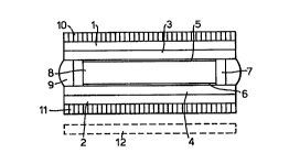
The liquid crystal device con~i~t~ of two Ll~ dlc-lL plates, 1 and 2, for example made from
glass. These plates are coated on their internal face with lldl~dlclll conducting electrodes 3
and 4. An ~lignm~nt layer is introduced onto the internal faces of the cell so that a planar
ol;en~ n of the molecules making up the liquid crystalline m~tPri~l will be al~pn~ n;l~t;ly
parallel to the glass plates 1 and 2. This is done by coating the glass plates 1, 2 co rl~te
with con~lllctin~ electrodes 3, 4 with layers of film 5 and 6 of a suitable polymer, e.g.
polyimide. The electrodes 3, 4 may be formed into row and column electrodes so that the
s~;!;o~ between each column and row form an x, y matrix of addressable elPmtonte or
pixels. Prior to the cOllaLlu~iLion of the cell the films 5, 6 are rubbed with a soft tissue in a
given direction, the l.ll~hlg directions being arranged parallel (same or opposite direction)
UpOll collsL~ Lion of the cell. A spacer 7 e.g. of polymethyl mçth~crylate s~ es the glass
plates 1 and 2 to a suitable ~ t~n~e e.g. 2 microns. Liquid crystal m~tPri~l (typically
inr.lllrlinp at least one type of monomPr and an ilfiLi~Lol) 8 is introduced bGLwGell glass plates
1, 2 by filling the space in bcLwGtll them. This may be done by flow filling the cell using
standard techniques.
The spacer 7 is sealed with an adhesive 9 in a vacuum using an e~ ting technique.
Pola~isers 10, 11 may be arranged in front of and behind the cell. In order to assist the
s~ m~-nt of the liquid crystal m~tPri~l, vatious techniques may be used. One of these
techniques involves thPrm~lly cycling the cell. The m~tPris~l may then be cured with or
without the ~ ,nce of an electric or m~gnPtic field and also with or without the plGsGllce of
a ph~LoilliLidL~Jl. AlLGlll2lLively the liquid crystal m~tPri~l may be ".~ ;"~(1 at the filling
L~AlllJ~d~UI~ and ~UI~S~-Iu~ r cured at that ~
~96/07123 716 PCTIGlil95102036
The curing of the m~teri~l may result in a polymer ll~lv~o-k comrriein~ polymers of varying
molecular weight. There may also be present in small amounts unreacted monr.m,-r.
The device may operate in a tr~nemieeive or reflective mode. In the former, light passing
~rough the device, e.g. from a t~lngeten bulb, is selectively ~ "~,..illed or blocked to form
the desired display. In the reflective mode a mirror (12) is placed behind the second
polariser 11 to reflect ambient light back through the cell and two polarisers. By making the
mirror partly reflecting, the device may be operated both in a ~ x~ ;ve and reflective
mode.
In an ~ ;ve embodiment a single polariser and dye m~t.-ri~l may be combined.
A number of tests were carried out to assess the rÇciet~nce of the device to m~ch~nic~l shock.
In order to test for ~er.l~ shock a hollowed tube was sllep~n~1~cl vertically over a liquid
crystal cell. At regular intervals holes were cut into the tube so that a rod could be il~.t~d
h~ ulll~lly into the tube. A steel ball-bearing, weighing 1.04g, was then ilLs~led into the
top end of the tube so that it came to rest on the hc.li~u~ l rod. The rod could then be
removed and the ball-bearing allowed to drop onto the liquid crystal cell. The energy of
irnpact of the ball-bearing on the liquid crystal cell could then be ~
Having carried out tests of the above type it was then possible to assess the nature of the
damage inflicterl by visual inspection and by ~e!i~e~;lIg some of the :~wilcl~ g c l~ . t~ ;ce
of the liquid crystal cell.
2~9~716 .
WO 96/07123 PCTIGB95/02036
One of ~e m~nomt?rS tested was the commercially available (MERCK, UK) RLCl. Thishas the following formula:
C~2=C~co2 (CH2) 6 ~C2 ~
21 9 ~ 7 ~ 6
WO 96/07123 11 PCTIGB95/02036
Any ferroelectric ~ Lulc is suitable to be used in a device described by the current
invention. Some examples are commercially available (Merck, UK) SCE8 and SCE13.
Any monomer is suitable to be used in a device described by the invention.
FY~mrles of suitable photoiniti~t~rs include Darocurs and Igacurs available from Merck
UK such as Darocur 1173 or 4265 and Igacur 651. There are various UV curables which
are available, some examples are Electrolite c~,~uldLion m~ft~ri~l~ such as ELC 4481
available through LlL~ .ol ics Ltd, Ki~llin~ton, Oxon.
Fx~rnl le 1
SCE13 +5%RLCl +~ O~ t~ly0.1%Darocur 1173.
Fx~m~I le ?
SCE8 + 1% RLCl + d~l~lv~ ely 0.1% Darocur 1173.
F.~m~rle 3
SCE8 + 0.5% RLCl + ~plul~illlately 0.1% Darocur 1173. Therm~lly ~ n~-l
tmin against Vmjn plots were run for e~mrle 3.
For ~ mrle 3, one cell was cured a/ in the ~l~;st;llce of a d.c. field and another cell b/ was
cured without the field. It was only for the cell cured without the presence of a field (3b)
that electro-optic ~wilcl~il~g studies for example tmjn, Vmjn studies could be carried out on.
WO96/07123 219 8 7 ~ t; 12 PCT/GB95/02036
Figures 2-7 illustrate the appearance of liquid crystal cells viewed under a microsco~e
before and after they had been subjected to merh~nir~l shock. Typically cells were
1.5-Z.O~lm thick for these ~ hllcnts, though cells of any suitable thic~n~ee could have
been used.
For the examples contained in Figures 2-7, all of those that were cured were flow filled,
therrn~lly cycled and cured in the Sc phase under a W lamp with no field applied. The
initiator used was Darocur 1173 (~IJro?~illlately 0.1%).
Fx~mples were also tested wherein the m~teri~le were cured in the isotropic state after
flow filling in the isotropic state.