Note: Descriptions are shown in the official language in which they were submitted.
CA 02198836 2000-04-04
OPTICAL WAVELENGTH MULTIPLEXER/DEMULTIPLEXER
This invention relates to an optical wavelength
multiplexer/demultiplexer utilizing an arrayed-waveguide grating
having a wavelength dispersion function, and more particularly to an
optical wavelength multiplexer/demultiplexer which has flatter loss
relative to wavelength characteristics in its passband.
BACKGROUND OF THE INVENTION
Optical communication systems for enhancing information capacity
by transmitting a number of different wavelength optical signals over
an optical f fiber, such as a wavelength division multiplexed (WDM) system,
have been studied. In the WDM system, an optical wavelength
multiplexer/demultiplexer is considered to play a significant role to
multiplex or demultiplex optical signals of different wavelengths
Particularly, one of the most promising optical wavelength
multiplexer/demultiplexers for such use is one which utilizes an
arrayed-waveguide grating, which may increase the number of multiplexed
signals with relatively narrow wavelength spacings. In order to reduce
CA 02198836 1997-10-23
-2-
the variation of insertion losses due to the variation of wavelengths
of light sources, Japanese Published Patent Application No.7-333447 has
proposed an arrayed-waveguide grating that may flatten loss relative
to wavelength characteristics in the vicinity of a center wavelength.
A conventional optical wavelength multiplexer/demultiplexer
comprises an input channel waveguide for receiving a wavelength division
multiplexed signal, a first slab waveguide having an input boundary and
a fan-shaped output boundary, an arrayed-waveguide grating comprising
N channel waveguides which provides a predetermined waveguide length
difference from each other, a second slab waveguide having a fan-shaped
input boundary and an output boundary, a plurality of output channel
waveguides for each receiving a demultiplexed optical signal having a
desired wavelength. The input channel waveguide is connected to the input
boundary of the first slab waveguide, the fan-shaped output boundary
of which is connected to the input end of the arrayed-waveguide grating.
In the same way, the output end of the arrayed-waveguide grating is
connected to the fan-shaped input boundary of the second slab waveguide,
the output boundary of which is connected to the plurality of output
channel waveguides . All these elements are incorporated in a substrate
CA 02198836 1997-10-23
-3-
to form a single device.
In operation, the wavelength division multiplexed signal, which
is coupled into the input channel waveguide, expands into the first slab
waveguide by diffraction. Then, the expanded signal is distributed to
the channel waveguides of the arrayed-waveguide grating, which are
arranged in such a position that the central axis of each channel
waveguide is uniformly separated by a certain spacing and is
perpendicular to the wavefront of the expanding (fan-shaped) signal.
In this case, distribution of a power of the signal to the arrayed-
waveguide grating, i.e. , distribution of electric field to each channel
waveguide depends on an aperture width of each channel waveguide at the
fan-shaped output boundary of the first slab waveguide. On the other
hand, as each channel waveguide of the arrayed-waveguide has a
predetermined waveguide length difference by adding an extra waveguide
length thereto, each signal, after traveling over each channel waveguide
to the fan-shaped input boundary of the second slab waveguide, has a
predetermined phase difference according to its waveguide length
difference. Since the phase difference depends on the wavelength of the
signal, each signal having a different wavelength is focused on a
CA 02198836 1997-10-23
-4-
different position along the output boundary of the second slab waveguide
due to a lens effect thereof. As a result, selected signals having
different wavelengths from each other are received by the plurality of
output channel waveguides, respectively.
An ideal optical wavelength multiplexer/demultiplexer should
have low and flat loss relative to wavelength characteristics in the
vicinity of each center wavelength. For this purpose, two different
distribution characteristics at the fan-shaped input boundary of the
second slab waveguide may be considered. One is electric field amplitude
distribution along the input boundary, and another is phase difference
distribution there. Ideally, the former may show an amplitude
distribution of repetitive maximum and minimum value, the latter a phase
difference distribution of repetitive "0" and "TC". From this point of
view, the aperture width of each channel waveguide of the arrayed-
waveguide grating at the fan-shaped output boundary of the first slab
waveguide, and the extra waveguide length of each channel waveguide are
designed.
In the conventional optical wavelength
multiplexer/demultiplexer, however, there is a disadvantage in thatits
CA 02198836 2000-04-04
-5-
loss is still high in the vicinity of each center wavelength because
of a relatively larger amount of leaked lights at the fan-shaped output
boundary of the first slab waveguide. In addition to that, there is
another disadvantage in that the leaked lights may affect both the
electric field distribution and the phase difference distribution,
which results in a deterioration of cross-talk characteristics.
Therefore, it is still difficult to obtain flatter loss relative to
wavelength characteristics.
Accordingly, it is an obj ect of the invention to provide an optical
wavelength multiplexer/demultiplexer by which its loss in the vicinity
of each center wavelength becomes lower and cross-talk characteristics
are improved.
It is a further object of the invention to provide an optical
wavelength multiplexer/demultiplexer by which flatter loss relative to
wavelength characteristics is obtained.
According to the first feature of the invention, an optical
wavelength multiplexer/demultiplexer incorporated in a substrate,
CA 02198836 1997-10-23
-6-
comprises:
at least one input channel waveguide for receiving a wavelength
division multiplexed signal;
a first slab waveguide having an input boundary and a fan-shaped
output boundary, the input channel waveguide being connected to the input
boundary of the first slab waveguide;
an arrayed-waveguide grating comprising N channel waveguides
which provides a predetermined waveguide length difference from each
other, an input end of the arrayed-waveguide grating being connected
to the fan-shaped output boundary;
a second slab waveguide having a fan-shaped input boundary and
an output boundary, an output end of the arrayed-waveguide grating being
connected to the fan-shaped input boundary of the second slab waveguide;
and
a plurality of output channel waveguides connected to the output
boundary of the second slab waveguide for each receiving an demultiplexed
optical signal having a desired wavelength;
wherein input ends of the N channel waveguides of the
arrayed-waveguide grating are arranged along the fan-shaped output
CA 02198836 1997-10-23
boundary of the first slab waveguide such that an angle 8 between the
central axis of "i"th (i = 1, 2, . . . N) channel waveguide and the symmetric
axis of the fan-shaped output boundary of the first slab waveguide
satisfies the equations in that;
6i + 09i/2
SEg(e)d9 = A x E(i),
8i _ O 6il2
ei - 06i/2 = 6i-1 + 06i-1/2
where Eg( 8 ) is an electric field distribution at the fan-shaped output
boundary of the first slab waveguide, E (i) is a desired electric field
amplitude to be coupled to the "i"th channel waveguide, O 8 i is an angle
made by the central axis perpendicular to a gap on the right side of
the "i"th channel waveguide and that on the left side thereof, and A
is a constant.
According to the second feature of the invention, an optical
wavelength multiplexer/demultiplexer incorporated in a substrate,
comprises:
at least one input channel waveguide for receiving a wavelength
CA 02198836 1997-10-23
_g_
division multiplexed signal;
a first slab waveguide having an input boundary and a fan-shaped
output boundary, the input channel waveguide being connected to the input
boundary of the first slab waveguide;
an arrayed-waveguide grating comprising a plurality of channel
waveguides which provides a predetermined waveguide length difference
from each other, an input end of the arrayed-waveguide grating being
connected to the fan-shaped output boundary;
a second slab waveguide having a fan-shaped input boundary and
an output boundary, an output end of the arrayed-waveguide grating being
connected to the fan-shaped input boundary of the second slab waveguide;
and
a plurality of output channel waveguides connected to the output
boundary of the second slab waveguide for each receiving an demultiplexed
optical signal having a desired wavelength;
wherein each of the plurality of channel waveguides of the
arrayed-waveguide grating is provided with a tapered portion having a
predetermined aperture width at the fan-shaped output boundary of the
first slab waveguide for coupling a predetermined amplitude of electric
CA 02198836 1997-10-23
-9-
field into each said channel waveguide, the plurality of channel
waveguides of the arrayed-waveguide grating are nonuniformly arranged
along the fan-shaped output boundary so that each of adjacent tapered
portions of adjacent channel waveguides is separated by a gap which is
smaller than a predetermined width.
According to the third feature of the invention, an optical
wavelength multiplexer/demultiplexer incorporated in a substrate,
comprises:
at least one input channel waveguide for receiving a wavelength
division multiplexed signal;
a first slab waveguide having an input boundary and a fan-shaped
output boundary, the input channel waveguide being connected to the input
boundary of the first slab waveguide;
an arrayed-waveguide grating comprising a plurality of channel
waveguides which provides a predetermined waveguide length difference
from each other, an input end of the arrayed-waveguide grating being
connected to the fan-shaped output boundary;
a second slab waveguide having a fan-shaped input boundary and
an output boundary, an output end of the arrayed-waveguide grating being
CA 02198836 1997-10-23
-10-
connected to the fan- shaped input boundary of the second slab waveguide;
and
a plurality of output channel waveguides connected to the output
boundary of the second slab waveguide for each receiving an demultiplexed
optical signal having a desired wavelength;
wherein each of the plurality of channel waveguides of the
arrayed-waveguide grating is provided with a tapered portion having a
predetermined aperture width at the fan-shaped output boundary of the
first slab waveguide, the predetermined aperture width of each said
channel waveguide varies in its value repetitively along the fan-shaped
output boundary, the plurality of channel waveguides of the
arrayed-waveguide grating are nonuniformly arranged such that angles
made by the central axes of adj acent channel waveguides vary along the
fan-shaped output boundary so that each gap made by adjacent tapered
portions of the adjacent channel waveguides is smaller than a
predetermined width.
The invention will be explained in more detail in conjunction
CA 02198836 1997-10-23
-11-
with the appended drawings, wherein:
FIG. 1 is a plane view showing a conventional optical wavelength
multiplexer/demultiplexer,
FIG. 2 is a partially plane view, on an enlarged scale, of a portion
of a first slab waveguide in the conventional optical wavelength
multiplexer/demultiplexer shown in FIG. 1,
FIG. 3 is a partially plane view, on a more enlarged scale, showing
the vicinity of an output boundary of the first slab waveguide and input
ends of channel waveguides of arrayed-waveguide grating shown in FIG.
2,
FIG. 4 is a graph showing an example of ideal loss relative to
wavelength characteristics of an ideal optical wavelength
multiplexer/demultiplexer,
FIGS. 5A and 5B are graphs showing distributions of amplitude
and phase difference of signals along an input boundary of second slab
waveguide, respectively, which are calculated based on the ideal loss
relative to wavelength characteristics shown in FIG. 4,
FIGS. 6A and 6B are graphs showing a distribution of aperture
widths of the channel waveguides of the arrayed-waveguide grating at
CA 02198836 1997-10-23
-12-
an output boundary of first slab waveguide, and that of extra waveguide
lengths of the channel waveguides in the conventional optical wavelength
multiplexer/demultiplexer, both of which are relative to the number of
the channel waveguide, respectively,
FIG. 7 is a graph showing an example of actual loss relative to
wavelength characteristics of the conventional
multiplexer/demultiplexer,
FIG. 8 is a plane view showing an optical wavelength
multiplexer/demultiplexer in a preferred embodiment according to the
invention,
FIG. 9 is a partially plane view, on an enlarged scale, of a portion
of a first slab waveguide in the preferred embodiment shown in FIG. 8,
FIG. 10 is a graph showing an example of an angle distribution
relative to the number of the channel waveguide of the arrayed-waveguide
grating, by which the center axes of the channel waveguides are to be
arranged along the output boundary of the first slab waveguide in the
preferred embodiment,
FIGS . 11A and 11B are graphs similar to FIGS . 6A and 6B, but showing
a distribution of the aperture widths of the channel waveguides of the
CA 02198836 1997-10-23
-13-
arrayed-waveguide grating at an output boundary of first slab waveguide,
and that of extra waveguide lengths of the channel waveguides in the
preferred embodiment, respectively, and
FIG. 12 is a graph showing an example of actual loss relative
to wavelength characteristics in the preferred embodiment according to
the invention.
Before explaining an optical wavelength
multiplexer/demultiplexer in the preferred embodiment, the
aforementioned conventional optical wavelength
multiplexer/demultiplexer will be explained in FIGS. 1, 2 and 3.
FIG. 1 shows the conventional optical wavelength
multiplexer/demultiplexer. The optical wavelength
multiplexer/demultiplexer 11 comprises an input channel waveguide 3for
receiving a wavelength division multiplexed signal HI, a first slab
waveguide 14 having an input boundary 14a and a fan-shaped output
boundary 14b, an arrayed-waveguide grating 15 comprising N channel
waveguides 8, which provides a predetermined waveguide length
CA 02198836 1997-10-23
-14-
difference from each other, a second slab waveguide 16 having a
fan-shaped input boundary 16a and an output boundary 16b, N output
channel waveguides 7 for receiving a demultiplexed optical signal H~
having a desired wavelength ~1 1, ~ 2, . . .or ~1 n. The input channel
waveguide 3 is connected to the input boundary 14a of the first slab
waveguide 14, the fan-shaped output boundary 14b of which is connected
to the input end of the arrayed-waveguide grating 15. In the same way,
the output end of the arrayed-waveguide grating 15 is connected to the
fan-shaped input boundary 16a of the second slab waveguide 16, the output
boundary 16b of which is connected to the N output channel waveguides
7 . All these elements are incorporated in a substrate 2 to form a single
optical wavelength multiplexer/demultiplexer 11.
FIG. 2 shows a portion of a first slab waveguide in the
conventional optical wavelength multiplexer/demultiplexer, on an
enlarged scale, wherein like parts are indicated by like reference
numerals as used in FIG. 1. The channel waveguides 8 of the
arrayed-waveguide grating 15 are arranged in such a position that the
central axis of each channel waveguide is uniformly separated by a
constant spacing B from one other and is perpendicular to the fan-shaped
CA 02198836 1997-10-23
-15-
output boundary 14b of the first slab waveguide 14 . The fan-shaped output
boundary 14b has a radius of curvature R, the center of the curvature
is positioned at the center of the input boundary 14a, i . a . , the output
end of the input channel waveguide 3 in FIG. 2, for example. Each of
the channel waveguides 8 of the arrayed-waveguide grating 15 has a
tapered portion 8a by which each of the channel waveguides 8 is connected
to the fan-shaped output boundary 14b of the first slab waveguide 14,
the length of which is L. The input channel waveguide 3, the N output
channel waveguides 7, and the channel waveguides 8 of the arrayed-
waveguide grating 15 have the same waveguide width W, while the tapered
portions 8a of the channel waveguides 8 have the different aperture
widths di (i=1,2,...N), which depend on the position of the channel
waveguides 8 along the fan-shaped output boundary 14b. In addition to
that, each pair of adjacent tapered portions 8 of the channel waveguides
8 make a predetermined width of gap. For example, the gap between the
tapered portion of the "i"th channel waveguide and that of the "i-1"th
channel waveguide is defined as gi.
FIG. 3 shows the vicinity of the fan-shaped output boundary 14b
of the first slab waveguide 14 and input ends of channel waveguides 8
CA 02198836 1997-10-23
-16-
of the arrayed-waveguide grating 15 shown in FIG. 2. The aperture width
di of the tapered portion 8a is defined by the following equation.
di = R x 0 B - 2ti, (1)
ti+ti-1 = gi, and gi = B - (di+di-1)/2, (2)
where R is a radius of curvature of the fan-shaped output boundary of
the first slab waveguide, 0 8 is an angle made by the adjacent center
axes each of which goes through the center of the adjacent pair of channel
waveguides, ti is a gap between one of the adjacent center axes and the
edge of the tapered portion 8a, and B is a constant spacing between the
adjacent channel waveguides (i.e. B = R x O 8).
On the other hand, the "i"th channel waveguide 8 of the
arrayed-waveguide grating 15 has a channel waveguide length defined by
the following equation.
Li = OL x (i-1) + Q(i) + Lc (3)
where O L is a length difference between adjacent channel waveguides
which is necessary to produce wavelength dispersion of a
wavelength-division multiplexedsignallight traveling over the channel
waveguide and couple a desired demultiplexed signal light into the output
channel waveguides, Q (i) is an extra waveguide length to adjust the phase
CA 02198836 1997-10-23
-17-
of the "i"th channel waveguide, Lc is an initial waveguide length of
the first channel waveguide (i.e. i - 1) of the arrayed-waveguide
grating.
In operation, the wavelength division multiplexed signal HI,
which is coupled into the input channel waveguide 3, expands into the
first slab waveguide 14 by diffraction. Then, the expanded signal is
distributed to the channel waveguides 8 of the arrayed-waveguide grating
15, which are arranged in such a position as explained above. In this
case, a distribution of the power of the signal to the arrayed-waveguide
grating 15, i.e., a distribution of electric field to each channel
waveguide 8 depends on the aperture width di of each channel waveguide
8 at the fan- shaped output boundary 14b of the f first slab waveguide 14 .
On the other hand, since each channel waveguide 8 of the arrayed-
waveguide 15 has a predetermined waveguide length difference, each
signal, after traveling over each channel waveguide 8 to the fan-shaped
input boundary 16a of the second slab waveguide 16, has a predetermined
phase difference according to its waveguide length difference. Since
the phase difference depends on the wavelength of the input signal, each
signal having a different wavelength is focused on a different position
CA 02198836 1997-10-23
-18-
along the output boundary 16b of the second slab waveguide 16 due to
a lens effect. As a result, selected output signals H~ having different
wavelengths ~ 1, ~ 2 , . . . ~ n are received by the output channel waveguides
7, respectively.
In the conventional optical wavelength
multiplexer/demultiplexer, since the distributions of electric field
amplitude distribution and phase difference distribution of the input
signal HI at the fan-shaped input boundary 16b of the second slab
waveguide 16 and the loss relative to wavelength characteristics
obtained from the output channel waveguides 7 are related to with each
other by Fourier transformation, these distributions may be determined
by the desired loss relative to wavelength characteristics.
FIG. 4 shows an example of ideal loss relative to wavelength
characteristics of an ideal optical wavelength
multiplexer/demultiplexer. This has flat loss to wavelength
characteristics in the vicinity of each center wavelength (~i-1~
i~ ~i+1~
FIGS. 5A and 5B show examples of an electric field amplitude
distribution and a phase difference distribution of the signal light
CA 02198836 1997-10-23
-19-
at the vicinity of the input boundary 16a of the second slab waveguide
16, which are calculated by the ideal loss relative to wavelength
characteristics, where the horizontal axis shows the number of the
channel waveguides 8 of the arrayed-waveguide grating 15 . In the example,
the number of the channel waveguides 8 is 124 . As shown in FIGS . 5A and
5B, the amplitude has a distribution of repetitive maximum and minimum
value, while the phase has a distribution of repetitive "0" and
". The former characteristics ought to be obtained by adjusting the
aperture width di of each channel waveguide 8 at the fan-shaped output
boundary 14b of the first slab waveguidel4, and the latter be obtained
by adjusting the extra waveguide length Q (i) of each channel waveguide
8. That is to say, it is necessary to adjust the aperture width di and
the extra waveguide length Q(i) of each channel waveguide 8 to obtain
flat loss relative to wavelength characteristics in the vicinity of each
center wavelength.
FIGS . 6A and 6B show examples of distributions of aperture width
di and the extra waveguide length Q(i) of the conventional optical
wavelength multiplexer/demultiplexer, features of which are similar to
the distributions of the electric amplitude and the phase difference
CA 02198836 1997-10-23
-20-
shown in FIGS. 5A and 5B.
If the input signal light HI is ideally distributed into each
channel waveguide 8 of the arrayed-waveguide grating 15, and the phase
of the distributed signal, after traveling over each channel waveguide
8, is ideally adjusted due to the extra waveguide length Q(i) , the ideal
distributions of the amplitude and the phase shown in FIGS. 5A and 5B
may be obtained. As a result, the ideal loss relative to wavelength
characteristics shown in FIG. 4 may be realized. The actual loss relative
to wavelength characteristics of the conventional optical wavelength
multiplexer/demultiplexer, however, are quite different from the ideal
characteristics.
FIG. 7 shows actual loss relative to wavelength characteristics
measured in the conventional optical wavelength
multiplexer/demultiplexer. In this graph, the minimum loss at a center
wavelength of 1555 nm is 8 dB, the 3 dB band width is 0.95 nm, and the
cross-talk is 10 dB. The reason why the actual characteristics in the
conventional optical wavelength multiplexer/demultiplexer differ from
ideal ones will be explained below.
First, in the conventional optical wavelength
CA 02198836 1997-10-23
-21-
multiplexer/demultiplexer shown in FIGS. l, 2, and 3, the channel
waveguides 8 of the arrayed-waveguide grating 15 are uniformly arranged
along the fan-shaped output boundary 14b of the first slab waveguide
by separating each other by a constant spacing B, and the aperture width
di of the tapered portion 8a of each channel waveguide 8 is the only
parameter to be adjusted to obtain an appropriate electric field
amplitude distribution. Therefore, some channel waveguides having a
relatively smaller aperture width di make a larger gaps gi between them.
As a result, a relatively larger amount of leaked lights HL from these
gaps cause higher loss. Second, parts of the leaked lights HL are
recombined with other channel waveguides, which make it difficult to
obtain the aimed electric field amplitude distribution in the channel
waveguide. Moreover, the leaked lights HL cause the fluctuation of phase
of the signal light HI traveling over each channel waveguide, which
results in making cross-talk characteristics worse.
Next, an optical wavelength multiplexer/demultiplexer in the
preferred embodiment will be explained in FIGS. 8 and 9, wherein like
parts are indicated by like reference numerals as used in FIGS. 1, 2
and 3.
CA 02198836 1997-10-23
-22-
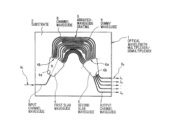
FIG. 8 shows the preferred embodiment of the optical wavelength
multiplexer/demultiplexer according to the invention. The optical
wavelength multiplexer/demultiplexer, which is similar to the
conventional one shown in FIG. 1, comprises an input channel waveguide
3 for receiving a wavelength division multiplexed signal HI, a first
slab waveguide 4 having an input boundary 4a and a fan-shaped output
boundary 4b, an arrayed-waveguide grating 5 comprising N channel
waveguides 8, which provides a predetermined waveguide length
difference from each other, a second slab waveguide 6 having a fan-
shaped input boundary 6a and an output boundary 6b, N output channel
waveguides 7 for each receiving a demultiplexed optical signals H~ having
a desired wavelength ~1, ~2, ...or Vin. The input channel waveguide 3
is connected to the input boundary 4a of the first slab waveguide 4,
the fan-shaped output boundary 4b of which is connected to the input
end of the arrayed-waveguide grating 5. In the same way, the output end
of the arrayed-waveguide grating 5 is connected to the fan-shaped input
boundary 6a of the second slab waveguide 6, the output boundary 6b of
which is connected to N output channel waveguides 7. Moreover, dummy
waveguides 9 are provided between some pairs of adjacent channel
CA 02198836 1997-10-23
-23-
waveguides 8 of the arrayed-waveguide grating 5 so that each of the
waveguides 8 and 9 among the arrayed-waveguide grating 15 is separated
from adjacent waveguides by a substantially equal spacing. All these
elements are incorporated in a substrate 2 to form a single optical
wavelength multiplexer/demultiplexer 1.
FIG. 9 shows a portion of a first slab waveguide in the
conventional optical wavelength multiplexer/demultiplexer, on an
enlarged scale, wherein like parts are indicated by like reference
numerals as used in FIG. 8. The channel waveguides 8 of the
arrayed-waveguide grating 15 are arranged along the fan-shaped output
boundary 4a of the first slab waveguide 4 such that an angle B between
the central axis A~i of "i"th (i = 1, 2, ... N) channel waveguide and
the symmetric axis AS of the fan-shaped output boundary 4 of the first
slab waveguide 4 satisfies the equations in that;
8 i + O B i/2
SEg(6)d6 - A x E(i) , (4)
8i _ 06il2
a i - 0 6 i/2 = a i-1 + 0 a i-1/2 (5)
CA 02198836 1997-10-23
-24-
where Eg( 8 ) is an electric field distribution at the fan-shaped output
boundary of the first slab waveguide, E (i) is a desired electric field
amplitude to be coupled to the "i"th channel waveguide, 0 8 i is an angle
made by the central axis perpendicular to a gap on the right side of
the "i"th channel waveguide and that on the left side thereof, and A
is a constant. In this case, the central axis of each channel waveguide
8 of the arrayed-waveguide grating 5 is perpendicular to the fan- shaped
output boundary 4b of the first slab waveguide 4.
The fan-shaped output boundary 4b has a radius of curvature R,
the center of the curvature is positioned at the center of the input
boundary 4 a, i . a . , the output end of the input channel waveguide 3 , f or
example. Each of the channel waveguides 8 of the arrayed-waveguide
grating 15 has a tapered portion 8a by which each of the channel
waveguides 8 is connected to the fan-shaped output boundary 4b of the
first slab waveguide 4, the length of which is L. The input channel
waveguide 3, the output channel waveguides 7, and the channel waveguides
8 of the arrayed-waveguide grating 5 have the same waveguide width W,
while the tapered portions 8a of the channel waveguides 8 have the
aperture widths di (i=1,2,...N), which are defined by the following
CA 02198836 1997-10-23
-25-
equation.
di = R x 0 B i - g, (6)
where R is a radius of curvature of the fan-shaped output boundary of
the first slab waveguide, g is a gap between adjacent taper portions
of the channel waveguides at the output boundary.
In addition to that, the "i"th channel waveguide 8 of the
arrayed-waveguide grating 5 has a channel waveguide length defined by
the aforementioned equation (3), which is
Li = OL x (i-1) + Q(i) + Lc (3)
where 0 L is a length difference between adjacent channel waveguides,
which is defined by the following equation.
4L = m x ~1/ne (7)
where m is a diffraction degree, ne is an equivalent refractive index
of the channel waveguide.
On the other hand, each output end of the channel waveguides 8
of the arrayed-waveguide grating 5, which are connected to the fan-
shaped input boundary 6a of the second slab waveguide 6, also has a
tapered portion, but the aperture widths are the same. Moreover, the
output ends of the channel waveguides 8 are uniformly arranged along
CA 02198836 2000-04-04
-26-
the fan-shaped input boundary 6a by the same angle spacing.
In the embodiment, the substrate 2 may include, but is not limited
to, a glass substrate, a semiconductor substrate, etc. . Preferably, the
channel waveguides 3, 7, and 8, the dummy waveguides 9, and the first
and second slab waveguides 4 and 6 may be covered by a cladding layer
(not shown) and a buffer layer (not shown), which are formed on the
substrate 2 . These elements maybe made of optically transparent material,
such as, but not limited to, glass, semiconductor, etc..
In operation, the wavelength division multiplexed signal HI,
which is coupled into the input channel waveguide 3, expands into the
first slab waveguide 4 by diffraction. Then, the expanded signal is
distributed to the channel waveguides 8 of the arrayed-waveguide grating
5, which are arranged in such a position as defined by the equations
(4) and (5) .
In this case, as described before, distribution of electric field
to be coupled into each channel waveguide 8 depends on an aperture width
di of each channel waveguide 8 defined by the equation (6). According
to the equation (4) and (5) , the electric field amplitude coupled into
each channel waveguide of the arrayed-waveguide grating 5 (the left side
CA 02198836 1997-10-23
-27-
of the equation (4 ) ) is designed to be proportional to a desired electric
field amplitude (the right side of the equation (4)). As a result, an
ideal distribution of the input signal HI at the fan-shaped output
boundary 6a of the second slab waveguide 6, as shown in FIG. 5A, may
be realized. In the equation (4), the constant A is preferably 0.9 -
1.0 so as to avoid higher insertion loss.
On the other hand, since each channel waveguide 8 of the
arrayed-waveguide 5 has a predetermined waveguide length def fined by the
equations (3) and (7), after the distributed input signal light HI
travels over each channel waveguide 8, an ideal phase difference
distribution at the fan-shaped output boundary 6a of the second slab
waveguide 6, as shown in FIG. 5B, may be realized.
In the second slab waveguide 6, since the phase difference depends
on the wavelength of the signal, each signal having a different
wavelength is focused on a different position along the output boundary
6b of the second slab waveguide 6 due to a lens effect thereof. As a
result, selected output signals HO having different wavelengths ~1,
2,... ~ n are received by the output channel waveguides 7,
respectively.
CA 02198836 1997-10-23
-28-
In the preferred embodiment, the electric field amplitude
distribution and the phase difference distribution of the input signal
HI are desirably controlled. Eventually, the ideal loss relative to
wavelength characteristics having a flat and low loss in the vicinity
of each center wavelength, as shown in FIG. 4, may be obtained.
FIG. 10 shows an example of a calculated distribution of the angle
8 i relative to the number of the channel waveguide 8 of the
arrayed-waveguide grating 5, by which the center axes of the channel
waveguides 8 are to be arranged along the output boundary of the first
slab waveguide in the embodiment.
FIGS. 11A and 11B show examples of a calculated distribution of
the aperture widths di of the channel waveguides 8 of the arrayed-
waveguide grating 5 at the fan-shaped output boundary 6a of first slab
waveguide 6, and that of extra waveguide lengths Q(i) of the channel
waveguides 8 in the preferred embodiment, respectively.
In FIGS. 10, 11A and 11B, R=5000 ~Lm, A=1.01, N=124, W=6~Lm, g=4
I-1.m (g is preferably 2 ~ 6 L~.m, which is suitable for reducing the amount
of leaked lights and sufficiently molding the channel waveguides by
cladding layer (not shown)) are chosen.
CA 02198836 1997-10-23
-29-
As shown in FIG. 10, the angle 8 i distribution is repetitively
changed relatively to the number of the channel waveguide 8 in a
nonuniform fashion. On the other hand, the aperture width di distribution
has a distribution of repetitive maximum and minimum value, as shown
in FIG. 11A. The distribution of the extra waveguide length Q(i), as
shown in FIG. 11B, has a distribution of repetitive increase and decrease,
which corresponds to the phase difference distribution shown in FIG.
5B.
In the preferred embodiment, although the width W of the channel
waveguide 8 of the arrayed-waveguide grating 5 is decided to be 6 ,~
m, the result shown in FIG. 11A may require some channel waveguides whose
aperture widths are so small that adj acent channel waveguides may overlap
with each other. To solve this problem practically, channel waveguides
having a aperture width of less than 4 l~ m are to be omitted.
Referring to FIG. 8 again, the dummy waveguides 9 are provided
between some pairs of adjacent channel waveguides 8 having a relatively
wider spacing so that each of the channel waveguides 8 and the dummy
waveguides 9 among the arrayed-waveguide grating 15, including channel
waveguides 8 having a relatively narrower spacing, is separated from
CA 02198836 1997-10-23
-30-
adjacent waveguides by a substantially equal spacing. The reason will
be explained below.
In the preferred embodiment, the first slab waveguide 4 and the
second slab waveguide 6 are connected by the channel waveguides 8 of
the arrayed-waveguide grating 5, whose lengths satisfy the equation (3) .
On the other hand, the input ends of the channel waveguides 8 are
nonuniformly arranged along the fan-shaped output boundary 4b of the
first slab waveguide 4 in accordance with the equations (4) and (5).
Eventually, the spacing between adjacent channel waveguides 8 varies
over the arrayed-waveguide grating 5. In general, all the waveguides,
including the input channel waveguide 3, the first slab waveguide 4,
the channel waveguides 8 of the arrayed-waveguide grating 5, the second
slab waveguide 6 and the output channel waveguides 7, are made by using
a known etching technique . If the spacings between the adj acent channel
waveguides differ from each other, etching speeds at which the channel
waveguides are formed also differ. Eventually, it may cause a slight
dif f erence of waveguide width among these channel waveguides . As a result,
desired loss relative to wavelength characteristics are not obtained,
because the phase of the signal light HI traveling over the channel
CA 02198836 1997-10-23
-31-
waveguide 8 may shift from the desired phase distribution. According
to the preferred embodiment, each channel waveguide 9 is uniformly etched
to have a substantially equal waveguide width W due to the appropriate
arrangement of the dummy waveguides 9.
Next, a specific example of the optical wavelength
multiplexer/demultiplexer according to the invention will be explained
below.
In order to manufacture the specific example of the optical
wavelength multiplexer/demultiplexer, a Si02 glass waveguide layer
(core layer) containing a Ti02 dopant is deposited on a silica substrate
by an electron beam vapor deposition method. Then the waveguide layer
is etched by using a photoresist pattern to form channel waveguides and
slab waveguides on the substrate. After that, a Si02 cladding layer is
deposited on these waveguides and the substrate by a flame deposition
method, then sintered by an electric furnace to form a transparent glass
layer. The resulting optical wavelength multiplexer/demultiplexer is
designed to have 8 output channel waveguides, each of which has a center
wavelength spacing of 1.6 nm. The parameters of the optical wavelength
multiplexer/demultiplexer are that the diffraction degree m=63, the
CA 02198836 2000-04-04
-32-
equivalent refractive index ne=1.4504, and O L=67.6 a m. Furthermore,
8 i, di and Qi are the same determined by the abovementioned preferred
embodiment, which are shown in FIGS. 10, 11A and 11B.
FIG. 12 shows loss relative to wavelength characteristics of the
specific example of the optical wavelength multiplexer/demultiplexer.
This indicates that the loss at each center wavelength becomes as low
as 5 dB, which is 3 dB lower than the conventional one. And also flatter
loss relative to wavelength characteristics in the vicinity of each
center wavelength is obtained. The 3 dB band width is 1.4 nm, which
is approximately 1.5 times as wide as the conventional one. Moreover,
the cross-talk is 29 d8, which is 19 dB higher than the conventional
one.
As well explained above, the invention provides advantages set
out below.
(1) electric field distribution of the signal light in the
arrayed-waveguide grating is controlled. Then loss relative to
wavelength characteristics having a lower loss, a less cross-talk, and
flatter loss to wavelength characteristics in the vicinity of center
wavelengths are realized.
CA 02198836 2000-04-04
-33-
(2) 3 dB band width is expanded and loss variation due to
wavelength variation is reduced. As a result, the optical communication
system utilizing the optical wavelength multiplexer/demultiplexer is
more tolerant to the variation of a light source wavelength.
Although the invention has been described with respect to specific
embodiment for complete and clear disclosure, the appended claims are
not to be thus limited but are to be construed as embodying all
modification and alternative constructions that may be occur to one
skilled in the art which fairly fall within the basic teaching here is
set forth.