Note: Descriptions are shown in the official language in which they were submitted.
_ - 1 02 1 98 9 63
DIELECTRIC INTEGRATED NONRADIATIVE DIELECTRIC WAVEGUIDE
SUPERCONDUCTING BAND-PASS FILTER APPARATUS
The present invention relates to a dielectric
integrated nonradiative dielectric waveguide
superconducting band-pass filter apparatus employing
nonradiative dielectric~waveguides (hereinafter referred
to as "NRD waveguides").
The following arrangement is disclosed in Japanese
Unexamined Patent Publication No. 3-270401. When an NRD
waveguide such that the upper and lower portions of a
dielectric waveguide shaped, for example, in a
quadrangular prism are interposed and held by a pair of
flat metal plates is formed, the vertical height such that
the dielectric member intersects at right angles to the
direction of the length is a half-wave length or less, and
a brim is extended from one side to the other at the upper
and Lower end portions in order to form an H shaped cross
section,. and a metallic film is formed in close contact at
the outer surfaces of both upper and lower ends of the
dielectric member including the brim portion, thus forming
a dielectric integrated NRD waveguide (hereinafter
b_ - 2 -
021989fi3
referred to as a "first conventional example"). Such a
dielectric integrated NRD waveguide has a feature that
even if vibration and/or impact are received, the metal
section and the dielectric member are not separated from
each other, and stable electrical characteristics can be
obtained.
There has been proposed a dielectric-loaded waveguide
filter or a waveguide-coupled NRD waveguide in which
dielectric resonators at the initial and final stages are
directly coupled to the waveguide. In the arrangement of
such filters, there is a problem in that it is difficult
to adjust the external Q and the resonance frequency
independently from each other. In order to solve this
problem, in Japanese Unexamined Patent Publication No. 63-
59001, a waveguide-coupled NRD guide filter (hereinafter
referred to as a "second conventional example") of a type
in which an NRD guide resonator and a waveguide are
directly coupled is proposed, wherein a buffer dielectric
section is disposed in the connection portion of the NRD
guide resonator and the waveguide, posterior to a
resonator-forming dielectric section of the NRD guide
resonator.
An NRD waveguide is formed by using low dielectric-
constant materials as materials for dielectric waveguides
of an NRD waveguide for use in the first and second
-3-p21g8963
conventional examples. However, if an NRD waveguide is
formed by using high dielectric-constant materials for the
purpose of achieving a smaller size, observation of a
phenomenon in which single mode transmission cannot be
performed has been reported in prior art reference 1
(Soube Shinohara et al., "Specific Transmission
Characteristics of Nonradiative Dielectric Waveguide Using
High Dielectric-Constant Materials", Journal of The
Institute of Electronics, Information and Communication
Engineers of Japan, C-I, Vo1.J73-C-I, No.ll, pp.716-723,
November 1990). The reason why single mode transmission
cannot be performed in the conventional NRD waveguide is
that a very small gap which cannot be avoided in working,
present between the dielectric strip and the metal plate
of the NRD waveguide, narrows the band of single mode
transmission. In order to solve this problem, in the
prior art reference 1, a "trapped insular guide"
(hereinafter referred to as a "third conventional
example") has been proposed as a structural scheme for an
arrangement using high dielectric-constant materials.
However, this third conventional example has a problem in
that the arrangement is complex, and the manufacturing
steps are complex, resulting in a considerable increase in
the manufacturing cost.
- 02 1 98 ~ 63
An object of the present invention is to provide an
NRD waveguide band-pass filter apparatus which solves the
above-described problems, and which is simple in
construction and can be manufactured easily as well as
being formed small in size and light in weight, and which
operates in a single operating mode.
To achieve the above-described object, according to a
first aspect of the present invention, there is provided a
dielectric integrated NRD waveguide superconducting band-
pass filter apparatus which is an NRD waveguide band-pass
filter apparatus having a plurality of NRD waveguide
resonators arrayed in such a way that two adjacent NRD
waveguide resonators are electromagnetically coupled to each
other, the dielectric integrated NRD waveguide
superconducting band-pass filter apparatus comprising: a
rectangular-cylinder-shaped dielectric housing comprising an
upper surface portion and a lower surface portion and a
plurality of dielectric waveguides, in which a plurality of
arrayed rectangular-cylinder-shaped dielectric waveguides
are held by the upper and lower surface portions which are
parallel to each other, and the upper and lower surface
portions, and the plurality of dielectric sections are
formed integrally; a first and a second superconducting
electrode formed on each outer surface of the upper surface
- -5- p219~~63
portion and the lower surface portion, wherein the outer
portion of each dielectric waveguide is formed into a cut-
off area by setting the space between the first and second
superconducting electrodes to one half of the wavelength of
the resonance frequency in a vacuum of the band-pass filter
apparatus.
According to a second aspect of the present invention,
in the dielectric integrated nonradiative dielectric
waveguide superconducting band-pass filter apparatus in
accordance with the first aspect of the present invention,
the dielectric housing further comprises two end surface
portions formed in such a manner as to connect both
longitudinal ends of the upper surface portion and the lower
surface portion, and the band-pass filter apparatus further
comprises a third superconducting electrode or metallic
electrode formed on the outer surfaces of the two end
surface portions.
According to a third aspect of the present invention,
in the dielectric integrated NRD waveguide superconducting
band-pass filter apparatus in accordance with the first or
second aspect of the present invention, the upper surface
portion and the lower surface portion of the dielectric
housing, the connection portion between the two end surface
portions, and the connection portions between each
dielectric waveguide and the upper and lower surface
._ _6- 02198963
portions are chamfered.
According to a fourth aspect of the present
invention, in the dielectric integrated NRD waveguide
superconducting band-pass filter apparatus in accordance
with the first, second or third aspect of the present
invention, the band-pass filter apparatus further
comprises a plane circuit formed on the outer surface of
the upper surface portion.
The above and further objects, aspects-and novel
features of the invention will become more apparent from
the following detailed description when read in connection
with the accompanying drawings.
Fig. 1 is a perspective view illustrating the
exterior of a dielectric integrated NRD waveguide
superconducting band-pass filter apparatus according to a
first embodiment of the present invention;
Fig. 2 is a perspective view illustrating the
exterior of a dielectric integrated NRD waveguide
superconducting band-pass filter apparatus according to a
second embodiment of the present invention;
Fig. 3 is a perspective view illustrating the
exterior of a dielectric integrated NRD waveguide
superconducting band-pass filter apparatus according to a
-~- p2~g~963
first modification of the present invention;
Fig. 4 is a perspective view illustrating the
exterior of a dielectric integrated NRD waveguide
superconducting band-pass filter apparatus according to a
second modification of the present invention;
Fig. 5 is a front view of the band-pass filter
apparatus shown in Fig. 1;
Fig. 6 is a plan view of the band-pass filter
apparatus shown in Fig.~l;
Fig. 7A is a longitudinal sectional view illustrating
the transmission electromagnetic-field distribution of a
TEp1 mode rectangular waveguide in the band-pass filter
apparatus in accordance with the first embodiment, which
view is cut by a plane parallel to the transmission
direction in the rectangular waveguide;
Fig. 7B is a longitudinal sectional view illustrating
the transmission electromagnetic-field distribution of a
TEpl mode rectangular waveguide in the band-pass filter
apparatus in accordance with the first embodiment, which
view is cut by a plane vertical to the transmission
direction in the rectangular waveguide;
Fig. 7C is a longitudinal sectional view illustrating
the transmission electromagnetic-field distribution of a
coaxial waveguide in the band-pass filter apparatus in
accordance with the second embodiment, which view is cut
- 021 9~ X63
by a plane passing the axis parallel to the transmission
direction in the rectangular waveguide;
Fig. 7D is a longitudinal sectional view illustrating
the transmission electromagnetic-field distribution of the
coaxial waveguide in the band-pass filter apparatus in
accordance with the second embodiment, which view is cut
by a plane vertical to the transmission direction in the
rectangular waveguide;
Fig. 8A is a longitudinal sectional view illustrating
the electric-field distribution of the band-pass filter
apparatus in an LSE mode in accordance with the first
embodiment, which view is cut by a plane (A-A' in Fig. 1)
parallel to the transmission direction in the rectangular
waveguide;
Fig. 8B is a longitudinal sectional view illustrating
the magnetic-field distribution of the band-pass filter
apparatus in an LSE mode in accordance with the first
embodiment, which view is cut by a plane (B-B' in Fig. 2)
parallel to the transmission direction in the rectangular
waveguide;
Fig. 9A is a longitudinal sectional view illustrating
the electric-field distribution of the band-pass filter
apparatus in an LSM mode in accordance with the second
embodiment, which view is cut by a plane passing the axis
parallel to the transmission direction in a coaxial
~219~ X63
waveguide;
Fig. 9B is a longitudinal sectional view illustrating
the magnetic-field distribution of the band-pass filter
apparatus in an LSM mode in accordance with the second
embodiment, which view is cut by a plane passing the axis
parallel to the transmission direction in the coaxial
waveguide;
Fig. 10A is a perspective view illustrating the
electric-field distribution of an LSEpl mode transmission
waveguide;
Fig. lOB is a perspective view illustrating the
magnetic-field distribution of the LSEpl mode transmission
waveguide;
Fig. 10C is a perspective view illustrating the
electric-current distribution of the LSEpl mode
transmission waveguide;
Fig. 11A is a perspective view illustrating the
electric-field distribution of an LSEpl mode resonator used
in the first embodiment;
Fig. 11B is a perspective view illustrating the
magnetic-field distribution of the LSEpl mode resonator;
Fig. 11C is a perspective view illustrating the
electric-current distribution of the LSEpl mode resonator;
Fig. 12A is a perspective view illustrating the
electric-field distribution of an LSMpl mode transmission
-so- 0219963
waveguide;
Fig. 12B is a perspective view illustrating the
magnetic-field distribution of the LSMpl mode transmission
waveguide;
Fig. 12C is a perspective view illustrating the
electric-current distribution of the LSMpl mode
transmission waveguide;
Fig. 13A is a perspective view illustrating the
electric-field distribution of an LSMpl mode resonator used
in the second embodiment;
Fig. 13B is a perspective view illustrating the
magnetic-field distribution of the LSMpl mode resonator;
Fig. 13C is a perspective view illustrating the
electric-current distribution of the LSMpl mode resonator;
Fig. 14A is a perspective view illustrating the
electric-field distribution of a TElp mode transmission
waveguide;
Fig. 14B is a perspective view illustrating the
magnetic-field distribution of the TElp mode transmission
waveguide;
Fig. 14C is a perspective view illustrating the
electric-current distribution of the TElp mode transmission
waveguide;
Fig. 15A is a perspective view illustrating the
electric-field distribution of a TE11 mode transmission
02198 963
- 11 -
waveguide;
Fig. 15B is a perspective view illustrating the
magnetic-field distribution of the TE11 mode transmission
waveguide;
Fig. 15C is a perspective view illustrating the
electric-current distribution of the TE11 mode transmission
waveguide;
Fig. 16 is a graph illustrating the temperature
characteristics of dielectric loss tangent of ceramic
materials having low-loss characteristics at low
temperatures;
Fig. 17A is a flowchart illustrating the process flow
of an electrode forming process in the superconducting
band-pass filter apparatus in accordance with this
embodiment;
Fig. 17B is a flowchart illustrating the process flow
of an electrode forming process in the band-pass filter
apparatus employing microstrip line resonators in
accordance with a comparative example;
Fig. 18A is a perspective view illustrating the
exterior of the microstrip line resonator;
Fig.. 18B is a perspective view illustrating the
exterior of the NRD waveguide resonator;
Fig. 19 is a graph illustrating the current density
with respect to the position along the width direction (C-
- -12- 02198963
C' in Fig. 18A, and D-D' in Fig. 18B) in the microstrip
line resonator in Fig. 18A and the NRD waveguide resonator
in Fig. 18B;
Fig. 20A is a plan view illustrating the current
density distribution of the NRD waveguide resonator;
Fig. 20B is a plan view illustrating the current
density distribution of the TM11 mode resonator;
Fig. 21 is a graph illustrating the frequency
characteristics of the attenuation constant of
electromagnetic waves when the right-to-left width
direction intersecting at right angles to the transmission
direction of the dielectric waveguide is observed in the
LSE mode, the LSM mode and the TE mode;
Fig. 22 is a graph illustrating the frequency
characteristics. of the phase constant in the LSE mode, the
LSM mode and the TE mode;
Fig. 23 is a graph illustrating the line width
characteristics of the attenuation constant of
electromagnetic waves when the right-to-left width
direction intersecting at right angles to the transmission
direction of the dielectric waveguide is observed in the
LSE mode, the LSM mode and the TE mode;
Fig. 24 is a graph illustrating the line width
characteristics in the LSE mode, the LSM mode and the TE
mode; and
-13- 0219963
Fig. 25 is a graph illustrating the characteristics
of the coupling coefficient with respect to space S
between two arrayed dielectric waveguides.
The preferred embodiments of the present invention
will be described below with reference to the accompanying
drawings.
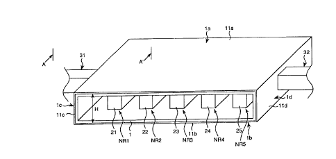
Fig. 1 is a perspective view illustrating the
exterior of a dielectric integrated NRD waveguide
superconducting band-pass filter apparatus according to a
first embodiment of the present invention. A front view
thereof is shown in Fig. 5, and a plan view thereof is
shown in Fig. 6. In Figs. l, 5 and 6, a dielectric
housing 1 made of dielectric materials, such as ceramics
having a high dielectric constant, such as Ba(Sn,Mg,Ta)03
or (Zr,Sn)Ti04, is formed integrally in such a way that
dielectric waveguides 21, 22, 23, 24 and 25, each of which
has a rectangular-prism shape, are interposingly disposed
between an upper surface portion la and a lower surface
portion 1b in the shape of flat plates which face each
other, with predetermined spaces S (the spaces S are not
necessarily equal) each according to a coupling
coefficient. Both end portions positioned at the
longitudinal end portions of the upper surface portion 1a
CA 02198963 1999-09-22
-14-
and the lower surface portion 1b are respectively
connected by two end surface portions 1c and ld, and the
longitudinal cross section is formed in a shape like a o
S symbol with the entire apparatus being rectangular-prism
shaped. Here, the dielectric waveguides 21, 22, 23, 24
and 25 are arrayed in such a way that the longitudinal
direction thereof is parallel to the direction of the
width of the upper surface portion 1a and the lower
surface portion lb, and both longitudinal ends of each of
the dielectric waveguides 21, 22, 23; 24 and 25 are
separated by a predetermined distance from respective
widthwise edges of both the upper surface portion la and
the lower surface portion 1b. The dielectric housing 1
can be formed by firing, for example, a machined or
inj ection-molded Ba ( Sn, Mg, Ta ) 03 .
Flat-plate-shaped superconducting electrodes 11a and
11b, which are superconducting thick films which have a
thickness of, for example, 3 um and which are made of
superconducting materials of, for example, YBCO
(ytterbium carbonate), are formed in close contact by an
evaporation method at the outer surfaces of the upper
surface portion 1a and the lower surface portion 1b,
respectively. Flat-plate-shaped superconducting
electrodes 11c and 11d, which are superconducting thick
films which have the same thickness and materials as
those of the superconducting
02198 963
- 15 -
electrodes 11a and 11b, are formed in close contact at two
end surface portions 1c and 1d, respectively, by an
evaporation method in order to increase the mechanical
strength and shield electromagnetic fields. Here, the
space H between the superconducting electrodes 1a and lb
which are the upper and lower plane electrodes is set at a
half-wave length or less of the center frequency in a
vacuum of the relevant filter apparatus. The
superconducting electrodes 11c and 11d may be electrodes
made from metallic materials of Au, Cu or the like.
As shown in Figs. 8A and 8B, in the central portion
of the end surface portion 1c, a rectangular-shaped hole
31h is formed in such a manner as to open in the direction
of the thickness of the end surface portion lc and the
electrode llc. A rectangular waveguide 31 which is formed
with an upper surface portion 31a and a lower surface
portion 31b which form an E plane, and two side surface
portions which form an H plane are connected to the hole
31h by using a flange 31f thereof. Meanwhile, in the
central portion of the end surface portion ld, a
rectangular-shaped hole (not shown) is formed in such a
manner as to open along the direction of the thickness of
the end surface portion 1d and the electrode 11d, and a
rectangular waveguide 32 formed with upper and lower
surface portions which form an E plane and two side
-16-02198963
surfaces which form an H plane is connected to the hole by
using a flange thereof.
Fig. 7A shows a transmission electromagnetic-field of
a rectangular waveguide having a TEpl mode. In this
embodiment, an LSEpl mode resonator is coupled to the TEp1
mode rectangular resonator, as shown in Figs. 8A and 8B.
This is because the electromagnetic-field vector when the
LSEpl mode resonator is seen from the end surface thereof
coincides satisfactorily with the electromagnetic-field
within the cross section in the TEpl mode. More
specifically, the horizontal components of the electric-
field vector intersect at right angles to the vertical
components of the magnetic-field vector, and the vertical
components of the electric-field vector intersect at right
angles to the horizontal components of the magnetic-field
vector. The direction of the electric-field of the
rectangular waveguide coincides with the direction of the
electric-field of the resonator, whereas the direction of
the magnetic-field of the rectangular waveguide coincides
with the direction of the magnetic-field of the resonator.
In the present band-pass filter apparatus, NRD
waveguide resonators NR1 to NR5 having an LSEpl mode and a
predetermined resonance frequency are formed by the
dielectric waveguides 21, 22, 23, 24 and 25 interposed
between the superconducting electrodes 1a and lb, and the
-1'-02198963
NRD waveguide resonators NR1 to NR5 are formed as band-
pass filters each having a predetermined pass band. Here,
two adjacent resonators are electromagnetically coupled,
and whereas the rectangular waveguide 31 is
electromagnetically coupled to the resonator NR1 at the
initial stage, the resonator NR5 at the final stage is
electromagnetically coupled to the rectangular waveguide
32. As a result, a band-pass filter apparatus comprising
cascaded band-path filters at five stages is disposed
between the rectangular waveguide 31 which is an input
transmission waveguide and the rectangular waveguide 32
which is an output transmission waveguide.
The upper surface portion la and the lower surface
portion 1b of the dielectric housing 1 has only the
function of supporting the superconducting electrodes 11a
and 11b formed on the outer surfaces thereof and does not
have the function of forming an NRD waveguide
superconducting band-pass filter apparatus. Therefore,
the thicknesses t of the upper surface portion 1a and the
lower surface portion lb are formed so as to be
sufficiently thin in comparison with the space H between
the superconducting electrodes 11a and 11b which are the
upper and lower plane electrodes. As a result, it is
possible to prevent a phenomenon in which the resonance
mode of the NRD resonators which constitute each NRD
._ - 18 -
02198 963
waveguide band-pass filter is interfered, and the no-load
Q deteriorates.
Since the main purpose of the two end surface
portions 11c and 11d is to support the superconducting
electrodes llc and 11d (or metallic electrodes) for
shielding an electromagnetic field, their thickness is
formed sufficiently thin within the range in which the TEpl
mode mechanical strength is maintained. In this
embodiment, the rectangular waveguide is formed so as to
be coupled to the side of the LSEpl mode resonator, as
shown in Figs. 8A and 8B.
In this embodiment, since the superconducting
electrodes 11a, 11b, 11c and 11d are used, the ambient
temperature of the present apparatus is cooled to a low
temperature of, for example, 77K by using nitrogen gas or
the like so that the superconducting electrodes lla, 11b,
11c and 11d are operated with a low loss.
Next, a method of setting each parameter in the
filter apparatus of this embodiment will be described with
reference to the accompanying drawings.
Fig. 21 is a graph illustrating the frequency
characteristics of the attenuation constant of
electromagnetic waves when the right-to-left width
direction of the dielectric waveguide intersecting at
right angles to the transmission direction thereof is seen
- -19- 02198963
in the LSE mode, the LSM mode and the TE mode. The
calculation conditions for simulation in Fig. 21 are set
as follows: a space H of 5.0 mm between each pair of
dielectric waveguides 21 to 25, a width W of 2.5 mm, and a
specific inductive capacity ~r of 24.
Fig. 22 is a graph illustrating the frequency
characteristics of the phase constant in the LSE mode, the
LSM mode and the TE mode. The calculation conditions for
simulation in Fig. 22 are set as follows: a space H of 5.0
mm between each pair of dielectric waveguides 21 to 25, a
width W of 2.5 mm, and a specific inductive capacity Er of
24.
Fig. 23 is a graph illustrating the frequency
characteristics of the attenuation constant of
electromagnetic waves when the right-to-left width
direction intersecting at right angles to the transmission
direction of the dielectric waveguide is observed in the
LSE mode, the LSM mode and the TE mode. The calculation
conditions for simulation in Fig. 23 are set as follows: a
space H of 5.0 mm between each pair of dielectric
waveguides 21 to 25, a frequency fp of 12 GHz, and a
specific inductive capacity Er of 24.
Fig. 24 is a graph illustrating the waveguide width
characteristics in the LSE mode, the LSM mode and the TE
mode. The calculation conditions for simulation in Fig.
- -20- ~2198963
24 are set as follows: a space H of 5.0 mm between each
pair of dielectric waveguides 21 to 25, a frequency fp of
12 GHz, and a specific inductive capacity Er of 24.
Fig. 25 is a graph illustrating the characteristics
of the coupling coefficient with respect to the space S of
two arrayed dielectric waveguides. The calculation
conditions for simulation in Fig. 25 are set as follows: a
space H of 5.0 mm between each pair of dielectric
waveguides, a width W of 2.5 mm, and a specific inductive
capacity ~r of 24.
(1) Space H between the superconducting electrodes 11a
and 11b
The space H is set to one half the resonance
wavelength or less in a vacuum of the present filter
apparatus. By setting the space H to such limitation
conditions, it is possible to set the space between the
dielectric waveguides, i.e., the outer portion of each
pair of dielectric waveguides 21 to 25, to be a cut-off
region.
(2) Width W of the dielectric waveguides 21 to 25
The width W of the dielectric waveguides 21 to 25
determines the attenuation constant of waves when seen
from the right-to-left width direction intersecting at
right angles to the transmission direction. For example,
in a case of a waveguide having a space H of 5.0 mm using
_ -21- ~2198963
a dielectric material having a specific dielectric
constant ~r of 24, when the frequency is 12 GHz, the
attenuation constants are as shown in Fig. 23, and by
increasing the width W of the waveguide, it is possible to
sharpen the attenuation in the width direction. Also, as
shown in Fig. 21, the higher the frequency, the greater
the attenuation constant of each mode. Furthermore, as
shown in Fig. 24, the phase constant of each mode reaches
a saturated state when the width W of the dielectric
waveguide increases to a certain degree.
(3) Lengths L of the dielectric waveguides 21 to 25
The lengths L of the dielectric waveguides 21 to 25
are determined on the basis of resonance frequencies to be
set in each of the resonators NR1 to NR5. The resonance
frequencies are determined so that the dielectric
waveguides 21 to 25 resonate at substantially a half-wave
length or an integral multiple of a half-wave length,
including attenuated waves, in the front-to-back direction
when seen from the end surface, with respect to the length
L of the dielectric waveguides 21 to 25.
(4) Space S between each pair of dielectric waveguides 21
to 25
The space S between each pair of dielectric
waveguides 21 to 25 determines the coupling coefficient
between two adjacent resonators. As shown in Fig. 25, the
-22-02198963
narrower the space S of the waveguides and the smaller the
attenuation constant in the cut-off region, the greater
the coupling coefficient. The graph in Fig. 25 shows the
coupling coefficient K, with the waveguide space S as a
variable, in a case where the NRD waveguide resonators NR1
to NR5 are formed using materials of a specific dielectric
constant Er of 24 with a space H of 5.0 mm and a waveguide
width W of 2.5 mm. As is clear from Fig. 25, when the
waveguide space S is set at 5.0 mm, the coupling
coefficient K becomes approximately 0.4~.
(5) Thickness t of each of the sections 11a, 11b, 11c and
11d of the dielectric housing 1, formed using dielectric
materials
The thickness t is set so as to maintain the
mechanical strength required to perform the above-
described functions. When the thickness t is thick to a
certain degree in comparison with the space H, there is a
tendency for the sharpness of the attenuation constant in
the cut-off region to decrease, and the coupling
coefficient K to increase.
The frequency characteristics (i.e., the divergence
relation) of the phase constants of the NRD waveguide
resonators constructed as described above are as shown in
Fig. 22. As is clear from Fig. 22, a TElp mode (basic
mode), a secondary LSEpl mode, and a tertiary LSMpl mode
-23_ 02198963
occur in this order starting from the low frequency side.
The LSEpl mode and the LSMpl mode have cut-off frequencies
f~1 and f~2, respectively; however, in the TElp mode,
propagation is based on a direct current. Therefore, in
the first embodiment, when, for example, a resonator
having an LSEpl mode is formed, a resonator having an LSEpl
mode as a main mode can be formed by setting the center
frequency of the present filter preferably between the
cut-off frequency f~l and the cut-off frequency f~2 and by
adjusting each of the above-described parameters so as to
suppress spurious modes other than the LSEpl mode. Also,
in the second embodiment, when, for example, a resonator
having an LSMpl mode is formed, a resonator having an LSMp1
mode as a main mode can be formed by setting the center
frequency of the present filter apparatus to the cut-off
frequency f~2 or higher and by adjusting each of the above-
described parameters so as to suppress spurious modes
other than the LSMpl mode.
Next, the electric-field distribution, magnetic-field
distribution, and electric-current distribution in the
transmission mode of each transmission waveguide are shown
in Figs. 10A and lOB, Figs. 12A, 12B, and 12C, and Figs.
14A, 14B, and 14C, respectively. A description will be
given below of the electric-field, magnetic-field, and
electric-current distributions in the transmission mode of
02198 963
.- - 24 -
each transmission waveguide.
(A1) Transmission waveguide (Figs. 10A, 10B and 10C) in
the LSEpl mode
In the LSEpl mode, an electric-field vector is present
only within the plane parallel to the propagation
direction and vertical to the superconducting electrodes
lla and 11b which are the upper and lower electrodes.
Electric currents I are generated in the central portion
of the electrodes 11a and 11b which correspond to the
upper and lower surfaces of a dielectric waveguide 26 in
such a manner as to be parallel to the propagation
direction and with the directions being aligned. Further,
at a position deviated by a half-wave length, the front-
to-back directions of the electric currents I interchange.
The superconducting electrodes llc and 11d on the side are
provided for the purpose of shielding electromagnetic
fields, and substantially transmission electric currents I
do not flow through these electrodes 11c and 11d.
(A2) Transmission waveguide (Figs. 12A, 12B and 12C) in
the LSMpl mode
In the LSMpl mode, a magnetic-field vector is present
only within the plane parallel to the propagation
direction and vertical to the superconducting electrodes
lla and llb which are the upper and lower electrodes.
Electric currents I are generated in the central portion
-25-02198963
of the electrodes 11a and 11b on the upper and lower
surfaces of a dielectric waveguide 27 in such a manner as
to be parallel to the propagation direction and with the
directions being aligned. Further, at a position deviated
by a half-wave length, the right-to-left directions of the
electric currents I interchange. The superconducting
electrodes 11c and 11d on the sides are provided for the
purpose of shielding electromagnetic fields, and
substantial transmission electric currents I do not flow
through these electrodes 11c and 11d.
(A3) Transmission waveguide (Figs. 14A, 14B and 14C) in
the TElp mode
In the TElp mode, an electric-field vector is present
only within the plane vertical to the propagation
direction. An electric current I flows radially from the
central portion (of a waveguide 28) of a superconducting
electrode lla on the upper surface, and flows through the
superconducting electrodes 11c and 11d on the side toward
the central portion of the electrode llb on the lower
surface. Further, at a position deviated by a half-wave
length, the directions of the electric currents I of the
superconducting electrodes lla and 11b on the upper and
lower surfaces interchange. Therefore, the electrodes 11c
and 11d on the sides play an essentially necessary role in
causing transmission electric current I to flow.
.- -26- 02198963
Furthermore, Figs. 11A, 11B, and 11C, Figs. 13A, 13B,
and 13C and Figs. 15A, 15B, and 15C show respectively the
electric-field distribution, the magnetic-field
distribution, and the electric-current distribution in the
resonance mode of each half-wave-length resonator in which
dielectric waveguides for each transmission mode are cut
to a finite length and the front-to-back region becomes a
cut-off region. However, the LSEp1 mode used in the first
embodiment and the LSMpl. mode used in the second embodiment
resonate at a half-wave length under an open condition,
and the TElp mode resonates at a half-wave length under a
short-circuit condition. Generally, such a resonator
structure is called a TM11 mode by regarding the height
direction to be the transmission direction.
(B1) LSEpl mode resonator (Figs. 11A, 11B and 11C)
In the LSEpl mode used in the first embodiment,
electromagnetic-field energy concentrates within a
dielectric waveguide 20a, and the outer portion around the
dielectric waveguide 20a is a cut-off region; therefore
energy confinement characteristics are excellent.
Electric currents I are generated centered in the central
portion (of each waveguide) of the superconducting
electrodes lla and llb which are the upper- and lower-
surface electrodes of the dielectric waveguide 20a. The
electric currents I of the superconducting electrodes 11a
- -2~- oz~9e9s3
and 11b on the upper and lower surfaces flow in the same
direction with a plane symmetry and do not intersect each
other. The electrodes 11c and 11d on the sides are
provided for shielding electromagnetic fields, and
substantial transmission electric currents I do not flow
through the electrodes llc and 11d on the sides.
(B2) LSMpl mode resonator (Figs. 13A, 13B and 13C)
The LSMpl mode used in the second embodiment is of a
higher-order mode than LSElp, and the resonator operates in
the same way as the LSEpl mode resonator at frequencies
higher than the cut-off frequency. More specifically,
electromagnetic-field energy concentrates within a
dielectric waveguide 20b, and the outer portion around the
dielectric waveguide 20b is a cut-off region; therefore,
energy confinement characteristics are excellent.
Electric currents I are generated centered in the central
portion of the superconducting electrodes 11a and 11b
which are the upper- and lower-surface electrodes of the
dielectric waveguide 20b. The electric currents I of the
superconducting electrodes 11a and 11b which are the
upper- and lower-surface electrodes flow in the same
direction with a plane symmetry and do not intersect each
other. The electrodes 11c and lld on the side are
provided for shielding electromagnetic fields, and
substantial transmission electric currents I do not flow
-28 02198963
through the electrodes 11c and 11d on the sides.
(B3) TM11 mode resonator (Figs. 15A, 15B and 15C)
In the TM11 mode, a concentrated electric-field vector
is parallel to the height direction of the dielectric
waveguide 28. An electric current I flows radially from
the central portion of the electrode 11a of the upper
surface, and flows through the electrodes 11c and 11d on
the sides toward the central portion of the electrode llb
on the lower surface. Further, at a position out of a
half cycle, the directions of the electric currents I
interchange. Therefore, the electrodes 11a and 11b on the
side play an essentially necessary role for causing
electric current I to flow.
In the first embodiment, a band-pass filter apparatus
is formed by using the above-described LSEpl mode
resonator, whereas in the second embodiment, a band-pass
filter apparatus is formed by using the above-described
LSMpl mode resonator. Concerning the mode notation
convention for the LSE and LSM modes in the present
specification, the first subscript indicates the number of
nodes in the width direction, and the second subscript
indicates the number of nodes in the height direction.
Fig. 2 is a perspective view illustrating the
exterior of a dielectric integrated NRD waveguide
superconducting band-pass filter apparatus according to a
-29-02198963
second embodiment of the present invention. The
difference points of the second embodiment from the first
embodiment are that coaxial connectors 41 and 42 are
provided as input/output terminals, and a coaxial
waveguide 43 is used as a transmission waveguide. The
difference points will be described below.
As shown in Fig. 2, in the central portion of the end
surface portion 1c on the side, a circular-shaped hole 41h
is formed so as to opewalong the thickness direction of
the end surface portion lc and the electrode 11c. A
coaxial connector 41 having a center conductor 41c is
inserted into that hole 41h by using a ring 41f of the
coaxial connector 41. A coaxial plug 43p is attached to
the end portion of the coaxial waveguide 43 comprising a
center conductor 43a and a grounding conductor 43b, and
the coaxial plug 43p is inserted into the coaxial
connector 41, thus the coaxial waveguide 43 is connected
to the coaxial connector 41. Here, the center conductor
43a of the coaxial waveguide 43 is connected to the center
conductor 41c of the coaxial connector 41, and the
grounding conductor 43b of the coaxial waveguide 43 is
connected to the electrode llc via the ring 41f of the
coaxial connector 41. Meanwhile, in the central portion
of the end surface portion 1d on the side, a circular-
shaped hole (not shown) is formed so as to open along the
- -30- 02198963
thickness direction of the end surface portion 1d and the
electrode 11d, a coaxial connector 42 is inserted into
that hole, and a coaxial waveguide (not shown) is
connected to the coaxial connector 42.
The transmission electromagnetic-field distribution
in the coaxial waveguide 43 is as shown in Fig. 7B. The
coaxial waveguide 43 is electromagnetically coupled to the
LSMpl mode resonator NR1 at the initial stage via the
coaxial connector 41 as shown in Figs. 9A and 9B. In a
similar manner, the LSMpl mode resonator NR5 at the final
stage is electromagnetically coupled to the coaxial
waveguide via the coaxial connector. That is, the LSMpl
mode resonator is coupled to the coaxial waveguide having
a TEM transmission mode. This is because the
electromagnetic-field vector when the LSMpl mode resonator
is observed from the end surface thereof coincides
satisfactorily with the electromagnetic-field within the
cross section in the TEM mode. More specifically, the
electric-field vector of the coaxial waveguide 43 has
radius vector components which expand radially, the
magnetic-field vector thereof has components in the
direction of coaxial rotation, and they intersect at right
angles to each other. As described above, since the shape
of the electromagnetic-field vector of the LSMpl mode of
the resonator is similar to that of the cross-sectional
-31- 02198963
electromagnetic-field vector of the transmission mode, an
easy-to-connect structure is formed as an input/output
structure.
Fig. 3 is a perspective view illustrating the
exterior of a dielectric integrated NRD waveguide
superconducting band-pass filter apparatus according to a
first modification of the present invention. In this
first modification, as compared with the first embodiment,
corners 2 in the connecting portions between the upper
surface portion 1a and the end surface portions 1c and ld
and in the connecting portions between the lower surface
portion 1b and the end surface portions lc and 1d are
chamfered so as to form a slope. Meanwhile, the bonding
portions 3 between the dielectric waveguides 21, 22, 23,
24 and 25 on the one side, and the upper surface portion
1a and the lower surface portion lb on the other are
chamfered to be rounded so that a curved line is formed
from the side surfaces of the dielectric waveguides 21,
22, 23, 24 and 25 to the upper surface portion la and the
lower surface portion 1b. As a result, the effect of
preventing cracks when stresses occur in dielectric
materials, and the effect of increasing mechanical
strength can be expected. Factors in which stresses occur
in dielectric materials are present in cases where a
sharp, partial temperature change is given, for example,
02198 963
- - 32 -
in a case in which an increase in temperature when an
electrode is formed as a film has a distribution, causing
a part of the electrode to expand, or in a case where a
decrease in temperature when a superconducting filter is
cooled to about 77K has a distribution, causing a part of
the superconducting filter to contract. Forming a
dielectric integrated type superconducting band-pass
filter apparatus in the above-described way makes stable
operation possible when~this apparatus is cooled from room
temperature (about 300K) to nitrogen temperature (about
77K) so as to operate at a low temperature.
The chamfering in the above-described first
modification may be performed so as to form a slope or
plane surface.
The operation of the filter apparatus of the first
and second embodiments is as follows.
(1) Such filters operate as band-pass filters in the
microwave and millimetric-wave band.
(2) Superconducting electrodes operate with low loss at
low temperatures.
(3) NRD waveguides having predetermined dimensions
resonate at an integral multiple of a half-wave length,
and their ambient regions operate as cut-off regions.
(4) Resonance current concentrates in the electrodes 11a
and 11b on the upper and lower surfaces of the NRD
_ -33 ~2~98963
waveguide, and electric current to the electrode edge
portions is not present.
(5) Such filters operate with the same effects and
advantages with respect to two independent modes of LSE
and LSM.
The details of the effects and advantages of the
first and second embodiments are as follows.
(1) High reliability
Linear expansion coefficients of ceramic materials
are shown in Table 1, and linear expansion coefficients of
metallic materials are shown in Table 2.
Table 1
Linear expansion coefficients of ceramic materials
Ceramic Materials Specific Inductive Linear Expansion
Capacity Er Coefficient ppm/K
(Zr,Sn)Ti04 38 '6 to 7
Ba(Sn,Mg,Ta)03 24 10.7
Table 2
Linear expansion coefficients of metallic materials
(Cited from "Science Chronological Table" (1995) edited by
Japanese National Astronomical Observatory)
-34_02198963
Metallic materials 100K 293K
Copper 10.3 16.5
Brass - 17.5
Stainless steel 11.4 14.7
As is clear from Tables 1 and 2, ceramic materials,
such as (Zr,Sn)Ti04 or Ba(Sn,Mg,Ta)03, have a linear
expansion coefficient substantially smaller than that of
metallic materials. Further, since each section is formed
integrally in the dielectric housing 1 made from ceramic
materials, the linear expansion coefficient of the present
dielectric housing 1 is constant, and this is deformed
analogously when the filter apparatus is cooled.
Therefore, even if the apparatus is operated at low
temperatures, the reliability of the electrical operations
of the filter apparatus is high because internal stress is
small, and problems with cracks in the ceramic materials
or the like do not occur.
(2) Low-loss characteristics
As materials for the dielectric housing 1, dielectric
materials with a low loss at low temperatures, such as
Ba(Sn,Mg,Ta)03 or (Zr,Sn)Ti04, are used. Therefore, when a
superconducting band-pass filter apparatus is formed, the
~219~ 963
- 35 -
low-loss characteristics of superconducting electrodes
effectively act in determining the performance of the
filter. To be specific, when YBCO is used, the surface
resistance value is approximately 10 mS2 at 10 GHz and 50K.
The electrical characteristic values in an example of
dielectric materials are as follows.
(2A) Ba(Sn,Mg,Ta)03:Er = 24, tan8 = 0.114 x 10⁻⁴ (at
a frequency of 10 GHz and a temperature of 77K)
(2B) (Zr,Sn)Ti04:Er~= 38, tan8 = 0.525 x 10⁻⁴ (at a
frequency of 10 GHz and a temperature of 77K)
Further, the temperature characteristics of the
dielectric loss tangent of the above-described two
dielectric materials are shown in Fig. 16. As can be seen
in Fig. 16, the dielectric loss tangent is exceedingly
small at relatively low temperatures.
(3) Ease of process
For example, in a case of a microstrip line resonator
of a comparative example shown in Fig. 18A, six processes
from steps S11 to S16 are required, as shown in Fig. 17B.
On the other hand, for superconducting electrodes of this
embodiment, at least only the upper and lower electrodes
lla and llb of the present apparatus need to be formed;
therefore, as shown in Fig. 17A, it is possible to use
only one step S1 of a simple film-forming process on a
flat surface. Further, since fine-pattern processing is
0219 9fi3
- 36 -
not required, processing accuracy does not pose a problem,
and the reliability of processing accuracy is high.
(4) Electric-power resistivity
Fig. 19 is a graph illustrating the current density
with respect to the position along the width direction in
the microstrip line resonator of the comparative example
shown in Fig. 18A and the NRD waveguide resonator of the
embodiment shown in Fig. 18B. As is clear from Fig. 19,
in the comparative example, abnormal divergence of
electric current appears due to the edge effect in edge
portions 52a and 52b, and a superconducting state is
destroyed in the edge portions when superconducting
electrodes are used; however, in this embodiment, there is
no abnormal current concentration to the electrode edge
portions due to the edge effect. Therefore, even if a
large power is input to the superconducting band-pass
filter apparatus at the critical current density (Jc) or
less of the superconducting electrode, the filter
apparatus is able to operate, and thus it can easily cope
with a large amount of power.
(5) Low-distortion characteristics
As described above, since there is no abnormal
current concentration in the electrode edge portions due
to the edge effect, the linearity of electric power is
improved, for example, the mutual modulation distortion
__ 42998963
- 37 -
becomes small.
(6) Small-size designability
As is clear from Figs. 20A and 20B which illustrate
the relative level of the current amplitude with respect
to the maximum value of the current amplitude, in the NRD
waveguide resonator of this embodiment, energy
concentrates in the dielectric waveguide as compared with
the TM11 mode resonator of the comparative example, and the
attenuation is rapid in-the ambient cut-off region.
Therefore, it is possible to set the coupling coefficient
K between the resonators to be smaller than that of the TM
mode resonator, and the filter apparatus can be made
smaller in size and lighter in weight than the TM mode
resonator.
(7) Thin-type designability
The insertion loss of the band-pass filter apparatus
is almost inversely proportional to the space H between
the upper and lower plane electrodes 11a and 11b; however,
thin-type design is made possible by forming plane
electrodes to be superconductive.
(8) Hybrid formation with plane circuit
As shown in a second modification of Fig. 4, the
surfaces of the superconducting electrodes 11a and llb can
be used in common as grounding electrodes of the other
plane circuits. Therefore, it is possible to form on the
- 02 1 98 9 63
surface of the filter apparatus high-frequency signal
processing circuit modules, for example, oscillation
circuits, frequency conversion circuits, multiplication
circuits or amplification circuits. In the example shown
in Fig. 4, after a dielectric layer 4 is formed on the
superconducting electrode 11a, a pattern electrode 5 and a
terminal electrode 6 are formed on the dielectric layer 4,
thus forming a plane circuit.
Although the above embodiments describe a band-pass
filter apparatus with a five-stage structure, the present
invention is not limited to this example and may be a
band-pass filter apparatus with at least one stage.
Although the above embodiments describe a case in
which superconducting electrodes 11c and 11d are formed on
the sides or on the end surfaces, the present invention is
not limited to this example, and these electrodes may not
be formed.
Each parameter in the embodiment of the
superconducting band-pass filter apparatus employing the
LSEpl mode resonator of the first embodiment is shown
below.
(a) Number of filter stages: 5
(b) Center frequency: 12 GHz
(c) Designed band width: 24 MHz
(d) Ripple: 0.01 dB
-39-02198963
(e) Operating temperature: 77K
(f) Specific inductive capacity of dielectric materials:
24
(g) Space H between superconducting electrodes: 5.0 mm
(h) Width W of dielectric waveguides: 2.5 mm
(i) Space S between dielectric waveguides: 6.0 mm
(j) Length L of dielectric waveguides: 4.2 mm
(k) Filter exterior dimensions = height: 7.0 mm; width:
60.0 mm; depth: 15.0 mm~
The inventors of the present invention realized the
band-pass filter apparatus of the first embodiment by
setting as described above.
In this embodiment, the width W, the space S and the
length L of the dielectric waveguides are fixed values;
however, needless to say, this embodiment may be embodied
by adjusting the respective dimensions for the purpose of
adjusting characteristics.
As has been described above in detail, the dielectric
integrated NRD waveguide superconducting band-pass filter
apparatus in accordance with the first aspect of the present
invention is an NRD waveguide band-pass filter apparatus
having a plurality of NRD waveguide resonators arrayed in
such a way that two adjacent NRD waveguide resonators are
electromagnetically connected to each other, the dielectric
integrated NRD waveguide superconducting band-pass filter
02198 963
- - 40 -
apparatus comprising: a rectangular-cylinder-shaped
dielectric housing including an upper surface portion and a
lower surface portion, and a plurality of dielectric
waveguides, in which a plurality of arrayed rectangular-
cylinder-shaped dielectric waveguides are interposed between
the upper surface portion and the lower surface portion
which are parallel to each other, and the upper and lower
surface portions, and the plurality of dielectric waveguides
are formed integrally; and a first and a second
superconducting electrode formed on each outer surface of
the upper surface portion and the lower surface portion,
wherein the outer portion of each dielectric waveguide is
formed into a cut-off region by setting the space between
the first and second superconducting electrodes to one half
or less the wavelength of the resonance frequency in a
vacuum of the band-pass filter apparatus. Therefore, it is
possible to provide an NRD waveguide band-pass filter
apparatus which is simple in construction and which can be
easily manufactured as well as being formed small in size
and light in weight, and which operates in a single
operating mode. The details of the advantages which are
characteristic of the present invention are as follows.
(1) High reliability
As is clear from Tables 1 and 2, ceramic materials,
such as (Zr,Sn)Ti04 or Ba(Sn,Mg,Ta)03, have a linear
0219 963
°- - 41 -
expansion coefficient substantially smaller than that of
metallic materials. Further, since each section is formed
integrally in the dielectric housing 1 made from ceramic
materials, the linear expansion coefficient of the present
dielectric housing 1 is constant, and this is deformed
analogously when the filter apparatus is cooled.
Therefore, even if the filter apparatus is operated at low
temperatures, the reliability of the electrical operations
of the filter apparatus-is high because internal stress is
small, and problems, such as cracking of the ceramic
materials or the like, do not occur.
(2) Low-loss characteristics
As materials for the dielectric housing 1, dielectric
materials with low loss at low temperatures, such as
Ba(Sn,Mg,Ta)03 or (Zr,Sn)Ti04, are used. Therefore, when a
superconducting band-pass filter apparatus is formed, the
low-loss characteristics of superconducting electrodes
effectively act in determining the performance of the
filter. To be specific, when YBCO is used, the surface
resistance value is approximately 10 mSZ at 10 GHz and 50K.
(3) Ease of process
For example, in a case of a microstrip line resonator
of a comparative example, six processes from steps S11 to
S16 are required, as shown in Fig. 17B. On the other
hand, for superconducting electrodes of this embodiment,
- 42 _ 02 1 98 9 63
at least only the upper and lower electrodes lla and 11b
of the present apparatus need to be formed; therefore, as
shown in Fig. 17A, it is possible to use only one step S1
of a simple film-forming process on a flat surface.
Further, since fine-pattern processing is not required,
processing accuracy does not pose a problem, and the
reliability of processing accuracy is high.
(4) Electric-power resistivity
As is clear from Fig. 19, in the microstrip line
resonator of the comparative example, abnormal divergence
of electric current appears due to the edge effect in the
edge portions 52a and 52b; however, in this embodiment,
there is no abnormal current concentration in the
electrode edge portions due to the edge effect.
Therefore, even if a large power is input to the
superconducting band-pass filter apparatus at the critical
current density (Jc) or less of the superconducting
electrode, the filter apparatus is able to operate, and
thus it can easily cope with a large amount of power.
(5) Low-distortion characteristics
As described above, since there is no abnormal
current concentration in the electrode edge portions due
to the edge effect, linearity of electric power is
improved, for example, mutual modulation distortion
becomes small.
-43- 0219963
(6) Small-size designability
As is clear from Figs. 20A and 20B which illustrate
the relative level of the current amplitude with respect
to the maximum value of the current amplitude, in the NRD
waveguide resonator of the present invention, energy
concentrates in the dielectric waveguide as compared with
the TM11 mode resonator of the comparative example, and
attenuation is rapid in the ambient cut-off region.
Therefore, it is possible to set coupling coefficient K
between the resonators to be smaller than that of the TM
mode resonator, and the filter apparatus can be made
smaller in size and lighter in weight than the TM mode
resonator.
(7) Thin-type designability
The insertion loss of the band-pass filter apparatus
is almost inversely proportional to the space H between
the upper and lower plane electrodes 11a and llb; however,
thin-type design is made possible by forming plane
electrodes to be superconductive.
According to the dielectric integrated NRD waveguide
superconducting band-pass filter apparatus in accordance
with the second aspect of the present invention, in the
dielectric integrated NRD waveguide superconducting band-
pass filter apparatus in accordance with the first aspect
of the present invention, the dielectric housing further
02198 963
- - 44 -
comprises two end surface portions formed in such a manner
as to connect both longitudinal ends of the upper surface
portion and the lower surface portion, and the band-pass
filter apparatus further comprises a third superconducting
or metallic electrode formed on the outer surfaces of the
two end surface portions. Therefore, since the interior
of the present band-pass filter apparatus can be
electromagnetically shielded from the outside, it is
possible to prevent entry of interference and disturbing
waves from the outside, and thus the band-pass filter
apparatus operates stably.
Further, according to the dielectric integrated NRD
waveguide superconducting band-pass filter apparatus in
accordance with the third aspect of the present invention,
in the dielectric integrated NRD waveguide superconducting
band-pass filter apparatus in accordance with the first or
second aspect of the present invention, the upper surface
portion and the lower surface portion of the dielectric
housing, the connecting portion between the two end
surface portions, and the connecting portions between each
dielectric waveguide and the upper and lower surface
portions are chamfered. As a result, the effect of
preventing cracks when stresses occur in dielectric
materials, and the effect of increasing mechanical
strength can be expected. Factors in which stresses occur
0219 963
- - 45 -
in dielectric materials are present in cases where a
sharp, partial temperature change is given, for example,
in a case in which an increase in temperature when an
electrode is formed as a film has a distribution, causing
a part of the electrode to expand, or in a case where a
decrease in temperature when a superconducting filter is
cooled to about 77K has a distribution, causing a part of
the superconducting filter to contract. Forming a
dielectric integrated type superconducting band-pass
filter apparatus in the above-described way makes stable
operation possible when the apparatus is cooled from room
temperature (about 300K) to nitrogen temperature (about
77K) for low temperature operation.
Furthermore, according to the dielectric integrated
NRD waveguide superconducting band-pass filter apparatus
in accordance with the fourth aspect of the present
invention, in the dielectric integrated NRD waveguide
superconducting band-pass filter apparatus in accordance
with the first, second or third aspect of the present
invention, the band-pass filter apparatus further
comprises a plane circuit formed on the outer surface of
the upper surface portion. Therefore, a plane circuit
module for high-frequency signal processing can be formed
on the surface of the filter apparatus, and the entire
apparatus can be formed in a small size and light weight.
0219 9s3
- - 46 -
Many different embodiments of the present invention
may be constructed without departing from the spirit and
scope of the present invention. It should be understood
that the present invention is not limited to the specific
embodiments described in this specification. To the
contrary, the present invention is intended to cover
various modifications and equivalent arrangements included
within the spirit and scope of the invention as hereafter
claimed. The scope of the following claims is to be
accorded the broadest interpretation so as to encompass
all such modifications, equivalent structures and
functions.