Note: Descriptions are shown in the official language in which they were submitted.
WO 96/08086 2 1 9 S 12 3 PCTI[7S95/11045
0
MICROPOWER RF TRANSPONDER
, STATEMENT OF GOVERNMENT RIGHTS
The United States Govemment has rights in this invention pursuant
to Contract No. W-7405-ENG-48 between the United States Department of
Energy and the University of Califomia for the operation of Lawrence
Livermore National Laboratory.
BACKGROUND OF THE INVENTION
The present invention relates in general to radio frequency (RF)
ta~r:sr .~.de ~. !,~,r e partiwiariy, this invention relates to a new
superregenerative micropower RF receiver adaptable for use as a wireless
receiver of a remote contro!-system; and-as- a-mrotely- interrogated-RF
transponder.
Superregenerative type radio receivers are commonly employed in
high frequency, low power reception of radio signals, such as may be
typically used in automotive garage door openen;, portable telephones,
remote meter reading systems, and the like, because of their small size,
ease and economy of construction. Most manufacturers of superregenerative
receivers aim at designing very low power consumption
units, and for mass producing these units at a low cost. Typically, the entire
radio receiver circuit includes one or several inductive elements in addition
to the antenna, and is contained on a single circuit board. The various forms
and types of superregenerative radio receivers that have heretofore been
suggested and employed in the industry have met with varying degrees of
success, particularly because of the limitation cm the inherent power
consumption of these receivers.
A superregenerative receiver or detector is a regenerative circuit in
WO 96/08086 2 19 9 12 5 PCTIUS95/11045
2
which an oscillator is automatically switched between an oscillating state and
a non-oscillating state at a lower rate than the radio frequency. The
switching frequency is referred to as the "quenching frequency". The signal
voltage to be detected is connected to a feedback loop which is connected
to a transistor amprffier to cause oscillation.
In the absence of an applied voltage, the oscillation that builds up
during each cycle of the quench voltage starts with an initial amplitude
detennined by the noise voltages in the input circuit and reaches a final
value con~esponding to the equilibrium value for the oscillation. These
oscilla6ons then fade as the quench voftage prevents oscillating conditions.
More specifically, a conventional superregenerative nroeiver typically
includes an antenna and a superregenerative detector responsive to an
inooming signal received at the antenna It further indudes a buffer amplifier
for amplifying the reoeived signal, a quench oscillator and a low-pass filter.
The quench oscillator also serves as a detector, and the output of the
quench oscillator is derived as a low frequency signal through the low-pass
filter. This low frequency signal is fed to a signal level detector fiuough a
low
frequency amplifier and a bandpass filfer. When the resultant low frequency
=
signal is above a given level, the signal level detector provides an
indication
that the signal has been introduced to the receiver.
A conventional quench oscillator generally includes one transistor and
operates in the following manner. When the transistor is in transition from
its oonductive state to its non-conductive state, the collector voltage of the
transistor increases gradually according to a charging time constant. The
varying collector voltage of the transistor is fed to its emitter via a
capacitor.
If the collector voltage reaches its maximum, i.e., if the current flowing 30
through an oscillating inductor of the quench oscillator is reduced to a
2 199 12 3 pC'T1US95/11045
WO 96/08086
3
minimum, then the base of the transistor is supplied with the bias voltage to
tum the transistor conductive by virtue of the counterelectromotive force
developed by the oscillating inductor. The transistor therefore becomes
conductive abruptly.
Once the transistor becomes conductive, the oscillating inductor
causes a counterelectromotive force to render the transistor non-conductive,
and the collector voltage of the transistor rises gradually. In this manner,
the
transistor is repeatedly switclad betNeen the conduc#ive and non-oorxluctive
states so as to initiate oscillation. In response to such switching, a tuning
circuit produces a transient variation in voltage and current. Under these
circumstances, the output of the buffer ampiifier is applied to the tuning
c rqA to -perFor m asoct of a-mixing operatiost. -A-modutatad stgr-ato rigina-
t ing
from this mixing operation is supplied to the low-pass filter.
Continuous developments are being attempted to improve on existing
supeiregenerative receivers. Examples of such supeKregenerative receivers
and the trend of their development are illustrated in ttie following patents,
all
of which are incorporated herein by reference:
WO 96/08086 ._... 2199623 PCT/US95/11045
4
U.S.Patent No. Patentee Issue Date
U.S. 3,883,809 Ver Planck et al. May 13, 1975
U.S. 4,143,324 Davis _ March 6, 1979
U.S. 4,307,465 Geller December 22, 1981
U.S. 4,393,514 Minakuchi July 12, 1983
U.S. 4,455,682 Masters June 19, 1984
U.S. 4,749,964 Ash June 7, 1988
U.S. 4,786,903 Grindahl et al. November 22, 1988
U.S. 5,029,271 Meierdierck July 2, 1991
The Ver Plandc et al. patent is entitled'!Superregenerative M'ncers and
Amplifiers", and describes a superregenerative circuit including a tunnel
diode. This tunnel diode serves to amplify a radio-frequency input signal and
to mix the input signal with a local oscillation to provide an intermediate-
frequency output The local oscillation is a hamonic of the quench4requency
oscillation applied to the tunnel diode to produce superregeneration.
The Davis patent is entttled'Transistorized Superregenerative Radio
Frequency Detector" and illustrates a transistorized superregenerative radio
frequency detector which utilizes neither biasing circuits nor a base
decoupling capacitor. The detector is self-quenching and operates at a
much higher quenching frequency than was the case for conventional
superregenerative detectors.
The Geller patent is entitled "Digital Communications Receiver", and
describes a reoeiving apparatus for receiving and detecting binary encoded
continuous wave RF signals. The binary signal is detected by a
superregenerative detector. The detected signal and a DC reference voltage are
applied to an amplifier which produces a signal corresponding to the
detected signal but shifted to vary in amplitude about an axis at the DC
WO 96108086 2 199 12 PCT/US95/11045
reference voltage. The shifted signal and the DC reference voltage are
applied to a comparator which produces an output signal at a predetennined
voltage level when the shifted signal is greater than b-e DC reference voltage
and at 0 votts when the shifted signat-is-less than the DC- refemc vo~fage.
5
The Minakuchi et al. patent is entitled "Superregenerative Receiver'
and illustrates a superregenerative receiver whichi includes a quenching
oscillator for converting a received signal into a low frequency signal. The
quenching oscillator comprises a transistor, a positive feedback circuit and
an RC tirne w nstai-it circuit. A circuit is provided for modifying
oscillation
conditions including the base voltage and the RC time constant of the RC
clrou_it
The Masters patent is entitled "Superregenerative Radio Receiver"
and describes a supenegenerative type radio receiver that is particularly
adapted for avoiding fiequency shift of the reoeiver frcm a preselected tuned
frequency. The receiver comprises a superregenerative radio circuit and an
associated anteruna mounted on a circuit board and r eceived in a container
including a wall portion reflective to radio transmissions. The radio receiver
is adapted to be installed near metallic items and maintain tuned frequency
stability.
The Ash patent is entitled "Supemegenerative Detector Having a Saw
Device in the Feedback Circuit", and describes a supcnregenerative detector
ufilizing a single transistor and having a surface acoustic wave device in the
, feed back loop coupling the output to the input to cause oscillation.
' The Grindahl et al. patent is entitled "Remotely Interrogated
Transponder" and illustrates a remotely interrogated transponder which
WO 96108086 PCT/US95111045 =
-- 2 1-9 9 12 3
6
generally includes an oscillator circuit, a deteqtor, a demodulator and a
logic
circxait. The oscillator circuit includes a Colpitts oscillator including a
parallel
tuned tank load capacitively fed back to an amplifying transistor. The tuned
tank is comprised of a shortened half wavelength section of microstrip. An 5
extemal quench circuit comprises an npn bipolar junction switching
transistor. This switching transistor is connected to the source of the
amplifying transistor. The external quench circuit is provided to periodically
tum OFF the amplifying transistor, allowing the oscillations in the tuned bank
to die out.
The Meierdierck patent is entitled "Supen egenerative netector" and
describes an improved supemegenerative detector including input elements
for receiving a high frequency carrier signal having an amplitude envelope
upon which an infonnation signal is impressed. The detector also includes
a first and a seoorui oscillators and output elements for producing an output
signal corresponding to the infamation signal. The detector features the use
of feedback components among the output elements. These feedback
cbmponents include an operational amplifier and reference signal connected
to the first and second oscillators such that the output signal of the
operational amplifier may be used to constrain a transistor that defined the
first amplifier to operate within its linear portion.
These types of superregenerative reoeivers are generally simple and
relatively econornical. However, they suffer from severe disadvantages. In
the first place, even when applied signals are absent, most of these
receivers are continuously tumed ON, and therefore have a relatively high
power consumption, which minimizes their usefulness and limits their
applications. Furthennore, in order for the oscillating circuit to oscillate,
the
losses associated with the resonant frequency determining network should 30 be
lower than the power gain of the oscillator transistor. However, at low
WO 96/08086 219 9123 PCT/US95/11045
7
cxurent levels, the gain available from the oscillator transistor is lower
than
the losses in the resonant -frequency determining network, and the
, - - regenerative operation is not possible.
----
-
Therefore, there is an evident and still unsatisfied need for a new
micropower RF receiver which is adaptable for operation at extremely -low
current levels.
SUMMARY OF THE INVENTION
Accordingly, it is an object of the present invention to provide a new
RF receiver vsh:ch addresses the problems associated with conventional
superregenerative receivers, and which provides adequate solutions thereto.
It is another object of the present invention to provide a new RF
neoeiver which is adaptable for operation at extremely low current levels, and
which has an extremely low power consumption.
It is still another object of the present inverrtion to provide a new
supen+egenerative micropower RF receiver adaptable for use as a wireless
receiver of a remote control system, and as a reniotely interrogated RF
receiver.
It is yet another object of the present inventic-n to provide a new RF
receiver adaptable for use with automotive garage door openers, keyless
entry systems for automotive, home and commercial security systems,
portable and cordless telephones, remote meter reading systems, telemetry
= systems, medical implants such as pacemakers, remote control devices
such as wireless doorbells and fumace thermostats, golf ball tracking,
avalandhe victim location, and like applications requiring the RF receiver to
have an extended useful battery life.
WO 96/08086 2 19 9 12 ~ PCT/US95/11045
8
It is a further object of the present invention to provide a new RF
receiver that is simple and inexpensive.
It is another object of the present invention to provide a new RF 5
transponder which includes minimal inductive elements.
Briefly, the foregoing and other objects are achieved by providing a
new RF reosiver which includes an external quench oscillator for generating
a series of pulses at a predetermined quench frequency, and a pulse forming
network connected to the quench oscillator for converting the series of
perioL,+ic pu!sns into a series of exponentially damped drive pulses. An
oscillator is comected to, and driven by these drive pulses, and an antenna
is connected to the oscillator for receiving modulated RF signals.
A signal extraction network is also connected to the oscillator for
blocking the quench frequency signals, and for passing the detected RF
signals. A micropower amplifier is connected to the signal extracfion network
for amplifying the detected RF signals. In the preferred embodiment, the
oscillator is a Colpitts oscillator which conducts on the negative polarity
only,
and which is fomned of a transistor. An input coupling network is connected
between the antenna and the Colp'~tts oscillator. A logic interface and a data
logic circuit are connected to the micropower amplifier for proeessing the
amplified RF signals. The micropower amplifier includes a self-stabilizing
ampi'fierwhich is compr+sed of one or more CMOS inverters operated in the
iinear mode, and a current regulating circuit connected between the power
supply and the power supply pin Vm, for automaticaliy maintaining the
amplifier at a very low current level. Another embodiment of the RF receiver
includes a self-resonant
inductor or tuned circuit, typically in the range of 0.1 to 1 microHenry with
a
2 19'" 12 3 PCTIUS95/11045
~WO 96/08086
9
resonance frequency on the order of 300 MHz, for defining the operating
frequency of the RF receiver, and for receiving modulated RF signals. A
slightly forward biased Schottky detector diode is connected between the
self-resonant tuned circuit and a micropower amplifier which passes
detected audio or data pulses.
Yet another embodiment of the inventive RF receiver includes a
receive antenna for reoeiving RF signals, typically on ttie order of 300 MHz,
and a frequency selecting netuvork, connected to the receive antenna, for
detenrining one or more desired tuning frequencies. A sampling mixer is
connected to the frequency selecting network for periodically sampling the
modulated RF signals in orcterto obtain a sampled replica of the RF signals.
The frequency selecting network acts as an iimpedance matching
network, for providing a matched termination to the antenna and a high
impedance output to match the average impedance of the sampling circuit.
The frequency selecting network has a relatively long unloaded output
period wherein it acwmulates and stores RF energy during the non-
conductive sampling intetval, and, at the time of sampling, the stored energy
is substantially extracted.
The sampling mixer samples the modulated RF signals at multiples
of the sampling frequency, as indicated by the followirig equation:
F(Sig) = F(RF) - nF(LO),
where F(Sig) is the detected RF signal frequency; F(RF) is the RF filtering
frequency of the frequency selecting network; n is an integer, and F(LO)
CA 02199123 2006-05-23
is the sampling frequency set by a local oscillator, typical(y on the order of
30~ KHz
5 Typically, the sampling mixer is formed of two Schottky diodes in a
common.cathode configuration, such that a local oscillator gate pulse is fed
to the common cathode of these Schottky diodes. A pulse generator is
driven by the local oscillator for increasing the switching speed of the
square wave oscillation signal. A pulse forming network is connected
10 between the pulse generator and the common cathode of the Schottky
diodes for c:onver6ng the oscillation square wave signal at the output of the
pulse generator into a high.peak current signal with a fast rise time and an
exponentially decay'tng tail.
According to an aspect of the invention there is provided an RF
receiver comprising an external quench oscillator for generating a series
of quench oscillation pulses at a predetermined quench frequency, the
RF receiver comprising a) a pulse forming network which acts as a
differentiator connected to said quench oscillator for converting said
series of quench oscillation pulses into a series of exponentially damped
drive pulses, b) an RF Colpitts oscillator comprising a bipolar transistor
connected to, and driven by said drive pulses, c) an antenna, connected
to said RF oscillator, for receiving modulated RF signals, d) a signal
extraction network, connected to said RF oscillator, for blocking said
quench frequency signals and for passing detected RF signals, and e) a
micropower amplifier, connected to said signal extraction network for
amplifying said detected RF signals.
The foregoing rec:eivers can be made part of a transponder for use '
in a variety of applications, such as in automotive garage door openers,
keyless entry systems, portable and cordless telephones, remote meter
reading.systems, telemetry systems, medical implants, and remote control
devices.
CA 02199123 2006-05-23
10a
BRIEF DESCRIP
TION OF THE ORAWiNGS
The above and other features of the present invention and the
maruw of attaining them, wilt bec:ane apparent, and the invention itsetf will
be best understood, by referecloe to the following description and the
acx:ompanying drawings, wlierein:
Figure 1 is a circuit diagram in a block diagram form of an RF
receiver ac:cording to the present invention;
Figure 2 is a more detailed circuit diagram of a first embodiment of
the RF receiver of Figure 1;
WO 96108086 2 1 9 9 " 2 3 PC'T/US95/11045
11
Figures 3A through 3E illustrate various wavE:forms at different stages
of the RF receiver of Figures 1 and 2;
Figures 4A through 4C illustrate various designs for a micropower
= 5 amplifier used in the RF reoeiver of Figures 1 and 2;
Figure 5 is a block diagram of a transponder comprising the RF receiver
of Figures 1, 6 and 7;
Figure 6 is a circuit diagram of a second embodiment of the RF receiver
ac ordina to the present invention; and
Figl.ire 7 is a circuit diagram of a third embodiment of the RF receiver
according to the present invention.
DETAILED DESCRIPTION OF THE PREFERRED EIVIBODtMENTS
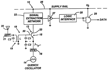
. Figure 1 illustrates a circuit diagram of an RF receiver 10 according to
the present invention. The receiver 10 generally includes a Colpitts
oscillator
12 which is pulsed, or quenched by an external square wave quench oscillator
14 operating at a predetennined frequency, such as 50 KHz. A pulse forming
network (PFN) 16 is connected between the quench oscillator 14 and the
Colpitts oscillator 12 to supply an exponentially damped drive pulse to the
Colpitts oscillator 12, which conducts on the negative polarity only. The
Colpitts
oscillator 12 is fomied of a transistor 15 and the intemal capacitanoe Cl and
C2
(shown in broken lines) of the transistor 15.
The frequency of the quench oscillator 14 is optimized to the Q of an RF
tuned circuit 18. defined by the inductance L of an input coupling network 19
= which could be a part of an antenna 20, and the intemed capacitances Cl and
C2. The frequency of the quench oscillator 14 is also optimized to the
WO 96/08086 - 2-199 12 3 PGT/[TS95111045
12
RF oscillations. A bandpass filter 21 is generally comprised of an LC
network, which may include a parasitic capacitance C3 and the inductance
L, and is connected between the antenna 20 and the input coupling network
19. A helical resonator or a surface acoustic wave (SAW) filter (not shown)
-may optionally be inserted between the antenna 20 and the input coupling
network 19, to further increase the signal selectivity.
Since the Colpitts oscillator 12 is repeatedly stopped and
resynchronized by the quench oscillator 14, whenever a modulated RF
signal is received by the antenna 20, a signal related current is caused to
flow into a signal extracEion network 22 cornected between the coiiedor 23
of the transistor 15 and a power supply rail 25. The signaf extraction network
22 blocks tha RF and quench frequencies, and passes the lower modulation
frequency signals.
A micropower amplifier 27 receives these modulation frequency
signals from the signal extraction network 22, amplffies and passes them to
a logic interface 28, and therefrom to a data logic circuit, such as a
standard
CMOS logic circuit 29 for data prooessing.
Unlike conventional circuits that use a sinusoidal quench waveform,
the receiver 10 uses damped exponential signals generated by the pulse
forming network 16. These damped exponential signals particularly enable
the operation at very low cunent levels. Additionally, with the base 30 of the
transistor 15 at ground potential through the input coupling network 19, the
full voltage of the supply rail 25 appears across the base-collector junction
of the transistor 15 for optimum operation. The receiver 10 uses fewer
components than conventional receivers, and eliminates the traditional bulky
inductors used in quench oscillators.
WO 96108086 2 1 9 9 12 3 pCT1uS95111045
~ .
13
Figure 2 is a more detailed cinxiit diagram of a first embodiment of the
RF receiver 10 illustrated in Figure 1. The circuit ciiagram in Figure 1 is
different from the circuit diagram in Figure 2 in that the input coupling
network 19 is connected to the base 30 of the tr=dnsistor 15 in Figure 1,
while
it is shown connected to the collector 23 in Figure 2. Such difference is
presented for illustrating the various design possibilities of the circuit
diagram, with the preferred embodiment being illustrated in Figure 2. The
input coupling network 19 in the preferred embodiment also serves as the
receive antenna.
In order for the Colpitts csciltatoi 12 to oscillate, the power losses
associated with the resonant frequency determining network comprised of
the input coupling inductance L, the parasitic capacitance C3, and the
intemal capacitors Cl and C2, should be lower than the power gain of the
osciAator transistor 15. For this purpose, the quench oscillator 14 is placed
extemally relative to the Colpitts oscillator 12. The resonant frequency
determining network uses the parasitic capacitance C3 and the internal
capacitances Cl and C2 of the transistor 15 as the feedback path in order
to minimize losses associated with additional extecnal capacitances.
The supemegenerative oscillator/neoeiver does iiot include a separate
quench oscillator inductor. For this purpose, the quench osci!lator 14 is
formed of CMOS inverters using resistors and capacitors to determine the
oscillation frequency. FurthenTiore, in order to achieve a very low operating
power, minimal capacitance elements are used in the carcuit design, by using
the intrinsic parasitic capacitance of the transistor 15 and the distributed
parasitic capacitance C3 of the input coupling network 19.
In the preferred embodiment, the quench oscillator 14 generally
inGudes two inverters 40, 41 (11=74HC04) connected in series; a resistor 42
WO 96/08086 -219 9123 PGT/US95/11045
14
(R=4.7 megohms); a capacitor 43 (C=2 picofarads) connected between the
output of the inverter 40 and the resistor 42; and another capacitor 44 (C=33
picofarads) connected between the output of the inverter 40 and ground.
The pulse forming network 16 includes a first resistor 45 (R=1 kilohms)
5. connected at one end to the emitter of the transistor 15 and at the other
end
to a second resistor 46 (R=47 kilohms) and a capacitor 47 (C=33
piooffarads). The resistor 46 is grounded, and the capacitor 47 is connected
to the output of the inverter 40.
The signal extraction network 22 includes a resistor 48 (R=220
kilohms) connected between the supply rail 25 and the input coupling
network 19. It further includes a coupling capacitor 49 (C = 0.1 microfarad)
connected betwean the input coupling network 19 and the amplifier 27; and
a bypass capacitor 50 (C = 44 picofarads) connected between the resistor
48 and ground. The signal extraction network 22 blocks the RF signals from
the -Colpitts oscillator 12 from being coupled to the amplifier 27, while
passing the lower frequencies which correspond to the data to be output by
the reoeiver 10. The envelope representing the desired data signal appears
at the output of the signal extraction network 22, and is illustrated in
Figure
3E.
Figures 4A, 4B, 4C show three exemplary altemative designs for the
micropower baseband amplifier 27. It should be dear that other designs are
also possible. An important feature of the amplifier 27 is the inclusion of a
cun-ent regulating circuit between the supply rail 25 (VS) and the power
supply pin VDDof an ampiifier 51. The current regulating circuit includes a
resistor 53 having a very high resistance value (such as 10 megohms)
connected between the supply rail 25 (VS) and the power supply pin V., as
well as a bypass, capacitor 52 (C = 2 microfarads) connected between the
power supply pin V. and ground.
~-2199 123
~WO 96108086 PGT/US95J11045
The current regulating circuit automatically maintains the amplifier 51
at a very low current level despite of production variations in the CMOS
circuit, temperature variations and the power supply variations. It should be
5 understood that, in an alternative design, the resistor 53 can be replaced
with a constant current source without departing f'rom the scope of the
present invention.
The amplifier 51 includes one or more conventional CMOS inverters
10 (12 = 74HC04 or MC14069) operating in the linear mode. While Figure 4A
i!l;.sh,ates multiple CMOS inverters (i.e., 54, 55), it ali;ald be uride~
~tood that
any odd number of inverters can altematively be selected.
In order to cause these inverters 54, 55 to operate in the linear mode,
15 an extemal feedback resistive path 56A is provided between the output and
input of the ampl'fier 51, i.e., between points X-X This resistive path can be
designed in a multitude of ways, three of which are ilhistrated in Figures 4A,
.B, and C, and referenced by 56A, 56B and 56C, respectively. These
extemal feedback resistive paths cause the inverters 54, 55 to operate in a
linear mode, and further cause the output voltage of the amplifier 51 to be
equal to Vm/2.
The feedback path 56A is illustrated as the preferred mode in Figures
2 and 4A. It includes a resistor 60, having a rE:sistance of about 22
megohms, which is connected in series with two diodes 61, 62 (D=1 N4148).
These diodes 61, 62 are connected in parallel to provide a highly resistive
path 63. The feedback path 56B includes two resistors 65, 66, each having
a resistance of about 22 megohms connected in series, and a ground path
connected to the resistors 65, 66 and comprised of a resistor 67 (R = 1
megohm) and a capacitor 68 (C = 0.1 microfarad) connected in series. The
WO 96/08086 2 199 123 PCT/US95/11045
16
feedback path 56C includes a resistance having a very high resistance, for
instance R = 44 megohms.
Turning to Figure 2, the logic interface 28 functions as a voltage level 5
translator, and centers the swing of the output amplifier 27 on the threshold
of the logic circuit 29. The logic interface 28 includes a first resistor 75
(R =
22 megohms) connected between the supply rail 25 and the input of the logic
circuit 29; and a second resistor 76 (R =10 megohms) connected between
the amplifier 27 and the input of the logic circuit 29. The logic circuit 29
includes an inverter (11 = 74HC04). A bypass capacitor CB (C = 10
microfarads) is connected bGtvr~~en the supply rail 25 and ground, for high
frequency stability.
Figure 3A shows one period of the square wave oscillation signal of
the quench oscillator 14, which is supplied to the pulse forming network 16.
As illustrated in Figure 3B, the pulse forming network 16 acts as a
differentiator and converts the square wave oscillation signal in Figure 3A
into a high peak current signal with a fast rise time and an exponentially
decaying tail, and supplies it to the Colpdts oscillator 12. During the fast
rise
time, i.e., periods of high peak current (0.1-1mA), the Colpitts oscillator 12
,:..
is made to oscillate, because the high peak current values increase the
bwmcondudanoe of the transistor 15, which supports osciltation. However,
at some point during the decaying tail in Figure 3B, the Colpitts oscillator
12
is quenched. The quench oscillator 14 oscillates at very low current levels,
but at the same time provides high peak current spikes to drive the Colpitts
oscillator 12.
Figure 3C illustrates that the transistor 15 of the Colpitts oscillator 12
is tumed ON, only when the fast rise signal generated by the pulse forming 30
network 16 is negative, and then for a short period of time. The oscillation
WO 96/08086 -219 912 3 PC'T/US95/11045
~ 17
frequency of the Colpitts oscillator 12 is about 300, MHz. In the present
example, the oscillation frequency of the quench oscillator 14 is about 50
KHz, and quenching occurs for about 20 microsecoiids.
The oscillator 12 oscillates for a brief period of time, and the
oscillation will dampen depending on the Q of the RF i'nput coupling network
19. One definition for Q is the number of cycles it takes the oscillation to
dampen to about 37%. In the present example, thie oscillation period is
about 300 nanoseconds (100 cycles x 3 nanoseconds per cycle), which
represents a small fraction of the total duty cycle of 20 microseconds (i.e.,
1.5% of the duty cycle). This provides an important distinctive feature of
losw
power recovery of the input serial data from the RF transmission link as
received by the antenna 20.
Figure 3D shows typical pulsed RF waveforrns representing digital
data, and Figure 3E shows the recovered data at the output of the receiver
10. Figures 3D and E are on a longer time scale than Figures 3A, B and C.
The pulsed RF signal is synchronously rectified at the base-emitter junction
of the transistor 15, where the pulsed oscillations caused by the quench
oscillator 14 drive the junction in and out of cmnduction to provide
synchronous rectification with the reoeived RF pulms. The presence of the
synchronous RF signal causes an increase in current flow through the
transistor 15, which is extracted and applied to the ampiifier 27 as data.
Thus designed, the micropower amplifier 27 draws minimal current,
on the order of I microampere, that is orders of maignitude lower than the
current drawn by conventional receivers. The overall function of the
micropower ampiifier 27 is that of a baseband ampiifier, which can serve as
an audio or data amplifier. The amplification factor of the illustrated
micropower amplifier is about 1000.
WO 96/08086 1 9 9 1 2 3 PGT/US95/11045
18
One important problematic phenomenon facing conventional
receivers, and addressed by the present micropower amplifier 27, is totem
pole current spiking. This phenomenon is characterized by a high power
supply current spike lm drawn when the output of voltage is at Vm/2. This
current spike can range between 40 to 50 milliamperes, and can cause the
power supply, i.e., a battery to be prematurely drained. By decreasing the
voltage V. the current spike is also decreased, and the ampiification factor
remains generally constant. The present micropower amplifier 27 operates
at a very low voltage Vm due to the current regulating circuit 48, and thus
draws a minimal current and consumes minimal power.
The inventive feature of the present invention is exemplified by low
power consumption of the receiver 10. In the foregoing illustration, one
alkaline battery (Vs=1.5 volt) used as a power source, is expected to last
about 30 years, but is practically limited by the battery's own shelf life.
Figure 5 is a block diagram of a transponder 80 comprising the RF
reoeiver 10 of Figure 1. The transponder 80 includes a receiving antenna,
such as the antenna 20 (Figure 1) connected to the RF receiver 10. It
should be noted that the antenna 20 can be a part of the receiver 10. The
data at the output of the reoeiver 10 is conveyed to a data prooessing
network 82, which processes the data and feeds the processed information
back to a transmitter 84, for transmission over a transmitting antenna 86.
The transmitEer 84 can be a conventional transmitter operating at a low duty
cycle for low average power consumption.
In one exemplary application for the transponder 80, the data pulses
generated by the receiver 10 are decoded by the data processing network
82, which provides an acceptance code identifying the validity of the user's
authorization to use the transponder 80. The data processing network 82
WO 96/08086 '--- 219912 3 PCTIUS95/11045
~ . .
=19
may generate a query to the user's unit, and sends, such query over the
transmitting antenna 84. The user's unit then automatically responds to the
query and transmits the response to the transponder 80, which validates the
accuracy of such response by means of a look-up table. In some
applications, the extemaf DATA can include codes to or from various
instruments. The transmitter 84 is normally OFF.
Figure 6 is a circuit diagram of a second einbodiment of an RF
reoeiver 100 according to the present invention. The receiver 100 generally
includes two cirr.uit sections, one on each side of the line 1-1. The circuit
to
the right of line 1-1 is similartn- the circuit in Figurr 1, aiui tl'ierefore
it will not
be described again. The circuit to the left of line 1-1 inctudes a self
resonant
circuit 101, typically in the range of 0.1 to I microHenry with the resonance
frequency on the order of 300 MHz. The resonant ccrcuit 101 defines the
operating frequency of the receiver 100, and also serves as an antenna in
some applications. The input coupling network 19 in Figure 1 can be applied
to improve the selectivity of the receiver 100.
The reoeiver 100 furttter indudes a Schottky diode 102 that is slightly
forward biased (typically 0.3 volt) by a resistor 103 (R = 2.2 megohms). =
Such forward bias places the operating point of the diode 102 on the diode
IV curve in a region where useful recfification occui s at very low signal
levels. Sinoe the IV curve is non-linear in nature, as the incoming RF signal
varies the voltage across the diode 102, the change in the corresponding
diode cument is predominantiy unipotar, namely the upward current swing is
greater than the downward current swing, and the resi.dting average signal
AI is non-zero, i.e., positive. This current change DI causes a slight shift
in
the forward voltage AV, which is coupled by a capacitor 104 (C = 0.47
microfarad) connected between the diode 102 and the input of the ampiffier
27. The voltage AV is the detected RF signal.
WO 96/08086 - 2 12 3 PCT/US95/11045
- 20
A stray capacitor 105 (shownr in broken lines) averages the rectified
RF pulses. The capacitor 104 is a DC blodcing capacitor that blocks the DC
components from passing to the amplifier 27, but passes the data pulses.
The DC components are removed so that the ampiffier 27 is not driven into
saturation.
The receiver 100 can be less sensitive and less selective than the
receiver 10 of Figure 2, but it consumes much less energy. In the foregoing
illustration, one alkaline battery (Vs=1.5 volt) used as a power source, is
expected to last about 300 years, but is practically limited by the battery's
own shelf life.
Figure 7 is a circuit diagram of a third embodiment of an RF receiver
200 according to the present inverrtion. The receiver 200 generally includes
two circuit secfions, one on each side of line 2-2. The circuit to the right
of
line 2-2 is similar to the circuit in Figure 1, and therefore it will not be
described again. The circuit to the left of line 2-2 generally includes a
receive antenna 202 for receiving RF signals typically on the order of 300
MHz.
The received signals are applied to a frequency selecting network
(FSN) 204, which determines the desired tuning frequency or frequencies,
and which feeds the RF signals to a sampling mixer 206. The FSN 204 acts
as a filter and allows only one or a range of RF frequencies to pass through.
The FSN 204 is generally formed of a resonant LC circuit comprising a
capacitor 207 (C = 5 picofarads) connected in parallel to a tapped inductor
209. This LC circuit acts as an impedance matching network, to provide a
matched termination to the antenna impedance (typically 75 ohms), and to
further provide a high impedance output to match the average impedance
of the sampling mixer 206 (typically 10 kilohms).
~ ~ ~ 9 9 12 3
~O 96/08086 PCTNS95/11045
=
21
This impedance matching allows optimum power transfer to occur.
Additionally, the present FSN 204.has a relatively long unloaded output
period, such that it accumulates and stores energy during the non-
conductive sampling interval. At the time of sampling, a very low impedance
is effectively placed across the FSN 204, which causes the stored energy
to be substantially extracted. Thus, the FSN 204 provides a highly efficient
mixer relative to an unmatched mixer.
The sampling mixer 206 periodically samples thie RF signals to obtain
a sampled replica of the RF signal, which carries the audio or data
information to be conveyed over the transponder lirik. This replica is the
detected RF signal. The sampling mixer 206 samples the received RF
signals at mulfiples of the sampling frequency, as indicated by the following
equation:
F(Sig) = F(RF) - nF(LO),
where F(Sig) is the detected RF signal frequency; F(RF) is the RF
filtering frequency of the FSN 204; n is an integer, and F(LO) is the
sampling frequency set by the local oscillator frequency (typically 300 KHz).
The audioldata bandwidth ranges between 0 and 10 Khiz, while the RF frequency
ranges between 0 and 500 MHz.
The sampling mixer 206 comprises two Schottky diodes 211, 212 in
a common cathode configuration. The anode of the diode 212 is connected
to a low-pass filter 214 for smoothing the audio and/or data signals at the
output of the Schottky diodes 211, 212, and for rejecting the RF and local
osciligtor components. The low-pass filter 214 is comprised of an RC circuit
formed of a capacitor 216 (C = 100 picofarads), and a resistor 217 (R =1
megohm) that are connected in parallel between the anode of the Schottky
.. '
WO 96108086 219' 9 1'2 3 PGT/US95/11045
22
diode 212 and ground. The local oscillator gate pulse is fed to the common
cathode of the Schottky diodes 211, 212 in order to periodically drive them
into conduction and thereby sample the RF signal from the FSN 204. The
output of the sampling mixer 206 is then fed to the amplifier 27 via the
coupling capacitor 49 (C = 0.001 microfarad).
The receiver 200 further includes a local oscillator 225 for generating
typically a 300 KHz square wave or other desired oscillation frequencies, by
means of a crystal 227. The crystal 227 is connected in series to a capacitor
228 (C = 33 picofarads), across a shunt resistor 229 (R =10 megohms) and
across the input and output terminals of an inverter 230 (11 = 74AC04). A
capacitor 232 (C = 22 picofarads) is connected between the input of the
inverter 230 and ground. The supply pin of the inverter 230 is connected to
a power supply V'm via a resistor 233 (R = 47 kilohms). The voltage of the
power supply V'm ranges between 1.1 and 1.9 volts, with a typical value of
1.5 volts. A shunt capacitor 235 (C = 0.1 microfarad) is connected between
the supply pin of the inverter 230 and ground.
The oscillation signal is applied to a pulse generator 250, which
provides the square wave oscillation signal with sharper edges, by
decreasing the rise time of that signal. To this end, the pulse generator 250
includes an inverter 251 (12 = 74AC04) whose input is connected to the
output of the inverter 230, via a capacitor 252 (C =1 nanofarad). A shunt
resistor 253 (R =10 megohms) is connected between the input and output
of the inverter 251. The power supply pin of the inverter 251 is connected
to the power supply V'M, and to ground via a bypass capacitor 255 (C = 0.1
farad).
WO 96/08086 -2-199 12 3 pCTlUS95/11045
~
23
The fast rise time square wave is then fed to a pulse forming network
(PFN) 260 comprised of a capacitor 261 (C = 2 pi(mfarads) connected
between the output of the inverter :251 and the common cathode of the
Schottky diodes 211, 212, which, in tum, is connected to a shunt resistor
262 (R =1 kilohm). The function of the pulse forming network 260 is similar
to that of the pulse fonning network 16 (Figure 1). The pulse forming
network 260 acts as a differentiator and converts the fast rise time square
wave signal at the ou#put of the pulse generator 250 into a high peak current
signal with a fast rise time and an exponentially decaying tail, as
illustrated
in Figure 3B, and applies the latter signal to the common cathode of the
Schottky diodes 211, 212. The negative pulses at the output of the pulse
forming network 260 bias the sampling mixer 206 and drive it into
conduction, causing the sampling of the RF signals received over the
antenna 202.
ft should be noted that the FSN 204 does not exclusively determine
the tuned RF frequency. The main advantages of the receiver 200 are its
extremely low power consumption and its ability to define a precise
fnequency by means of a precise receiving frequency aystal oscillator 227.
In the foregoing iQustration, one alkaline battery (Vs==1.5 volt) used as a
power source, is expected to last about 10 years, but is practically limited
by the batter/s own shelf life.
Some exemplary applications of the present invention include but are
not limited to: automotive garage door openers, keyless entry systems for
automotive, home and commercial security systems, portable and cordless
telephones, remote meter reading systems, telemetry systems, medical
implants such as pacemakers, remote control devices such as wireless
WO 96/08086 PCT/US95/11045
2 199 123
24
doorbells and fumace thermostats, golf ball tracking, avalanche victim
location, and like applications requiring the RF receiver to have multi-year
continuous battery operation.
The foregoing description of the invention has been presented for
purposes of illustration and description. It is not intended to be exhaustive
or to iimif the inventiori to the precise forms described, and other modifica-
tions are possible in light of the foregoing teaching.