Note: Descriptions are shown in the official language in which they were submitted.
~7 03!'(~ S~gO~ 7343 K~t~ur~ tent ~ 9~RTB.BIGGER 1~ oo3~oo2~
.. . C:~3
ii 2 11 9 9 4 4 1
PONEI R-SAVIJ~G MISTHOD At71:1 C~1J~CU1~
. . .
'-
'''
BACRGRWND~ OF T~ 'l'ION
'
1~ ~ield ~f the Inver,tion
The pres~nt in~ention relate~ t~ a wirele~
tr~n~~eiver and,. more pecif~c~lly, to power-s~ving me~hod
and circuit for a wireles~ trans~eiver in 2 wirele~
o~municati~n network.
2. Description of th~ Rel~ted Art
In a radio communi~ation sy~tem, power-~aving control
is nece~sary ~or ~ b~~e ~ta~ion ~nd a ter~inal, especially a
~O ~atte~y-powered ter~inal. A~ an example of ~uch a p~wer-
s~ving method, a power ~ontrol ~y~m for u~e in a radio
mo~ile t~mina1 h~ b~en di~close~ in JapAne3e Pat~nt
UneYA~i~ed Publicati~n No . 1~2~0g31. ~ccording to thi~
con~nticnal sys~em, ~ ~adio receiver and a recep~ion
detector are intermit~tently ~upplied ~ith po~er i~ ~
con~tan~ period, re ulting in ~pproximate a half the power
consumptiGn for reception. On the other hand, in the case
. of off-hook, powe~ i~ ~upplied to a~ le~s~ a re p~nse ~gnal
generato~ and a ~ran~mi~ter so as to all~w tran~mission.
~, .. , .. .... .. ... . .... . .. . . .
~7 O~fO~ 19:11 SSos ~a~ 7~ tsur~l P~tent, ~-~ SMART&BIGGER ~G004~0029
~ I
2 2 ~ 9 9 4 4 1
'- PQ5 230
SUMMARY OF ~E~E I~v~ rIO~
~ ..
, . .
Althou~h the conventiona~ power-~ving sche~e io
cap~ble of redu~ing the power con#umption of each mobile
terminal, we found thdt it still ha~ plenty of room ~or
reduction in power con~umption from the view point of ~he
whole netwvrk including bas~ st~tions and mo~ile te~minal~.
An ob~ect of the px~sent invention is to provide
power-~ving method and ~y~tem which achlev~ a ~ub~t~n~ial
redu~tion in total power ~onsumption o~ ~ network.
Ano~her ob~e~t of the pre~ent invention ~ ~ ~o provide
: a transcei~er whi~h ~n reduce ~he power conswmption in the
case of a wait mode wAere it is wai~ing for reception o~
~:. tr~ n~ ion.
A~cording to an asp~ct of the pre~ent invent ion, a
transceiver provided in each of ~t~tion~ ~or~i~g ~
communication 8ySte~ Lncludes an inpu~ detector ~or
detecting an input signal o~ the tran~ceiver and a power
contro~ler ~o~ powe~ing off the transceiver ~xcept the input
detector in a first ~tate where the input ~ignal i~ not
2Q detected and for powering 4n the trans~elver in a second
'. -'!
~tate wher~ the input siqnal i~ ~etecte~. In c~e~ where
e~h tation i8 in the fir~ te, the tran5ceiver ex~ept
the input detect~r i~ power~d off. There~ore, the tot~l
power con~umptinn of the station~ i~ reduced in the ~irst
~7[)3~ 11 2S~3 3~g~ 7~4~ K~t~ur~i P~tent ~ J SMART&~I~GE~ ~0005~002~
_ '.1
..
~ 3 2~99441
' ' ~
F05--23 D
state. The ~nput detecto~ ~ay be powered on ~nd off in a~ ''
predetermined period in the fir~~ 8ta~e.
According to anoth~r aspect of the p~e~ent invention,
:in a communication ne~work ~omp~i~ing a plurali~y of
.:15 st~ion~ a first station ~e~ects presence or ~en~e of
tran~mis~ion d~ta according to power 6upplie~ to a first
power supply line. In a first ~tate where the t~nsmission
~ata r S no~ detected, ~he fir6~ sta~ion power~ ~ff a secor.d
power supply line. ~n a ~econd state where the tr~n~ sion
da~a i~ detected, ~he firzt st~ion powerS on the ~ir~t and
second power supply lines, and ~hen tranSmits a fra~e sign~l.
comprisin~ the tr~n~mi ~ion dat.a and communication ~e~we~t
data to a second ~t~ion. On the other ha~d, the se~on~
~tation detects presence or absen¢e of the communication
request ~ata from ~e~eption dat~ ac~or~ing t~ powe~ supplied
to a third p~wer ~upply line. In a third s~te where ~he
communication reque~t data is not detected, the second
j~tation power~ ~f~ a ~ourth power supply line. In a fou~t~.
:state where the communi~tion request d~ta iB detected, the
2~ ~e~ond ~t.~ion power~ on the third and fou~th po~er 5upply
~-'lin~s. I~ ~he third ~t~t~, the third power supply line ~ay
be powered on and of~ in a p~edet~ i ne~ period.
~ 03f Ori 18 :11 2S03 3g~ 734~ K~t~ur~l Pulen~ S!L4RTBcBIG;GER ~ 0rJ~, oo~a
. . .'
rr2 79944 1
., '
. ; FC!5- 230
: .
BE~IEi~ DESCRIP~ION O~ THE DR~WIN~S
, ...
Fig. 1 i~ a block diagr~m showing ~n emkodiment of a
transceiver ~ccord~ nq ~o ~he preaent invention,
~,,,
,:
Fig. 2A i~ a diagram showins an e~xample c~f a sontrol
5 signal fra~e ~ormat used in ~he e~odiment;
~ ig. 2s i9 a diagra~ showing an example o~ a da,ta.
signal ~rame forma~; u~ed in ~he em~oclienent;
.
~ig. 3 is ~ schemati~ dia~ram showing an em~odiment
~f a network accc~rding ~o the present invention; and
t O Fig. 4 is ~ t im~ ng cha~t ~howing an operation of the
tran~ ceiver .
DES~RIPTION OF T~IE ~ llBODIM~5NT!;
. .
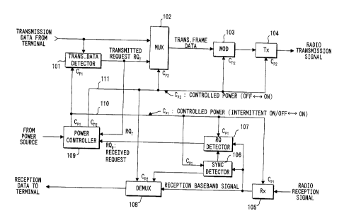
T~ANS(~EIVE~
' Referring to Fig. l, ~ tran~ceiver accor~ing to the
~- 15 ~resent in~ention i~ ~omprised Or a tran~mi~sion c~rcuit, a
recepti~n c:i rcui~ an~ a power cont~oll~. The tr~n~ 810n
c!ircuit i~cludes a tr~n~n ig~ion ~a~a detec~or 101 which
, _ _ , . . . . .
a7 o~lo~ l ~o~ S~86 734~ ~Ht~ur~l Patent ~ SMART8cBIÇ;GER E!10007~0028
; ~
~. 5 2~9944~
Q~-23~
dete~t~ the presence or ~bsence of trAn9mission data
... ..
received from a te~ 1 nAI or a proces~o~ ~not shown) . Wnen
the transmission cl~ta i~ ~eceived, the tran~mi~ i on data
- ~letector 101 ou~puts cammuni~ation reque~t d~ta RQl~ ~o a
;: 5 multip~exer 1~ . Th~ mu~ tiplexer 10~ multiplexe~ the
trAn~mi ~ion datd, the co~unication reguest dc.~a RQ~ and
oth~r nece~sary information to produce a frame of
transmisxLon d~t~ whlch is ~utp~t to a modul~tor 103. The
modul~or 103 modulates a ~ ocal oscillation signal accordin~
to the tr~nam; ~çian fr~me data received from the m~l~iplexe~
-~ 102. A trAn-C~ ion sign~l produçed l~y thF~ modula~or 103 i~
converted to a t~n~ siorl radio fre~ency and tnen
amplified in power by a tr~n~it~er 104. The radio
~ransmis~ion 8i~n~ transmitte~ ~hrough an ant~nn~ ~not
shown~
The rece~ption cirçuit include~ a receiver 105 whic~
receive~ ~ radio reception signal ~n~ demo~lulate~ ~
rec:eption base~and ~iSrnal there~ror~ Th~ rec:eption ~asebe~nd
~igna~ i~ ~upplied ~o a syrl~ ~etectcr 106 and a
communi~ation request (R~) ~ete~or 107~ ~he syn~ detecto~
10~ delect~ ~it ~nd ~rame ~y~chroni~ation from ~he reception
~a~eb~nd signal. AGc~rdi.n~ to the bit and ~Xa~e
- ~ynchronization~ th~ RQ detector 107 de~ects co~mun~ca~ion
- req~e~t d~t~ frcm the reception baseband ~ignal. The
received c~m~unication reque~t d~ta R~ i~ the ~ame a~ ~
-
~~7 0~ 0~ 11 fSo3 3~6 ~g~ K~t~ur~l Patent ~ SILAE~T~BIGGER 1~0008~00~a
: .
,, ~ 2~g~441
~ ~ FQ5-230
tr~n~mi~sion commu;lication ~gue~t data ~Q~ which Wd~i
transmitted ~y the oppo~ite tr~ eive~ communi~ating with
. .
tne ~elevan~ transcei~er~ In this ercbod3menl~, the
-. tran~mitted ~nd receiv~d communication re~ue t data ~Q~ ~nd
- 5 RQ" a~e th~ same data ~2, rOr in~tance, a pr~determined bit
pa~tern or flag. Fur~h~r~ ~ccording to the bi~ an~ frame
synchroni~ation, a dem~lti~lexer 108 dem~lltiplexes re~ep~ion
data from the recep~l on ~a~eband signal and outputs ~he
recep~ion data ~o the t~ ~ l or ~he proce~sor.
The power controller lOg i~ connec~ed t~ ~ pc)wer
supply ~ n~t shown in thi~ ~iguIe) ~ The power ~ontroller 139
- has a ~irst power 8Upp;y line llO and a ~econd poweI~ ~upply
line ill through which cont~olled powert3; C~l and Cp~ are
: ~ . 6upplied, respectively. The respective power~ C7j,~ and CP2 a~e
~ontr~lled accc~rding to ~he transmitted and ~e~ei~red
~O~munication request dat~ RQ~ and RQ~ as will be described
l~ter. The fir~t power supp~y line llO i~ ~onne~ed to the
transmis~ion data dete~tor 10~, the receiver 105, the sync
dete~tor 106 and the ~Q detector 107. ~ha seccn~ power
~0 ~upply line 111 i9 conQected th ~he multiple~er 102, ~he
~dulator 103, th~ tra~,t~er 104, the demultiplexer 10
and otner ~ir¢uits of ~he transceiver.
.' More spe~ificallv, when nei~her the ~ommunica~ion
re~uest d~ta RQ~ nor ~he communication r~quest ~ata RQ~ is
'~ 25 r~ceived, tha~ i~, .in ~ w~it ~ e, the power controlle~ los
... . , . . . , . .. , . . . _ .. .. . .. .. _ . ...
~7 fJS~0~ ~0~ 39~B ~.3~3 K~sur~l Pat~nt ~ ~ ) SM.4RT&BIGGER l~loooa~oo29
~ 7 2~99441
, .
FQ5-230
i nte~ittently ~upE~lies power to the fir~ power supply lin~
110 in a predetermine~l period ~nd do~s not ~upply power to
the se~on~ 3~o~er ~upply line ll~. ThereLvre, the controlled
,
power Cp, of the firat power ~;pply line llO i8 #upplied to
5 the tran~mi~~ion da~a de~ector lOl, the receiver 105, th~s
~~nc detector 106 and the RQ ~e~ec~or 107, ~nd, ~t ~he ~ame
t~me, the other circuits are pc~we~ed of~. In other word~;,
when in the wait 3tate, the ~ransceiver i~ looking at only
the occurren~ o~ tr;~ mi QsiOn or re~eptib~ in a
l 3 pre~ete~min~d period .
When the ~omr~uni~ation re~u~t da'ra ~Q~ OI' ~he
com~unication request d~ta R~A i~; ~e¢eived, the power
controller ~09 power# on the fir~t and ~econ~ powe~ ~upp~y
lin~?~ llO and lll to allow ~oth tran#mission and reception
15 of the tran~eiver. When neither the commllnlca~ion leque~t.
clata RQ~ nor the ~ommunication ~que~t data RQR i~ received
for a pr~detennined ~ pericd, the power controller 109
return~ ~a~k to ~he wait ~tate~
Referring to Fig~, 2A and ZB, the multiplexer 102
multiplexe~ the t~n~; scion data and th~ ~ommuni~ation
reque~t d~ta ~ to produc~ a frame of t~hn~ ion d~ u~h
that the communicat~on request data RQ i~ located in a
synchronization period of the frame with fcllowing
synchronization w~rd ~SYN~ W~ and a preamble (PR).
Therefore, the R~ detector ~07 iB c~pa~le of detectin~ the
... ... . . . .. ...... ~
~7 03 0~ ~8~ 3g8~ T~4~ K~tsur~l P~tent ~ MART&BIGGER Ç~110010~002~
'. = 2~g~4~
O
~ Ey5-230
..
~ommunica~i4n r~que~t da~a RQ from the ~cep~ivn baseband
signal according to the bit ~nd frame synchronization
~upplied ~rom the ~ync detector 106.
~ ~i
NETWORK
A~ shown in Fig. 3, a r~dio communication net~ork is
- ~omp~i~ed of a plurality of base station6 and ~ plurality o~
: termin~l~. Acco~ding ~o the pr~sent in~ention, ~ach
i termindl and each ba~e station are provided with the
tran cei~er as s~own in Fig. 1.
Referring ~o Fig. 3, a ~erminal Tl includes ~
- transceiver 201, a d~ta pr~cesso~ 202 and other nece~~ary
device including a keypad, a speaker and a microphone. A
~ase station BSl i6 p~ovided with a transceive~ 203, A da~a
proces~o~ 204 ~nd othhr nece~sary devices. In thi~
embodLment, the ~a~e ~ation i~ conne~ted to pu~lic swi~ched
telephone network ~PST~) 205. The base ~tation may be
. ~onnected to a ~ub~criber line of a ~witching sy~tem. it i~
.: the sa~e with another ba~e ~tation ~S2. Another terminal T2
inclu~e~ a tran~eiv~ 205 which i6 connected to a ~erminal
PC (pe~onal compu~er~ ~07. Xereinafte~, it is ~umed th~t
the term;n~l ~2 receive~ a calling signal ~rom the termlnal
--
~. Tl th~ough the ba~e ~tation~ BSl and BS2 and the PS~N 205.
. . .
ORI~INATING TE~MINAL
In the tran~ceiver 201 o~ ~he originating ter~in~l Tl,
~ 25 the tran~mis~ion d~ta detector 101, ~ne ~eceive~ lOS, tne
. .
.
, , , ~, . . . . . . . . .
~7 03~0~ 11 ~u3 ~8~ 734~ t6ur~1 Pate~t ~ ,~ SMART&~I~;GER l
-.-,... _.
g ---2 ~9~4
..
FQ5-~ 3 0
_
first power supply line 110 i~ int~rmi~ently powered on and
. ~ i off in ~he predç~termined period and the ~econd power supply
line 111 is not ~upplied with pffwer in ~he wait ~tate.
herefor~, the multiplexer 102, the modul~tor ~03, the
- . .!
.1 5 tran~mitter 104, and the demllltiplexer 1~ are powered o~f
- in the wait ~tate. When the tran~miR~ion dat~ detector lOl
~ detect~ t~n~ sion data including ~he source ad~re~ o~
i~ own and the de~t~nation addre~s ~her~, tne terminal Tl ~,
the multiE~lexer 10~ ~ultiplex~s the ~ran~mission data ~n~
the c:ommunication requeS~ data RQ to pro~uce a ~ra~e o~
tr~:~smi~i~ion dat~ as shown in Fig. 2A. At the same time,
the power corltrol~er 109 ~ully dctiva~e3 all th~ ~ircuit~ of
the tran~ceiver 201 ~o as to allow tr~n~ sion a~d
, reception.
BASE STATIONS
In the ~a~e ~tation ~Sl ~ when ~he tran~ceiver ~03 is
in the ~ait ~t~te, the circuits other than the tran~ ion
data ~etec~or 101, the receiver 1 05, t~e sync de~ector lO~
and the RC~ dete~tor 107 are also powered off. When the
~o ~eceiver 105 receives the ~alling ~ignal ~ro~ the te~i~l
T1 and the RQ detector lQ7 detects thc communication request
data R~ fro~ the ~ey~ion b~seban~ signal, th~ power
.-. cont~ol~er 10~ fully activa~e~ all the circuit~ ~f the
transc:eiver ~0~ so as to ~llow t~ansmi~ion ~nd re~eption.
~uh~equently, ~he proces~4r 204 pro~uce~ tran~mi~sion
-
... . .. , .. . ~ . .. ... .. . . .
~7 03, 0~ 03 3~ 7~43 K~t~;ura~i Patent 1~ SMART&BI~GE~ IZI l)012~002~
,i,,
'~ lo ~2 ~ g944 ~
'::'
~Q5-~ 3 0
,
. ~ data from ~he re~eption data and tr~nC~it~ it to the 1~6e
~- ~tation B~2 through the PSTN ~05. ~n c~ses where thQ
- de6tination addre~s i~ regi~terec~ in it6 memory, the
~.,
~ 1 processo~ 2G4 may pro~uce tr~nc~; ssion data a~re6~ed to the
,~' S ~errin~l ~2 and the trans~eiver 203 ~r~nsmî~s a callin~
- signal includin~ the ~onmunication re~ue~t data RQ to the
tenninal ~2.
Since the base ~tation BS2 ha3 t~2e same configu~tion
a~ the ba~e ~t~tion BSl, the same numeric:al re~erenc~e~ a~
~0 the base statio;l E151 will l~e u~ed. When the ba~e #tatio~
BS2 receive~ a ~ g signal addre8~ed to the terminal 'r2
fro~ the ~ase ~tation BSl throu~h the PSTN 205, ~he
proce~sor 204 produ~e~ t~nRmi ~ion data ~dd~es~ed to the
te-~;n~l T2 and output~ it to the t~dn~ceiver 203. Wllen
receivin~ the tran~i#sion dat~ from the proce~or 204, the
- tran~mis~ion da~ detector 101 produce~ ~he cotmnunic~ation
reques~ data RQ whlc:h is ou~pu~ to the multipl~xer 102 and
the power controller 1os . Tne power con~ro~ ler~ 10~ ~ully
activate~ all the ci~cuite of the transceiver 50 a~ to allow
~ ~0 t:~an~DIis~ioll ~n~ reception.
;,-.
D~;~;TlNATION ~E~MINAL
~ ~hen the transceiv~r 20~ i8 in the wait state, the
.li circuits other than the ~r~n~ sion data detecto~ 101, the
.~.
receiver 105 r the sync detec-~o~ 106 ~nd ~he RQ detecto~ 107
25 are also pow~red o;Ef. In t~e c:ase where the receiver 105
. .
~, .. , . . .. , ... _ . . . ...... ..... . .... . .....
~7 0~/~6 1~ .3~86 T34~ tsur~l P~tent ~ 1 . S~RTB~BIGGEX 1~l~0l3, 002a
,~
1 1 2 ~ 9 ~ 4 4 1
' F~5-230
re~ei~es the ç~l l.i.ng ~ig~al ~r~m the base ~tation BS2 and
the RQ detecto~ 107 detec~ the co~ ation reques~ dat~
:
RQ fl~om ~he rec~ption ~2~eb2lnd signal ~ the power controller
110 fully acti~ate~ all the circuit~ o~ the transceiver 201
5 ~o as to allow tran~mi~fiion ~nd reception.
In thi~ ~anne~, the terminal~ T1 and T~ are allowed
to communic~te with e~ch other. Since a ~ign~l ~rame
include~ the communi~cqti~n reque~t data k~ own în Fig#.
2A ~nd ~B, the re~p~ctiv~? ~ran~ceivers of the terminals Tl
lB and T2 aIld ~he l:~ase sta~i.on~ ~3Sl ~nd ~S~ are fully act~vated
during communieation. When the cammunic!~ion i~ te~mLnated,
the communic~ n request data ~ no longer re&ei~ed.
~rhere~ore, after ~aiting until a 1apse of a predetermined
tL~e period lon~e~ tha~ ~he frame p~riod~ the tr~Bceiver~
r~turn to ~he wait ~tate.
Referring ~ Fig. 4 where an operation of the
t~an~ceiver of F~g. 1 is ~hown~ when no communi~ation
requ~t da~a R~ 1~ re~eived in the wait state, ~he power
~Gntroller 10~ intermit~ently supplieB powe~ to the firs~
- 20 power ~pply }i~e 110 in ~he pr~determin~ p~ri~d and does
, not 6upply power to the second po~er ~upply li~e 111. The
- predetermine~ period may ~e s~t to be approximately the
frame perlo~ T ~ . 125~sec)~ Thi~ c~use. the power
consu~ion o~ ~he first power ~upp~y li~e 11~ to be reduced
~5 ln the wait ~tate~
.. ,, .. : . . .. ~ .. _ . . .. . .. . . .
97 ¢3rlJ~5 18~ T~ K~t~ur~l P~tent ~ SNART~;BI-I~ER 1~lool~oo~
_,
2 ~ 9 9 ~ ~ ~
. . .
FQ5-Z 3 0
When the communication reque~t data R~ is received,
- ! the power controller 109 powers on the fir~t ~nd se~ond
power ~upply line~ liO and 111 to allow tr~n~mi~~io~ and
- ~ re~eption. ~ince the conununicatlon reque~t d~ta RQ is
-; 5 re~:eived during the cc~nanunication~ the first and ~econd
!
powe~ ~upply lines 110 ~nd 111 continue to be po~e~ed on.
Nhen the communic~tion i~ completed, the communi::ation
reque~t data R5; i8 no longer receilred. I~herefore, after
wai~in~ until a lapse of the prede~t~ e-l t~ne period ~r"
longer than the frame period T, the power controlle~ ~O9
return~ to the wait s~ate.
. .
.
., . . ~ , , . _ .