Note: Descriptions are shown in the official language in which they were submitted.
W096/08077 PCT~S95/10886
0 2 1 9 9 5 2 5
DESCRIPTION
Transmission and Reception of CPM Spread-Spectrum Communications
Related A~Dlication Data
This application is a continuation-in-part of
copending U.S. Application Serial No. 08/304,091 entitled
"Coherent and Non-Coherent CPM Correlation Method and
Apparatus," filed on September 9, 1994.
Field of the Invention
The field of this invention relates to spread spectrum
communication and, more particularly, to transmitting and
receiving continuous phase modulated (CPM) signals such as
spread spectrum signals. - -
Description of Related Art
Spread spectrum is a type of signal modulation thatspreads a signal to be transmitted over a bandwidth that
substan~ially exceeds the data-transfer rate, hence the
term "spread spectrum". In direct sequence spread spec-
trum, a data signal is modulated with a pseudo-random chip
sequence; the encoded spread spectrum signal is transmit-
ted to the receiver which despreads the signal. Several
techniques are available for the transmitter to modulate
the data signal, including biphase shift keying (BPSK) and
continuous phase modulated (CPM) techniques. Minimum
shift keying (MSK) is a known variation of CPM.
In despreading a spread spectrum signal, the receiver
produces a correlation pulse in response to the received
spread spectrum signal when the received spread spectrum
signal matches the chip sequence to a predetermined
degree. Various techniques are available for correlating
the received signal with the chip sequence, including
those using surface acoustic wave (SAW) correlators,
W096/08077 PCT~S9S/10~6
2 1 9 9 5 2 5
tapped delay line (TDL) correlators, serial correlators,
and others.
In spread spectrum communication CPM techniques are
often chosen so as to preserve signal bandwidth of the
5 spread spectrum signal when it is amplified and transmit-
ted. Using CPM techniques also has the advantage that
~class C" amplifiers may be used for transmitting the
spread spectrum signal. However, spread spectrum signals
transmitted using CPM are difficult to decode with many
10 types of spread spectrum correlators, including various
SAW correlators and serial correlators. These types of
correlators usually require a BPSK spread spectrum signal
for effective correlation rather than an MSK or other CPM
spread spectrum signal because a BPSK signal has either a
15 zero or 180 degree phase shift for each chip time. Thus,
each chip of a received BPSK signal may be compared with
each chip of the spread spectrum code, and a maximum
correlation pulse may be generated when a predetermined
number of matches occur. However, when a CPM signal with
20 the same data signal and chip rate is applied to the same
correlator, the correlation pulse will generally be very
weak and may be quite difficult to detect.
Another problem often encountered in attempting to
correlate spread spectrum signals transmitted using CPM
25 techniques is the absence of a coherent reference signal
in the receiver. A coherent reference signal in this
sense may be defined as a locally generated signal that
matches the transmitter carrier signal in frequency and
phase. The receiver may use the locally generated refer-
30 ence signal to demodulate the received signal. In prac- r
tice, however, it can be difficult to independently
generate a local reference signal in the receiver precise-
ly matching the transmitted carrier signal in frequency
and phase. Rather, a local reference signal generated in
35 the receiver will usually be of a non-coherent variety --
that is, having small differences in frequency and phase
from the transmitter's carrier signal. These frequency
-
W096/08077 PCT~S95/10886
0 2 1 9 9 5 2 5
and phase differences are not constant but vary over time.
When an attempt is made to demodulate a received signal
using a non-coherent reference signal, errors in correla-
tion may occur due to mismatches in timing and variations
in perceived amplitude caused by the frequency and phase
differences.
Various methods for dealing with the above problem
exist in which a coherent reference signal is created in
the receiver by continuously measuring the frequency and
phase differences between the received signal and a
locally generated non-coherent reference signal, and then
adjusting the non-coherent refere~c~ ~ignal until it
matches the fre~uency and phase of the received signal.
Such methods, however, generally require the use of
relatively complex feedback techniques and involve extra
hardware. Moreover, locking onto the received frequency
and phase can take an unacceptably large amount of time,
particularly in systems where time is of the essence, such
as in certain time division multiple access (TDMA) systems
in which only a relatively brief time slot is allocated
for periodic communication between a transmitter and
receiver.
A particular non-coherent digital matched filter is
described in A. Baier and P.W. Baier, "Digital Matched
Filtering of Arbitrary Spread-Spectrum Waveforms Using
Correlators with Binary Quantization," 2 Proceedinqs, 1983
IEEE Military Communications Conference, Vol. 2, pp. 418-
423 (1983). The digital filter described therein uses
four real filter channels to perform four-phase
quantization in the complex plane, with the four quadrants
being the quantization regions, and the result taking on
the four complex values of +l+j. In the described four-
phase filter, an input signal is divided into an in-phase
signal and a quadrature signal. The in-phase signal and
the quadrature signal are separately filtered, sampled and
digitized using 1-bit quantization. The quantized in-
phase signal and the quantized quadrature signal are each
Wos6/08077 PCT~S95/10886
0 2 1 99 5 2 5
fed into two binary correlators each programmed with a
reference sequence of`N chips, one chip for each sample.
The outputs of the four binary correlators are combined to
produce a resultant output signal. Baier's four-phase
digital matched filter is also described in A. Baier, "A
Low-Cost Digital Matched Filter for Arbitrary Constant-
Envelope Spread Spectrum Waveforms," IEEE Transactions on
Communications, Vol. Com-32, No. 4, April 1984, pp.
354-361.
These references suggest that for demodulation of non-
coherent CPM signals such as QPSK, MSK, OQPSK, and GMSK
signals, four real channels are needed to fully recQYer
the transmitted signal. Further, the described four-phase
filter shows only a system using 1-bit quantization, and
does not describe a technique for serial correlation.
Accordingly, it would be advantageous to provide a
method of modulation and demodulation particularly suited
to CPM signals. It would further be advantageous to
provide a method of CPM modulation and demodulation that
does not require the generation of a coherent reference
signal, that is capable of rapid correlation, and that may
be used with analog correlators and digital correlators in
an effective manner. It would further be advantageous to
provide a flexible and effective system for CPM modulation
and demodulation that does not require a coherent refer-
ence signal, and that is suitable for use in an environ-
ment of cellular communications.
Summarv of the Invention
The invention relates to a method and apparatus for
transmitting and receiving CPM spread spectrum signals
using phase encoding to increase throughput. In one
aspect of the invention, a transmitter divides a signal
data stream into a plurality of data streams (e.g., an I
and Q data stream), independently modulates the data
streams using CPM or a related modulation technique, and
superposes the plurality of resultants for transmission.
W096l08077 PCT~S95/10886
~ 2 1 g 9 5 2 5
A preferred receiver receives the superposed spread
spectrum signal, simultaneously attempts to correlate for
a plurality of chip sequences (such as I and Q chip
sequences), and interleaves the correlated data streams
into a unified signal data stream.
In a second aspect of the invention, the receiver
comprises a carrier signal that is neither frequency
matched or phase matched with the transmitted signal. In
this aspect, the receiver separates the received spread
spectrum signal into real and imaginary parts, attempts to
correlate both real and imaginary parts for a plurality of
chip sequences (e.g., I and Q chip sequences!, and com-
bines the real and imaginary signals into a unified signal
data stream. A preferred embodiment of this aspect of the
invention uses a single bit digitization of the received
spread spectrum signal to preserve only phase information
for inexpensive digital processing. Another preferred
embodiment of this aspect of the invention uses two-bit
digitization of the received spread spectrum signal. In
an alternative embodiment of the invention, the receiver
uses self-synchronization techniques for despreading and
correlation.
These aspects of the invention are described with
reference to a preferred embodiment of the invention, in
which a single parallel correlator and a plurality of 32
serial correlators are combined so as to allow correlation
and recognition of any of 32 distinct symbols for a spread
spectrum code sequence of 32 chips. Each of the 32
distinct symbols is associated with a distinct 5-bit
pattern. A sixth bit of information is transmitted for
each symbol by differential phase encoding at the trans-
mit~er and is phase decoded at the receiver.
A preferred transmitter capable of phase encoding
divides a data stream into a data symbol portion and a
3~ phase selection portion The data symbol portion is used
to select one of a plurality of symbol codes for transmis-
sion. The phase selection portion is used to
W096/08077 PCT~S95/10~6
0 2 1 9 9 5 2 5
differentially phase encode the selected symbol code prior
to transmission. The transmitter may use a CPM or related
technique to transmit the phase encoded symbol codes.
A preferred receiver receives the superposed spread
spectrum signal and simultaneously attempts to correlate
for a plurality of chip sequences (such as I and Q chip
sequences), and derives a real correlation signal and an
imaginary correlation signal. For each received symbol,
the receiver determines which of a plurality of phase
sectors the phase angle lies in. The receiver compares
the difference between the phase sector of the present
symbol and the phase sector of a prec~d~ng symbol. For
biphase encoding, if the difference in closer to 0, then
the receiver outputs a first bit, and if the difference is
closer to 180, the receiver outputs a second bit. Higher
degrees of phase encoding (e.g., ~uadraphase or octiphase)
may also be used.
Brief DescriDtion of the Drawinqs
Figure 1 is a block diagram of a spread spectrum
communication transmitter and receiver as known in the
art. =~
Figure 2 depicts a pattern of cells for use in spread
spectrum communication.
Figure 3 is a graph of phase changes over time for an
MSK signal.
Figures 4A-4C are a set of graphs showing a relation-
ship among phase components.
Figure SA is a block diagram showing means for gener-
ating a CPM spread spectrum signal.
Figure 5B is a graph of I and Q values.
Figure 6 is a block diagram of a spread spectrum
transmitter.
Figure 7 is a block diagram showing one embodiment of
spread spectrum receiver.
Figure 8 is a block diagram showing another embodiment
of a spread spectrum receiver.
W096/08077 PCT~S9S/10886
.
7 021 g9 52
Figure 9 is a scatter diagram comparing transmitted
and received I and Q signals.
Figure 10 is a block diagram of an embodiment of a
spread spectrum receiver using separable real and imagi-
nary parts of a received spread spectrum signal.
Figures llA-llF are diagrams showing a representation
of transmitted and received waveforms for different phase
values.
Figure 12 is a block diagram of another embodiment of
a spread spectrum receiver using separable real and
imaginary parts of a received spread spectrum signal.
Figure 13A is a block diagram of an embodiment of a
spread spectrum receiver using serial correlation, and
Figure 13B is a waveform diagram associated therewith.
Figure 14 is a block diagram of an embodiment of
spread spectrum receiver using serial corre-lation for
separable real and imaginary parts of the received spread
spectrum signal.
Figure 15A is a block diagram of another embodiment of
a spread spectrum receiver using serial correlation for
separable real and imaginary parts of the received spread
spectrum signal.
Figure 15B is a block diagram of a spread spectrum
receiver using multi-bit serial correlation for separable
real and imaginary parts of the received spread spectrum
signal.
Figure l5C is a graph showing an example of
quantization of an I or Q waveform in accordance with the
Fig. 15B receiver.
Figure 15D is a block diagram of another embodiment of
a spread spectrum receiver using multi-bit serial
correlation for separable real and imaginary parts of the
received spread spectrum signal.
Figure 16 is a b~ock diagram of an embodiment of
spread spectrum receiver using self-synchronized
correlation for separable real and imaginary parts of the
received spread spectrum signal.
W096/08077 PCT~S95/10886
0 2 1 99 5 2 5
Figures 17A and 17D are block diagrams of a preferred
transmitter and a preferred transmission protocol,
respectively.
Figure 17B is a diagram of an alternative transmission
protocol.
Fig. 17C is an exemplary SQAM waveform generated by a
transmitter using separate I and Q components.
Figure 18 is a block diagram of a preferred
noncoherent matched filter and associated receiver
components.
Figure 19 is a block diagram of a preferred digital
circuit embodiment of a set of noncoherent serial
correlators and associated receiver components.
Figure 20 is a diagram showing exemplary correlation
pulses within a predetermined timing window.
Figures 21A and 21B are schematic diagrams showing a
preferred digital circuit embodiment of part of a
receiving system used in conjunction with the circuitry of
Figs. 18 and 19.
Figure 22 is a block diagram of a Robertson device for
computing a sum of the squares of its inputs.
Figure 23 is a block diagram of a correlator matched
to a specific code sequence.
Figures 24A and 24B are digital circuit block diagrams
of a spread spectrum transmitter employing differential
phase encoding, and Figure 24C is a general block diagram
thereof.
Figure 24D is a diagram of an exemplary input data
sequence and phase encoded symbol code output sequence.
Figures 25A and 25B-25C are block diagrams of two
different embodiments of a receiver for carrying out phase
decoding to obtain extra information from the received
signal.
Figure 26 is a block diagram of a preferred receiver
for carrying out phase decoding in a 32 symbol
transmission technique in accordance with the embodiment
of the receiver shown in Figs. 25B and 25C.
-
W096/08077 PCT~S95/10~6
0 2 1 9 9 5 2 5
g
Figures 27A and 27B are phase map diagrams for an
8-sector phase map and a 16-sector phase map,
respectively, and Figure 27C is a preferred 16-sector
phase map diagram having a phase reference offset from
zero.
DescriPtion of the Preferred Embodiments
Figure 1 is a block diagram of a spread spectrum
communication transmitter 101 and receiver 108 as known in
the art.
The spread spectrum transmitter 101 of Fig.
comprises an input port 102 for input data 103, a
transmitter chip sequence generator 104, and a modulator
105. The transmitter lOl thereby transmits a spread
spectrum signal 106 over a transmission channel 107. The
transmission c~Ann~l 107 may comprise an RF channel, but
may also comprise other transmission media, such as
modulated laser, ultrasound, or fluidic systems. The
spread spectrum receiver 108 of Fig. l comprises a
receiver chip sequence generator llO, a demodulator lll,
and an output port 112 for generating output data 113. In
the Fig. 1 system, a single chip sequence, which appears
essentially random to others not knowing the spreading
code upon which it is based, may be identically generated
by both the transmitter generator 104 and the receiver
generator 110. An extensive discussion of spread spectrum
communication, spreading codes, and chip sequences may be
found in R. Dixon, SPread S~ectrum Svstems with Commercial
ApDlications ~J. Wiley & Sons, 3d ed. 1994).
Figure 2 depicts a pattern of cells for use in spread
spectrum communication.
In the preferred cellular environment of Fig. 2, a
region 151 for communication may be divided into a set of
cells 152, each of which may be assigned a frequency and
a set of spread spectrum codes for co~mlln;cation. A first
cell 153 may generally be found adjacent to a set of
distance-one neighbors 154 and a set of distance-two
W096/08077 PCT~S95/10~6
0 2 1 99 5 2 5
neighbors 155. In a preferred embodiment, a plurality of
frequencies fl, f2 and f3, and a plurality of code sets
cl, c2, and c3, may be configured in a pattern of cells
152 so that the no distance-one neighbors 154 or
distance-two neighbors 155 of a particular cell 153 has
the same combination of frequency and code set as the cell
153.
Other and further information about a preferred
cellular environment in which the invention may operate
may be found in Application Serial No. 07/682,050 entitled
"Three Cell Wireless Communication System," filed April 8,
1991 in the name of inventor Robert C. Dixon and acsigned
to the assignee of the present application, and hereby
incorporated by reference as if fully set forth herein.
Known CPM spread spectrum signals include several
variations; these include m;n;mllm shift keying (MSK) and
its variations, e.g., Gaussian pre-filtered MSK (GMSR),
superposed quadrature amplitude modulation (SQAM), and
staggered quadrature offset raised cosine modulation
(SQORC). These variations are known in the art.
Explanations of various types of CPM techniques may be
found in the following: Frank Amoroso and James A.
Kivett, "Simplified MSK Signaling Technique," IEEE
Transactions on Communications, April 1977, pp. 433-441;
Mark C. Austin and Ming U. Chang, "Quadrature Overlapped
Raised-Cosine Modulation," IEEE Transactions on
Communications, Vol. Com-29, No. 3, March 1981, pp. 237-
249; Kazuaki Murota and Kenkichi Hirade, "GMSK Modulation
for Digital Mobile Radio Telephony," IEEE Transactions on
Communications, Vol. Com-29, No. 7, July 1981, pp. 1044-
1050; and J.S. Seo and K. Feher, "SQAM: A New Superposed
QAM Modem Technique," IEEE Transactions on Communications,
Vol. Com-33, March 1985, pp. 296-300. The invention is
generally described with regard to MSK signals. However,
other variants of MSK and other CPM signals are within the
scope and spirit of the invention.
W096/08077 PCT~S95110886
0 2 1 9 9 5 2 5
11
An MSK signal is generally characterized by the fact
that phase changes linearly within each chip time, and
that the phase change over a single chip time is +~/2
radians (+90 degrees). The rate of phase change for a
single chip time is +k, for a suitable value k, and is
linear and continuous everywhere except at chip
boundaries.
The above described characteristics of MSK signals may
be further explained with reference to Fig. 3, which is a
graph showing possible changes in phase for an MSK signal
over time. In Fig. 3, the x-axis is time and the y-axis
is signal phase. In a first chip time ~rom zero to Tc,
the phase O(t~ changes from 0 to ~/2 or -~/2. In a second
chip time, from Tc to 2 Tc, the phase ~(t) changes from
+~/2 to 0 or +~/2 to +~, or from -~/2 to 0 or -~/2 to -~,
and so on.
An MSK signal s(t) may be considered to comprise two
offset signals, i(t) and q(t), which represent the phase
of the carrier signal. At any instant of time the phase
of the carrier signal may be expressed as:
o(t) = -Tan~l[q(t)/i(t)]
Thus, i(t) = cos O(t), and q(t) = sin O(t).
Since the phase of the MSK signal varies linearly from
one chip time to the next chip time, i(t) and q(t) may
consist of half sinusoidal waveforms as shown in the Figs.
4A-4C. In Figs. 4A-4C, the x-axis is time and the y-axis
is signal phase. Figure 4A is a graph showing an example
of how the phase O(t) may change for a particular MSK
signal in each chip time from 0, Tc, 2Tc, 3Tc, 4Tc, 5Tc,
and so on, for the chip sequence "lllOlOOl...." As noted,
during each chip time the phase varies for an MSK signal
by ~/2 in either a positive or negative direction.
Figures 4B and 4C are graphs showing i(t) and q(t)
waveforms, respectively, which correspond to the varying
phase O(t). Because of the nature of the MSK signal~s
phase O(t) (e.g., that it is linear and varies only by ~/2
each chip period), the i(t) signal comprises a sequence of
W096/08077 P~-l/U~ 0~6
021 99 525
12
partial cosine waveforms, and the q(t) signal comprises a
sequence of partial sine waveforms. Each of i(t) and q(t)
comprises a half-waveform over a timespan of 2Tc; that is,
i(t) and q(t) occur at half the chip rate.
An i(t) waveform and a q(t) waveform can be generated
from a chip stream c(t) and combined so as to produce an
MSK signal -- i.e., a signal having a phase which varies
linearly as desired in either a positive or a negative
direction by an amount of ~/2 each chip time. In order to
generate i(t) and q(t), the original chip stream c(t) may
be demultiplexed into two separate chip streams CeVen(t) and
Codd(t), each having half the chip rate of the original chip
stream c(t). In the described embodiment, the i(t) signal
is associated with the odd-numbered chips, and the q(t)
signal is associated with the even-numbered chips.
Thus, the i(t) signal comprises a sequence of half-
sinusoidal waveforms, one for each odd chip. Each half
sinusoid may be positive for a "1" chip and negative for
a "0" chip:
i(t) = Codd(t) cos O(t) (203)
where Codd(t) comprises the odd-numbered chips from the chip
stream to be transmitted. Similarly, the q(t) signal
c.omprises a sequence of half-sinusoidal waveforms, one for
each even chip:
q(t) = C,Ven(t) sin ~(t) (204)
where CeVen(t) comprises the even-numbered chips from the
chip stream to be transmitted.
The i(t) and q(t) signals may be used to modulate a
carrier signal operating at frequency ~0 by summing i(t)
and q(t) in phase quadrature so as to generate an MSK
signal s(t) having a linearly varying phase O(t). A block
diagram showing means for generating a CPM spread spectrum
signal is depicted in Fig. 5A. The signal i(t) is
multiplied with a signal A cos ~ot by multiplier 250, which
provides an output to a summer 252. The signal q(t) is
multiplied with a signal A sin ~ot by multiplier 251, which
-
W096t08077 PCT~S95/10886
02199 525
13
also provides an output to the summer 252. The summer 252
sums its inputs and produces an output signal stt).
The relationship between the transmitted signal s(t)
having varying phase 0(t), and the i(t) and q(t~ signals
5 is shown in the following equations:
s(t) = Re ~A exp(j E-~ot + ~(t)])}
= Re {A exp(- j~l~ot) exp(jO(t))}
= Re {A [cos ~ot - j sin ~ot] ~i(t) + jq(t)]}
= A i(t) COS Oot + A q(t) sin ll)ot (207)
where A is an amplification factor, Re{} represents the
real part of a complex value, and j iS the square root of
-l. Note that u(t) = i(t) + jq(t) represents the complex
envelope of s(t).
As noted herein, i(t) and q(t) each comprises every
15 other chip from the chip stream c(t); i(t) comprises the
odd-numbered chips 1, 3, 5, . . .; q(t) comprises the
even-numbered chips 2, 4, 6, . . . . The transmitted
signal s(t), generated from signals i(t) and q(t),
therefore comprises all of the chips. Because q(t) is
derived from the even chips while i(t) is derived from the
odd chips, q(t) is delayed by one chip time from i(t);
thus, q(t) and i(t) are offset signals.
It is important to note that, because i(t) and q(t)
are staggered, as i(t) reaches its maximum (or minimum)
25 value q(t) will be zero, and vice versa. This
relationship between i(t) and q(t) allows phase change
sequences of +~/2 over one chip time Tc (unlike, for
example, QPSK or OQPSK). Figure 5B iS a graph of I and Q
values, in which the x-axis represents values of i(t) and
30 the y-axis represents values of q(t). Each ~i(t), q(t)~
pair falls at a given instant of time on the circle 260.
Maximum and m;n;mllm values for i(t) and q(t) are shown
where the circle 260 intersects the x-axis and y-axis at
points 265 through 268; these points 265 through 268 also
35 represent the possible values of ~i(t), q(t)~ pairs at
chip boundary times.
W096/08077 PCT~S9S/10886
.
O 2 1 9 9 5 2 5
14
Alternative encoding methods such as GMSK, SQAM, or
SQORC, differ from MSK in that phase changes of less than
l~/2 are allowed. In general, GMSK, SQAM, and SQORC all
use a form of pre-filtering the MSK i(t) and q(t) signals
to reduce transmission bandwidth. This pre-filtering has
the general effect of reducing the high-frequency
components generated by the sharp phase reversals in the
MSK i(t) and q(t) signals. For GMSK, pre-filtering may
also result in intersymbol interference over several chip
times, the effect of which may be mitigated with a trellis
decoder. In SQAM or SQORC, the final frequency envelope
is no longer constant, but is still nearly s4
Figure 6 is a block diagram of a spread spectrum
transmitter.
i5 In the transmitter of ~ig. 6, a chip stream c(t) 301
is provided to a demultiplexer 302, which divides the chip
stream 301 i~to a set of odd chips Cod~(t) 303 for the i(t)
signal and a set of even chips Ceve~l(t) 304 for the q(t)
signal. The chip stream c(t) 301 may comprise the result
of a pseudo-noise (~PN") code modulated with a data stream
(as in direct sequence spread spectrum communication), or
may comprise a sequence of chip codes corresponding to
predetermined symbols such as may be done, for example, in
code shift keying ( CSK) techniques.
The odd chips 303 and the even chips 304 are each
coupled to first and second waveform generators P(t) 305
and 306 respectively. In a preferred embodiment, the
waveform generators P(t) may generate a half-sinusoidal
waveform, positive or negative, as described herein.
Other waveform generators and other waveforms are within
the scope and spirit of the invention.
The output of the first waveform generator 305 (i.e.,
receiving the odd chips 303) corresponds to the signal
i(t) and is coupled to a first multiplier 307, which
modulates a carrier signal cos wot to generate a signal
s1(t) 308 corresponding to i(t) cos wot. The output of the
second waveform generator 306 (i.e., receiving the even
WO 96/08077 PCr/US9Sl10886
0 2 1 9 9 5 2 5
chips 304) corresponds to the signal q~t), which, as
mentioned, is delayed by one chip time Tc from the signal
i(t). The output of the second waveform generator 306 is
coupled to a second multiplier 310, which modulates a
carrier signal sin wot to generate a signal s2(t) 311
corresponding to q(t) sin wot.
The signals sl(t) 308 and s2(t) 311 are coupled to a
summer 312, which combines its inputs and generates a
superposed signal s(t) 313. The signal s(t) may be
amplified and transmitted by a transmission system, such
as a radio transmission system, coupled to the
transmission channel 107.
The chip stream c(t) may be generated by modulating a
pseudo-noise code with data to be transmitted such as is
known in direct sequence spread spectrum modulation. In
a preferred embodiment, the chip stream c(t) comprises a
plurality of symbol codes, each symbol code representing
a symbol indicative of one or more data bits of
information. Instead of directly modulating input data
with a pseudo-noise code, sequences of data bits are
translated into symbols which are used to select from a
plurality of symbol codes located in a table. For
example, five data bits may represent a symbol; thus,
there may be 32 possible symbols representing all possible
combinations of five data bits. Each symbol is associated
with a unique symbol code, so that thirty-two symbol codes
(or sixteen symbol codes and their inverses) may represent
all possible symbols. For each symbol to be transmitted,
the appropriate symbol code is selected among the
thirty-two available. Thus, the chip stream c(t) may
comprise a sequence of symbol codes.
Each symbol code may be, for example, 32 chips in
length, or some other appropriate number of chips in
length (preferably an even number of chips).
In a like manner, the demultiplexer 302 may comprise
a table of half symbol codes. In particular, the
demultiplexer 302 may comprise a Q-lookup table and I-
-
Wos6/08077 PCT~S95/10~6
0 2 1 9 9 5 2 5
16
lookup table. For every five hits of data to be
transmitted (following the previous example), instead of
looking up a symbol code from a table and demultiplexing
it with demultiplexer 302, two half symbol codes may be
read, one from the I-lookup table and one from the Q-
lookup table. Each half symbol code may be clocked
serially to the waveform generators 305, 306 for further
processing. The system may comprise clocking logic which
provides a delay of one chip time Tc to the half symbol
code from the Q-lookup table.
Once a set of 32 unique symbol codes are selected, the
contents of the I-lookup table and Q-lookup table can be
generated by dividing each symbol code into even and odd
chips, and using the even chips for the half symbol codes
in the Q-lookup table and the odd chips for the half
symbol codes in the I-lookup table. Other techniques for
generating even and odd chip sequences suitable for
signals q(t) and i(t) fall within the spirit and scope of
the invention.
Figure 7 is a block diagram of a spread spectrum
receiver.
The transmitted signal s(t) 313 may undergo
attenuation, addition of noise, multipath superposition,
and other known and unknown effects of the transmission
channel 107. Accordingly, the received signal s*(t) 401
may differ from the transmitted signal s(t) 313 in known
and unknown ways.
Received signal s*(t) may be despread using multiple
correlators keyed to I and Q chip streams. Because CPM
spread spectrum signals may be thought of as the
superposition of time staggered signals created from I and
Q chip streams (each at half the chip rate), a receiver
according to one embodiment of the present invention uses
two correlators, one programmed with the I-chip-sequence
and one programmed with the Q-chip-se~uence and
PCr/US95/10886
W096l08077
.
O 21 99 5 2 5
17
both operating at half the chip rate, to decode the
received signal, and then combines the outputs of the two
correlators.
In the receiver of Fig. 7, the received signal s*~t)
5 401 is coupled to a CPM correlator 4Q2 for recognizing a
chip sequence in the received signal s*(t) 401. The CPM
correlator 402 comprises a power divider 403 for
generating duplicate signals, an i*(t) signal 404 with a
0 degree phase delay, and a q*(t) signal 405 with a 90
10 degree phase shift.
The i*(t) signal 404 is coupled to a delay 406, which
delays the i*(t) signal 404 by one chip time Tc to a'lzw
simultaneous generation of correlation pulses by the I
correlator 407 and the Q correlator 409. Thus, the
15 delayed i*(t) signal is coupled to an I correlator 407,
and the q*(t) signal 405 is coupled directly to a Q
correlator 409.
The I correlator 407 operates at a chip rate of Rc/2,
where Rc is the chip rate (i.e., l/Tc) of the received
20 signal s*(t) 401. The I correlator 407 may comprise one
of several types of correlators, e.g., a surface-
acoustical-wave (SAW) correlator, a tapped-delay-line
(TDL) correlator, or a serial correlator. Examples of
suitable correlators may be found in U.S. Pat. No.
25 5,016,255 entitled "Asymmetric Spread Spectrum Correlator"
or in U.S. Pat. No. 5, 022,047 entitled "Spread Spectrum
Correlator", both of which are issued in the name of
in~rentors Robert C. Dixon and Jeffrey S. Vanderpool and
hereby incorporated by reference as if fully set forth
30 herein. The I correlator 407 produces an output
correlation signal 408 indicating a degree of match
between the delayed i*(t) signal and a predetermined I-
chip-sequence.
The Q correlator 409 similarly operates at a chip rate
35 of Rc/2, and may similarly comprise any of a number of
suitable correlators such as those described in the
patents referenced in the preceding paragraph. The Q
W096/08077 PCT~S95/10886
.
O 2 1 99 5 2 5
18
correlator 409 produces an output Q correlation signal 410
indicating a degree of match between the q*(t) signal and
a predetermined Q-chip-sequence.
The I correlation signal 408 and the Q correlation
signal 410 are coupled to a summer 411, which combines its
inputs and produces a unified correlation signal 412.
Because the i*(t) signal is delayed by delay 406, the I
correlation signal 408 and Q correlation signal 410 occur
simultaneously. The unified correlation signal 412 is
used to determine a data stream d(t) from which the chip
sequence c(t) was generated.
The I correlator 407 and the Q correlator 409 thus
jointly identify the chip sequence in th=e received signal
s*(t) 401. The I correlator 407 iS configured to
15 recognize the odd chips of the chip sequence, while the Q
correlator 409 is configured to recognize the-even chips
of the chip sequence. When the entire correlation
sequence appears in the received signal s*(t), the sum of
the I correlation signal 408 and the Q correlation signal
20 410 is at a maximum, and may be compared against a
predetermined threshold to allow recognition of the chip
sequence. A unified correlation signal 412 is produced
when a chip sequence is recognized.
Alternatively, instead of comparing the unified
25 correlation signal 412 to a predetermined threshold, a
system may be configured so as to have a plurality (e.g.,
32) of CPM correlators 402 operating in parallel, each
tuned to recognize a different code sequence. The outputs
of all 32 CPM correlators may be summed and, when the sum
30 is at a predetermined m~x; ml~m level, the CPM correlator
402 with the highest magnitude output may be chosen by a
best-of-M detector or similar means as indicative of the
data stream d(t). For example, in a CSK system, each of
32 CPM correlators may attempt in parallel to recognize a
code sequence, and the one with the highest magnitude
correlation signal may be assumed to indicate the received
chip stream. The recognized chip stream may correspond to
W096/08077 PCT~S9S/10~6
0 21 99 5 2 5
19
a data symbol from which a portion of the data stream d(t)
may be recovered.
In a preferred embodiment, the CPM correlator 402 may
be used in conjunction with techniques described in U.S.
Patents 5,016,255 or 5,022,047, both of which are assigned
to the assignee of the present invention and hereby
incorporated by reference. In those techniques, each data
bit or data symbol of the data stream d(t) may be encoded
by modulation with the entire length of a pseudo random
chip sequence generated from a chip sequence code. For
example, if a chip sequence code identifies a pseudo
random chip sequence that repeats after 32 chips, each
data bit of the data stream d(t) may be modulated with all
32 of those chips.
However, there is no requirement that the CPM
correlator 402 be used with those particular t-echniques.
For example, the CPM correlator may be used with other
spread spectrum techniques to recognize a correlation
signal that is used to synchronize the transmitter 101 and
the receiver 108. Also, the CPM correlator 402 may be
used in conjunction with a self-synchronizing or auto-
synchronizing spread spectrum technique such as described
elsewhere herein in more detail.
The I and Q chip sequences are preferably of equal
length; thus, each CSK symbol code is preferably an even
number of chips in length so as to avoid a 90-degree phase
uncertainty between symbol codes when despreading is
attempted.
Figure 8 is a block diagram of a coherent spread
spectrum receiver.
The received signal s*(t) 401 in the receiver of Fig.
8 is coupled to a CPM correlator 502 for recognizing a
chip sequence in the received signal s*(t) 401. The CPM
correlator 502 comprises a power divider 503, which
produces duplicate signals 504 and 505, each with a 0
degree phase delay. Such power dividers are known in the
art and are generally preferred for the CPM correlator 502
W096/08077 PCT~S95/10886
0 2 1 99 5 2 5
over the power divider 403 shown in Fig. 7. While a phase
delay of 90 degrees between i*(t) and q*(t) was imposed by
use of the power divider 403 in Fig. 7, a 90-degree phase
delay in the Fig. 8 embodiment is produced by separately
multiplying the signals 504 and 505 with cosine and sine
signals, respectively.
The signal 504 is multiplied with a cos wot signal by
I multiplier 530 and filtered by a I low pass filter 506
to provide an i*(t) signal. The signal 505 is multiplied
by a sin ~ot signal by Q multiplier 531 and filtered by a
Q low pass filter 512 to provide a q*(t) signal.
The outputs of the I low pass filter 506 ~nd the Q lcw
pass filter 512 generally appear for MSK as half
sinusoidal waveforms corresponding to those generated in
the transmitter from P(t) generators 305, 306.
The i*(t) signal output from I low pass filter 506 is
coupled to an I correlator 507. The I correlator 507
comprises a register 508 having a sequence of chips 509.
The register 508 may be an analog shift register, a tapped
delay line having a plurality of taps, or any other
suitable storage means. The odd chips are coupled by a
plurality of multipliers to an I summer 510, which
combines its inputs and produces an output I correlation
signal 511.
An example of the path of the I correlator 507 is
shown in Fig. 23. As described with respect to Fig. 8,
the filtered i*(t) signal is coupled to a register 508.
The register 508 comprises a series of chips 509 along
which the filtered i*(t) signal propagates. The register
508 is matched to a particular code sequence. Thus, in
the example of Fig. 23, the sequence of odd chips which
will result in a match is Codd(t) = 11001000. At time t =
16Tc, the first chip Cl is compared with the first chip in
the sequence of Codd(t); and a "1" is generated if the chips
are equal. Each of the other odd chips in the register
508 is likewise compared against the programmed sequence.
A comparison between any two chips may be carried out
- -
W096/08077 PCT~S95/10~6
.
using a multiplier or an exclusive-OR gate. The
comparison values are provided to a summer 510 which
generates a m~x;~llm pulse when the chip sequence for which
the correlator 507 has been programmed matches the
received chip sequence. In Fig. 23, the branches having
a "-1" correspond to chips for which a "0" in the received
chip sequence will generate a match, while the other
branches correspond to chips for which a "1" in the
received chip sequence will generate a match.
Returning to Fig. 8, the q*(t) signal output from the
Q low pass filter 512 is coupled to a Q correlator 513.
~he Q correlator 513 similarly comprises a register 514
having a sequence of chips 515. As with the odd chips in
the I correlator 507, the even chips are coupled to a Q
summer 516, which combines its inputs and produces an
output Q correlation signal 517.
The I correlation signal 511 and the Q correlation
signal 517 are coupled to a summer 518, which combines its
inputs and produces a unified correlation signal 519.
Because the I correlation signal 511 is derived from the
odd chips while the Q correlation signal 517 is derived
from the even chips (which precede the odd chips by one
chip time Tc), the correlation signals 511, 517 occur
simultaneously, and there is no need for a separate delay
element such as delay 406 shown in Fig. 7. The unified
correlation signal 519 is used to determine a data stream
d(t) from which the chip sequence c(t) was generated in a
manner similar to that explained above with reference to
Fig. 7.
The Fig. 8 receiver operates best with a coherent
carrier reference ~0 and assumes such is available.
Methods are known in the art for obtaining a coherent
carrier reference, such as the use of phase estimating
circuitry. Where véry rapid acquisition times are
necessary, such as in certain high-speed time division
multiple access (TDMA) systems using CPM spread spectrum
technigues, other embodiments (such as the non-coherent
W096/08077 PCT~S95/10886
0 2 1 9 9 5 2 5
22
receiver embodiments described herein) may generally be
preferred.
In a non-coherent CPM system, the receiver 108 of Fig.
1 may not have available an exact copy of the carrier
signal at frequency ~0 used by the transmitter 101.
Rather, the receiver 108 generates a local carrier signal
having a frequency ~1l which in practice may differ in
frequency and phase from the transmitter's carrier signal:
cos ~1t = cos (~0 + ~)t + ~ (603)
where ~ = frequency difference and ~ = phase difference.
Figure lO is a block diagram of a non-coherent spread
spectrum receiver for receiving and despreading a CPM
spread spectrum signal without the need for a locally
generated coherent reference signal ~0. The receiver of
Fig. 10 can be used to process a received CPM signal by
splitting the received spread spectrum signal into
separable real and imaginary parts, splitting the real and
imaginary parts into I and Q portions, mixing the real I
and Q portions and the imaginary I and Q portions with a
non-coherent reference signal having a frequency near that
expected of the received signal to obtain real I and Q
streams and imaginary I and Q streams, filtering the
multiplied signals, correlating separately the I and Q
streams for each of the real and imaginary parts to obtain
a real I and Q correlation pulse and an imaginary I and Q
correlation pulse, combining the I and Q correlation
pulses separately for the real and imaginary parts to
provide a combined real and a combined imaginary
correlation signal, squaring the combined real and
imaginary correlation signals to generate a squared real
and a squared imaginary correlation pulse, and combining
the squared real and imaginary correlation signals into a
unified correlation signal.
The operation of the receiver of Fig. 10 may be
explained graphically with reference to Fig. 9, which is
a scatter diagram comparing real and imaginary values as
transmitted and as received in a non-coherent receiver.
W096/08077 PCT~S9S/10886
0 21 99 5 2 5
23
For simplicity, the explanation below assumes the
transmission channel to be distortionless and have
unlimited bandwidth. The transmitter's coordinate system
601 is represented by an x-axis and y-axis, with the x-
axis representing values of i(t) and the y-axis
representing values of q(t). A set of four points 610
through 613 represents transmitted sampled value pairs for
~i(tn),q(tn)' The pairs 610 through 613 represent
coordinates ~1,0~, ~0,1~, c-l, 0~, and ~0,-1~,
respectively.
A receiver's coordinate system 604 is represented by
an x*-axis and a y*-axis shown as dashed lines in ~ig. 9.
The receiver's coordinate system 604 is assumed to differ
from the transmitter's coordinate system 601 due to
frequency and phase differences. The receiver's
coordinate system 604 rotates with respect to the
transmitter's coordinate system 601 at a rate proportional
to ~, the ~requency di~ference (~Ibeat frequencyl') between
the transmitter and receiver reference signals. For
sufficiently small ~ (such as may be expected for the
time period of interest over which correlation for a data
symbol will occur -- e.g., 32 chip periods), the
receiver~s coordinate system 604 approximately equals the
transmitter~s coordinate system 601, except for a phase
difference e which remains relatively constant for short
periods of time. In order to maintain such a condition,
the beat frequency a~ preferably should be less than about
1/4 the symbol rate. For example, with a symbol rate of
156.25k symbols/second (5 Mchips/second), the beat
3C frequency ~ should be less than about 39 kHz for optimal
operation.
Because the receiver's coordinate system 604 at a
given instant appears rotationally shifted with respect to
the transmitter's coordinate system 601, the
~i*(tn),q*(tn)~ sampled pair recognized by the receiver 108
will be a point on the circle 607 corresponding to an
~i(tn),q(tn)~ sampled pair in the transmitter's coordinate
W096/08077 PCT~S95/10886
0 2 1 9 9 5 2 5
24
system 601 but shifted around circle 607 by an amount
dependent on the phase difference ~. Accordingly, the
perceived real value or i*(t) will differ from the
transmitted i(t) value by an amount dependent upon cos 6
due to the rotational difference between the coordinate
systems 601 and 604, while the perceived imaginary value
or q*(t) will also differ from the transmitted q(t) value
by an amount dependent upon sin 0 for the same reason.
Thus, if the transmitted ~i(n), q(n)~ sampled values are
~1, 0~ and the phase offset ~ is +30, the received
~i*(tn), q*(tn)~ sampled values are ccos +30, sin +30> or
c0.866, 0.5~. Likewise, if the phase offset ~ ic ~9Q for
the same transmitted values, the received ci*(tn), q*(tn)~
sampled values are ~0, 1~.
From the above explanation, it is apparent that a
correlator attempting to correlate for I and -Q portions
would be faced with a diminishing i*(t) value as ~ varies
from 0 to 90 degrees, yet at the same time an increasing
q*(t) value. As 0 grows, eventually the difference
between ~i(t), q(t)~ and ~i*(t), q*(t)~ becomes so large
that accurate correlation is cumbersome. Because of the
phase difference 0, it is generally not possible to know
in advance which quadrant of Fig. 9 the received signal
s*(t) will be in relative to the transmitter's coordinate
system 601. However, the present invention in one aspect
addresses this problem by utilizing both real and
imaginary parts of I and Q portions in order to despread
the received s*(t) signal.
It may be noted that as the real portion of i*(t)
decreases as 0 varies from 0 to 90 degrees, the imaginary
portion of i*(t) increases. Similarly, as the real
portion of i*(t) increases (in magnitude) as ~ varies from
to 180 degrees, the imaginary portion of i*(t)
decreases. A similar phenomenon occurs with the real and
imaginary portions of q*(t). The receiver of Fig. 10
takes advantage of the complementary aspects of the real
and imaginary portions of the received i*(t) and q*(t)
W096t08077 PCT~S95tlO~6
-
-- 021 99 525
signal portions, and accordingly analyzes botA the real
and imaginary parts of the I and Q signals in order to
make an effective correlation.
In the Fig. 10 embodiment, the received signal s*(t)
401 is coupled to a non-coherent CPM correlator 702 for
recognizing a correlation sequence in the received signal
s*(t) 401. The non-coherent CPM correlator 702 comprises
a power divider 703, which produces duplicate signals
Real*(t) 704 having a O-degree phase delay and Imag*(t)
705 having a 90-degree phase delay. Real*(t) 704 and
Imag*(t) 705 may be viewed as the real and imaginary parts
of the received signal s*(t) 401.
The Real*(t) signal 704 is coupled to a CPM correlator
715 similar to CPM correlator 502 of Fig. 8, with the
exception that the local reference signal is different, as
described below. The CPM correlator 715 produces a real
correlation signal 706. The Imag*(t) signal is coupled to
a second CPM correlator 715 which produces an imaginary
correlation signal 707. The real correlation signal 706
is coupled to a squaring device 708, which computes the
square of its input. The imaginary correlation signal 707
is likewise coupled to a squaring device 709, which
computes the square of its input. The outputs of the
squaring devices 708 and 709 are coupled to a summer 710,
which combines its inputs to produce a unified correlation
signal 711 which is the sum of the squares of the real
correlation signal 706 and the imaginary correlation
signal 707. The unified correlation signal 711 is coupled
to a square root device 712 which takes the square root of
its input, and generates a final correlation signal 713
comprising correlation pulses 714. The time between
correlation pulses 714 may be one symbol code time period
Ts if CSK is employed.
A primary difference between the CPM correlators 715
shown in Fig. 10 and the CPM correlator 502 of Fig. 8 is
that the CPM correlators 715 of Fig. lO utilize non-
coherent reference signals cos ~lt = cos (~0 + ~)t + ~ and
W O 96/08077 PC~rnUS95/10886
0 2 1 99 5 2 5
sin ~1t = sin (~0 + ~)t + ~ for the I and Q portions,
respectively, rather than cos ~ot and sin ~ot as generated
in the coherent receiver of Fig. 8. The reference signals
cos ~lt and sin ~1t may be generated from the same
oscillator coupled to a power divider to keep the phase
offset ~ the same for both cos ~1t and sin ~1t. The use of
non-coherent reference signals causes the correlation
signal generated by each CPM correlator 715 to have a
magnitude dependent in part upon the phase difference ~.
The effect of using non-coherent reference signals on
the ability to achieve correlation may be explained first
with reference to the I portion of the Real*~t) signal
704. The Real*(t) signal 704 may be represented as:
Real*(t) = Re {A u(t) exp(-j~Ot)}
where, as mentioned previously, u(t) = i(t) + jq(t), which
is the complex envelope of s(t), and Re {} denotes the
real portion of a complex value. The Real*(t) signal 704
is multiplied by multiplier 720 with a locally generated
reference signal cos ~1t = cos (~0 + ~)t + ~, so that the
output of multiplier 720 is:
Re {A u(t) exp(-j~Ot)~ cos ~1(t)
The output of the multiplier 720 is coupled to a low pass
filter 721 which retains the baseband portion of the
signal coupled to its input. Assuming that the non-
coherent reference signal cos ~1t differs from the
transmitter reference frequency ~0 by only a phase
difference (i.e., that the frequency change is negligible
over the time period of interest), then the receiver
reference signal may be expressed as:
cos ~1t = cos (~ot + ~)
The output y(t) of the low pass filter 721 may therefore
be expressed as:
y(t) = LPF [ Re {A u(t) exp(-j~Ot)} cos ~1(t) ]
= LPF [ Re {A u(t) expEj(-~Ot + ~1t)]} ]
= (A/2) i(t) cos(~c + ~lt)t + (A/2) q(t) sin(~Ot
+ ~I)lt )
= (A/2) i(t) cos(-~) + (A/2) q(t) sin (-~)
PCT~S95/10886
W096/08077
0 2 1 9 9 5 2 5
27
= (A/2) i(t) cos ~ - (A/2) q(t) sin ~ (790)
where "LPF" denotes operation of the low pass filter 721.
By similar deduction the output z(t) of the low pass
filter 731 of the Q portion of the Real*(t) signal is as
follows:
z(t~ = (A/2~ i(t~ sin(-~ + (A/2~ q(t~ cos(-~)
= (-A/2~ i(t~ sin ~ + (A/2~ q(t) cos ~ (791)
Due to the 90-degree phase shift in signal 705, the output
of low pass filter 741 of the I portion of the Imag*(t)
signal is equal to z(t) as derived above, while the output
of low pass filter 743 of the Q portion of the Imag~(t)
signal is equal to the inverse of y(t) as derived above.
In operation, each of the four correlators 722 through
725 may contribute to correlation of the received CPM
signal s*(t). Operation of the non-coherent CPM
correlator 702 may be shown through several examples. As
a first example, assume that the phase offset ~ = 0;
therefore, the outputs y(t) and z(t) for low pass filters
721 and 731, respectively, reduce to the following:
y(t) = (A/2) i(t)
and
z(t) = (A/2) q(t)
Selecting an amplification factor A = 2, the filter
outputs of filters 721 and 731 then become y(t) = i(t) and
z(t) = q(t). Assuming, for convenience, a code sequence
length of 16 chips, then after 16 chip times (i.e., 16Tc)
the entire sequence is contained within the correlation
registers 726, 727, 728, and 729 in each CPM correlator
70~. An illustrative chip stream c(t) = 1111010110010000
may be broken into sub-sequences C~dd(t) = 11001000 and
CeVen(t) = 11110100. It will further be assumed for sake of
explanation that the waveform generator P(t) of the
transmitter generates a return-to-zero (RZ) rectangular
waveform having a duration of two chip periods, so that
the transmitted i(t) and q(t) signals may be depicted as
shown in Figs. llA and Fig. llB, respectively. Operation
of the Fig. 10 correlator using CPM baseband signals
W096t08077 PCT~S95/10~6
0 2 1 99 5 2 5
28
instead of RZ signals can be understood by observing that
at time t = 16Tc, the peak values of the sinusoidal
waveforms appear in the correlation registers 726, 727,
728 and 729, and correspond to the pulse height of the RZ
waveform.
At the receiving end, the contents of the correlation
registers 726 and 727 may be represented as shown in Figs.
llC and llD, respectively. It can be seen that the
waveform of Fig. llC as reading from right to left is the
same as that of Fig. llA as reading from left to right.
Similarly, the waveforms of Figs. llB and llD bear the
same relationship. An output for each of the four
correlators 722, 723, 724 and 725 may be obtained by
pointwise multiplication of the chip values with the chip
weighting factors 716 for each chip, and summation of the
chip products by summers 717 to produce a correlation
signal. The chip weighting factors 716 for correlator 725
are opposite in sign to the values for correlator 723.
The chip weighting factors 716 for correlators 722 and 724
are the same sign.
Continuing with the present example in which ~ = 0,
the output at time t = 16Tc for each of correlators 722
and 723, corresponding respectively to the I portion
("ReI") and the Q portion ("ReQ") of the Real*(t) signal,
is eight, while the output for each of correlators 724 and
725, corresponding respectively to the I portion ("ImI")
and the Q portion (~ImQ~) of the Imag*(t) signal, is 0.
The final correlation signal 713 at the instant 16Tc is:
Corr (t = 16Tc) = { (ReI + ReQ) 2 + (ImI + ImQ) 2 }1/2
= { (8 + 8) 2 }1/2 = 16
The value of 16 is a maximum value indicating correlation
for the particular chip sequence. If multiple codes are
to be recognized, a plurality of non-coherent CPM
correlators 702 may operate in parallel, each programmed
to recognize a different code. The chip sequence
corresponding to the highest correlation signal may be
selected as the received chip sequence.
W096/08077 PCT~S95/10~6
021 99 525
29
Assuming as a second example that ~ = 30 , the
contents of correlation registers 726 and 727 appear as
shown in Figs. llE and llF, respectively. Selecting the
amplification factor A = 2, the outputs y(t) and z(t) of
low pass filters 721 and 731, respectively, may be
represented as:
y(t) = (A/2) i(t) cos(30) - (A/2) q(t) sin(30)
= i(t) (0.866) - q(t) (0.5)
and
z(t) = (-A/2) i (t) cos(30) + (A/2) q(t) sin(30)
= -i(t) (0.5) + q(t) (0.866)
Pointwise vector multiplication of each of the chip v~lves
in the correlation registers 726 through 729 with
corresponding chip weights 716 yields the following
outputs from summers 717:
ReI = (1) (0.866) + (1) (0.866) + (-1) (-0.866) + (-1) (-
0.866)
... = (8) (0.866) = 6.928
ReQ = (1)(0. 866) + (1) (0.866) + (1) (0.866) . . .
20 (8) (0.866)
= 6.928
ImI = (1)(-0.5) + (1)(-0.5) + (-1)(0.5) + (-1)(0.5)
= - (8) (0.5) = -4.0
ImQ = (1)(-0.5) + (1)(-0.5) + (1)(-0.5) + (1)(-0.5)
= - (8) (0.5) = -4.0
A final correlation signal 713 therefore is generated:
Corr (t = 16Tc) = { (6.928 + 6.928)2 + (-4 + _4)z }1/2
= 16
Thus, for a phase offset of ~ = 30 , the value of the
final correlation signal 713 at t = 16Tc remains at the
maximum level of 16.
As another example; a phase offset 0 = 45 is assumed.
The outputs y(t) and z(t) of low pass filters 721 and 731,
respectively, become:
y(t) = i(t) (0.707) - q(t) (0.707)
W096/08077 rCT~S95/10886
0 2 1 9 9 5 2 5
and
z(t) = -i(t) (0.707) + q(t) (0.707)
Solving for the intermediate values ReI, ReQ, ImI, and ImQ
yields:
ReI = (1) (0.707) + (1)(0.707) ... = (8)(0.707)
5.657
ReQ = (1) (0.707) + (1)(0.707) ... = (8)(0.707)
5.657
ImI = (1)(-0.707) + (1)(-0.707) ... = -(8)(0.707)
= -5.657
ImQ = (1)(-0.707) + (1)(-0.707) ... = -(8)(0.707)
= -5.657
A final correlator signal 713 is generated:
Corr (t = 16Tc) = { (2 x 5.657) 2 + (2 x -5.657) 2 }1~2 =
16
Again, maximum correlation of 16 is realized even though
the phase offset 0 is not equal to 0.
A table can be constructed of (ReI ~ ReQ), (ImI + ImQ)
values and correlation values versus phase offset a for
the correlator of Fig. 10:
O Rj + Rq Ii + Iq Corr=
0 16 0.0 16.0
13.856 -8.0 16.0
11.314 -11.314 16.0
8.0 -13.856 16.0
0.0 -16.0 -16.0
120 -8.0 -13.856 16.0
135 -11.314 -11.314 16.0
150 -13.856 8.0 16.0
180 -16.0 0.0 16.0
210 -13.856 8.0 16.0
225 -11.314 11.314 16.0
240 -8.0 13.856 16.0
270 0.0 16.0 16.0
300 8.0 13.856 16.0
315 11.314 11.314 16.0
330 13.856 8.0 16.0
=
W096l08077 PCT~S95/10886
0 2 1 9 9 5 2 5
31
As the phase offset ~ increases beyond 45, a higher
percentage of the correlation value begins to come from
- the Imag*(t) signal path 705 rather than the Real*(t)
signal path 704 of the non-coherent CPM correlator 702.
5 At a phase offset of 0 - 90~, for example, all correlation
is coming from the Imag*(t) signal path 705 and none from
the Real*(t) signal path 704. The output 706 of the real
CPM correlator 715 and output 707 of the imaginary CPM
correlator 715 progress sinusoidally as a function of the
phase offset ~ and can be expressed as:
Real*(t) correlation = 16 cos ~
Imag*(t) correlation = -16 sin 0
Corr = { (16 cos ~) 2 + (-16 sin ~) 2 }1/2 = 16
Thus, maximum correlation of 16 will be achieved
15 regardless of the phase offset 0. The use of multiple
correlators as configured in the manner shown-in Fig. 10
allows successful correlation regardless of which quadrant
of Fig. 9 the receiver operates with respect to the
transmitter.
It should be noted that at chip times other than
multiples of 16TC (for the example of chip sequence of 16
chips), the correlation output will be a function of the
cross correlation value between the i(tD) and q(tn)
subcodes. The non-coherent CPM correlator of Fig. 10
25 should perform no worse as far as cross-correlation than
a bi-phase correlator with the same code. In other words,
if a given code produces a maximum time sidelobe value of
4/16 through bi-phase correlation, then the worst time
sidelobe to be expected from the Fig. 10 correlator should
also be 4/16.
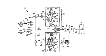
Figure 12 is a block diagram of another embodiment of
a non-coherent spread spectrum correlator using separable
real and imaginary parts of the received spread spectrum
signal. The Fig. 12 correlator uses only two shift
registers instead of four shift registers and uses only a
single power divider having no imposed phase delay for
operating on the received signal s*(t) as opposed to three
W096/08077 PCT~S9S/10886
.
O 2 1 9 9 5 2 5
32
power dividers in the non-coherent correlator illustrated
in Fig. 10. The use of a power divider having no imposed
phase delay on the received signal s*(t) is an advantage
because power dividers which impose a phase delay on the
typically operate optimally over only a relatively narrow
bandwidth, while the received signal may cover a
relatively wide bandwidth.
In Fig. 12, the received signal s*(t) 401 is coupled
to a two-register non-coherent CPM correlator 802 for
recognizing a chip sequence in the received signal s*(t).
The two-register non-coherent CPM correlator 802 comprises
a first power divider 803, which produ~es duplicate
signals 804 and 805, each with a 0-degree phase delay. A
local oscillator 806 produces a local carrier signal cos
w1t 807, which is coupled to a second power divider 808.
The second power divider 808 produces duplicate signals,
one signal 809 with a 0-degree phase delay, and another
signal 810 with a 90-degree phase delay. The use of the
second power divider 808 to generate signals cos ~1 and sin
~l from the same local oscillator 806 maintains the phase
offset o between ~l and ~0 for both cos ~1 and sin ~1.
The signals 804 and 809 are coupled to a first
multiplier 811, which combines its inputs and produces a
first product signal 812. The first product signal 812 is
coupled to a first low pass filter 813, which produces a
first filtered signal 814 which retains its baseband
frequency components. The first filtered signal 814 is
coupled to a first even-odd correlator 815.
The signals 805 and 810 are similarly coupled to a
second multiplier 816, which combines its inputs and
produces a second product signal 817. The second product
signal 817 is similarly coupled to a second low pass
filter 818, which produces a second filtered signal 819
which retains its baséband frequency components. The
second filtered signal 819 is similarly coupled to a
second even-odd correlator 820.
~--
W096l08077 PCT~S9511~886
~ 2 ~ 9 9 5 2 5
33
In the two-register non-coherent CPM correlator 802
depicted in Fig. 12, the Q portion of the Real*~t) signal
~ ls the same as the I portion of the Imag*(t) signal, and
the Q portion of the Imag*(t) signal is 180-degrees out of
phase (i.e., the inverse) of the I portion of the Real*(t)
signal. The Q portion of the Real*(t) signal and the I
portion of the Imag*(t) signal are stored in and read from
the same register 821. Similarly, the Q portion of the
Imag*(t) signal and the I portion of the Real*(t) signal
are stored in and read from the same register 827. The
two-register non-coherent CPM correlator 802 of Fig.`12
operates in a conceptually similar manner to the non-
coherent CPM correlator 702 of Fig. lO.
The first even-odd correlator 815 simultaneously
recognizes the real i*(t) components and the imaginary
q*(t) components, and comprises a register 821 capable of
holding a sequence of chips 822. The odd chips are
coupled to a real I summer 823, which combines its inputs
and produces a real I correlation signal 824. The even
chips are coupled to an imaginary Q summer 825, which
combines its inputs and produces an imaginary Q
correlation signal 826.
The second even-odd correlator 820 simultaneously
recognizes the imaginary i*(t) components and the real
q*(t) components, and comprises a register 827 capable of
holding a sequence of chips 828. The odd chips are
coupled to an imaginary I summer 829, which combines its
inputs and produces an imaginary I correlation signal 830.
The even chips are coupled to a real Q summer 831, which
combines its inputs and produces a real Q correlation
signal 832.
The real I correlation signal 824 and the real Q
correlation signal 832 are coupled to a real summer 833,
which combines its inputs and produce a real correlation
signal 834. Similarly, the imaginary Q correlation signal
826 and the imaginary I correlation signal 830 are coupled
W096/08077 PCT~S95110886
02 1 99 525
34
to an imaginary summer 835, which combines its inputs and
produces an imaginary correlation signal 836.
The real correlation signal 834 is coupled to a
squaring device 837, which computes the square of its
input. The imaginary correlation signal 836 is coupled to
a squaring device 838, which computes the square of its
input. The two squared values are coupled to a summer
839, which combines its inputs and produces a unified
correlation signal 840 representing the sum of the squares
of the real correlation signal 834 and the imaginary
correlation signal 836. The unified correlation signal
840 is coupled to a square root device 841 which ta~es the
square root of its input and generates a final carrelatio~
signal 842. The squaring devices 837 and 838, the summer
839, and the square root device 841 collectively compute
the root of the sum of the squares of the real and
imaginary signals. A Robertson device such as depicted in
Fig. 22 and described elsewhere herein may be used to
estimate the root of the sum of the squares. The time
between separate correlation pulses 843 may be one symbol
code time period Ts if CSK is used.
It should be noted that in the non-coherent CPM
correlator 702 of Fig. 10 and the two-register non-
coherent CPM correlator 802 of Fig. 12, the process of
squaring destroys polarity information.
Figure 13A is a block diagram of a spread spectrum
receiver using serial correlation.
The received signal s*(t) 401 is coupled to a
coherent serial CPM correlator 902 for recognizing a
correlation sequence in the received signal s*(t) 401.
The coherent serial CPM correlator 902 of Fig. 13A
comprises a power divider 903, which produces duplicate
signals 904 and 905 with a 0-degree phase delay. The
signal 904 is coupled to an I multiplier 906. The other
input of the I multiplier 906 is coupled to a locally
generated signal i(t) cos ~otl that is, the carrier signal
W096/08077 PCT~S95/10886
0 2 1 9 9 5 2 5
combined with the I chip sequence of the correlation
sequence. The signal 905 is coupled to a Q multiplier
~ 911, which is coupled to a locally generated signal q(t)
sin ~ot, that is, the carrier signal combined with the Q
chip sequence of the correlation sequence. The coherent
serial CPM correlator of Fig. 13A uses a coherent
reference signal having a frequency ~0.
The i(t) signal, which is the waveform representing
the I chip sequence, and the q(t) signal, which is the
waveform representing the Q chip sequence, each comprise
tri-valued return to zero (RZ) waveforms, that is, they
are ~1 to indicate a logical "1", -1 to indicate ~ log~cal
~0", and 0 to indicate no value, as shown in Fig. 13B.
The i(t) signal and the q(t) signal are offset by one chip
time from each other in the sense that the i(t) signal has
a value of +1 or -1 at each odd chip time but is 0 during
the even chip times, and the q(t) signal has a value of +1
or -l at each even chip time but is 0 during the odd chip
times.
The I multiplier 906 combines its inputs and produces
an I product signal 907. The I product signal 907 is
filtered by a low pass filter (not shown) and is coupled
to an I integrator 908, which integrates its input and
dumps the sum under control of a control input 909. The
I integrator 908 produces an I correlation signal 910.
The Q multiplier 911 combines its inputs and produces
a Q product signal 912. The Q product signal 912 is
filtered by a low pass filter (not shown) and coupled to
a Q integrator 913, which integrates its input and dumps
the sum under control of a control input 914. The Q
integrator 913 produces a Q correlation signal 915.
Because the i(t) signal and the q(t) signals are tri-
valued return to zero waveforms, only one of the
integrators 908, 913 changes value at a time.
The I correlation signal 910 and the Q correlation
signal 915 are coupled to a summer 916, which combines its
inputs and produces a unified correlation signal 917. The
W096/08077 PCT~S95/10~6
0~ 1 g9 525
unified correlation signal 917 increases progressively in
a stepwise fashion and reaches a m~xlmllm when full
.
correlation is achieved. If CSK is used, then the largest
of the unified correlation signals 917 for a plurality of
parallel coherent serial CPM correlators 902 over a given
symbol code time Ts may be used to identify the received
symbol code. The I and Q integrators 908, 913 hold their
values until instructed to dump.
To properly control the integrate and dump operation,
synchronization information is necessary. To accomplish
this, a parallel correlator may operate in conjunction
~ith one or more serial correla~ors to provide the
necessary timing information. In such an embodiment, a
transmitter may first transmit data (e.g., a preamble)
which is received by the parallel correlator. The
parallel correlator generates a correlation pulse when the
received data is recognized, which correlation pulse is
used to control the timing of the serial correlator or
correlators.
Figure 14 is a block diagram of a non-coherent spread
spectrum receiver using serial correlation for separable
real and imaginary parts of the received spread spectrum
signal.
`Conceptually, the non-coherent serial CPM correlator
of Fig. 14 operates in a similar fashion as the non-
coherent CPM correlator 702 of Fig. 10. The received
signal s*(t) 401 is coupled to a non-coherent serial CPM
correlator 1002 for recognizing a chip sequence in the
received signal s*(t) 401. The non-coherent serial CPM
correlator 1002 comprises a power divider 1003, which
produces duplicate signals, Real*(t) 1004 having a 0-
degree phase delay, and Imag*(t) 1005 having a 90-degree
phase delay. Real*(t) 1004 and Imag*(t) 1005 are the real
and imaginary parts of the received signal s*(t) 401.
The Real*(t) signal 1004 is coupled to a serial CPM
correlator 1020 which produces a real correlation signal
1006. The Imag*(t) signal 1005 is similarly coupled to a
P~ S/10886
W096/08077
.
37 021 99 525
second serial CPM correlator 1020 which produces an
imaginary correlation signal 1007.
~ Each serial CPM correlator 1020 comprises a power
divider (not shown) which receives an input signal and
S splits it into duplicate signals 1021 and 1022 with a 0-
degree phase delay. The signal 1021 is coupled to a first
I multiplier 1023. The other input of the first I
multiplier 1023 is coupled to a locally generated non-
coherent reference signal cos ~lt = cos (~0 ~ ~)t + 0 as
described earlier with reference to Fig. 10. The output
of the first I multiplier 1023 is coupled to an I low pass
filter 1027, the output of which is coupled to a second I
multiplier 1029. The other input of the second
multiplier 1029 is coupled to an i~t) signal 1031, which
is the waveform representing the I chip sequence (see
Figs. 13A and 13B). --
The signal 1022 is coupled to a first Q multiplier1024. The other input of the first Q multiplier 1024 is
coupled to a locally generated non-coherent reference
signal sin ~lt = sin (~0 + a~)t + e as described earlier
with reference to Fig. 10. The output of the first Q
multiplier 1024 is coupled to a Q low pass filter 1028,
the output of which is coupled to a second Q multiplier
1030. The other input of the second Q multiplier 1030 is
coupled to a q(t) signal 1032, which is the waveform
representing the Q chip sequence (see Figs. 13A and 13B).
The output of the second I multiplier 1029 is coupled
to an I integrator 1033, which integrates its input and
dumps the sum under control of a control input 1035. The
I integrator 1033 produces an I correlation signal 1037.
The output of the second Q multiplier 1030 is coupled
to a Q integrator 1034, which integrates its input and
dumps the sum under control of a control input 1036. The
Q integrator 1034 produces a Q correlation signal 1038.
The i(t) signal, which is the waveform representing
the I chip sequence, and the q(t) signal, which is the
waveform representing the Q chip sequence, each comprise
W096/08077 PCT~S95/10886
021 99 525
38
tri-valued return to zero (RZ) waveforms, that is, they
are +1 to indicate a logical "l", -l to indicate a logical
~o~, and o to indicate no value, as shown in Fig. 13B.
The i(t) signal and the q(t) signal are offset by one chip
time from each other in the sense that the i(t) signal has
a value of +1 or -1 at each odd chip time but is 0 during
the even chip times, and the q(t) signal has a value of +1
or -1 at each even chip time but is 0 during the odd chip
times. Because the i(t) signal and the q(t) signals are
tri-valued return to zero waveforms, only one of the
integrators 1035, 1036 changes value at a time. The I and
Q integrators 1035, 1036 hold t~eir val~es unti'
instructed to dump.
As noted with respect to Fig. 13A, synchronization
information necessary for controlling the integrate and
dump operation of the I and Q integrators 1035, 1036 may
be obtained from a parallel correlator receiving timing
information from a transmitted preamble in order to
generate a correlation pulse. The correlation pulse may
be used to control the timing of the serial correlator or
correlators. Other suitable methods of control are also
possible.
The I correlation signal 1037 and the Q correlation
signal 1038 are coupled to a summer 1039, which combines
its inputs and produces a unified correlation signal 1006.
The unified correlation signal 1006- increases
progressively in a stepwise fashion and reaches a maximum
when full correlation is achieved. As noted, the CPM
correlator 1020 receiving the Real*(t) signal 1004
produces a real correlation signal 1006, and the second
CPM correlator 1020 receiving the Imag*(t) signal 1005
produces an imaginary correlation signal 1007.
The real correlation signal 1006 is coupled to a
squaring device 1008, which computes the square of its
input. The imaginary correlation signal 1007 is coupled
to a squaring device 1009, which computes the square of
its input. The two squared values are coupled to a summer
-
W096l~8077 PCT~S95/10886
0 21 99 5 2 5
39
1010, which combines lts inputs and produces a unified
correlation signal 1011 representïng the sum of the
~ squares of the real correlation signal 1006 and the
imaginary correlation signal 1007. The unified
correlation signal 1011 is pro~ided to a square root
device 1012 which takes the square root of its input, and
generates a final correlation signal 1013. If CSK is
used, a m~; mllm correlation pulse 1014 may be achieved
once per symbol code time Ts. The squaring of the
correlation pulses causes loss of polarity information in
the final correlation signal 1013.
Figure 15A is a block diagram of another e.m.~odim~nt
of a non-coherent spread spectrum receiver using seriaI
correlation for separable real and imaginary parts of the
received spread spectrum signal.
The received signal s*(t) 401 is coupled to a dual-
integrator non-coherent serial CPM correlator 1102 for
recognizing a chip sequence in the received signal s*(t)
401. The dual-integrator non-coherent serial CPM
correlator 1102 comprises a first power divider 1103,
which produces duplicate signals 1104 and 1105, each with
a 0-degree phase delay. A local oscillator 1106 produces
a local carrier signal cos ~t 1107, which is coupled to a
second power divider 1108. The second power divider 1108
produces duplicate signals, one signal 1109 with a 0-
degree phase delay, and another signal 1110 with a 9o-
degree phase delay.
The signals 1104 and 1109 are coupled to a first
multiplier 1111, which combines its inputs and produces a
first product signal 1112. The first product signal 1112
~ is coupled to a first low pass filter 1113, which produces
a first filtered signal 1114 retaining its baseband
fre~uency components.
The signals 1105 and 1110 are coupled to a second
multiplier 1116, which combines its inputs and produces a
second product signal 1117. The second product signal
1117 is coupled to a second low pass filter 1118, which
W096/08077 PCT~S95110886
0 21 99 5 2 5
produces a second filtered signal 1119 retaining its
baseband frequency components.
In dual-integrator non-coherent serial CPM correlator
1102, the Q portion of the Real*(t) signal is the same as
the I portion of the Imag*(t) signal, and the Q portion of
the Imag*(t) signal is 180-degrees out of phase (i.e., the
inverse) of the I portion of the Real*(t) signal.
First filtered signal 1114 is coupled to a real I
multiplier 1121, which is also coupled to a locally
generated signal i(t), that is, the i(t) chip sequence of
the correlation sequence (see Fig. 13B). The real I
multiplier 1121 combines its inputs and produces a real I
product signal 1122.
The first filtered signal 1114 is also coupled to an
imaginary Q multiplier 1123, which is also coupled to a
locally generated signal q(t), that is, the in~erted q~t)
chip sequence of the correlation sequence (see Fig. 13B).
The imaginary Q multiplier 1123 combines its inputs and
produces an imaginary Q product signal 1124.
The second filtered signal 1119 is coupled to an
imaginary I multiplier 1125, which is also coupled to the
locally generated signal i(t). The imaginary I multiplier
1125 combines its inputs and produces an imaginary I
product signal 1126.
The second filtered signal 1119 is also coupled to a
real Q multiplier 1127, which is coupled to a locally
generated signal q(t), that is, the q(t) chip sequence of
the correlation sequence (see Fig. 13B). The real Q
multiplier 1127 combines its inputs and produce a real Q
product signal 1128.
The real I product signal 1122 and the real Q product
signal 1128 are coupled to a real summer 1129, which
combines its inputs and produces a real product signal
1130. The imaginary Q product signal 112~ and the
imaginary I product signal 1126 are coupled to an
imaginary summer 1131, which combines its inputs and
produces an imaginary product signal 1132.
W096t08077 P~ 5/l0886
.
O 2 1 99 5 2 5
41
The real product signal 1130 is coupled to a real
integrator 1133, which integrates its input and dumps the
sum under control of a control input 1134. The real
integrator 1133 produces a real correlation signal 1135.
The imaginary product signal 1132 is coupled to an
imaginary integrator 1136, which integrates its input and
dumps the sum under control of a control input 1137. The
imaginary integrator 1136 produces an imaginary
correlation signal 1138.
The real correlation signal 1135 is coupled to a real
squaring device 1139, which computes the square of its
input. The imaginary correlation signal 1138 is coupled
to an imaginary squaring device 1140, which computes the
square of its input. The two squared values are coupled
to a summer 1141, which combines its inputs and produces
a unified correlation signal 1142 which is the sum of the
squares of the real correlation signal 1135 and the
imaginary correlation signal 1136. The unified
correlation signal 1142 is coupled to a square root device
1143, which takes the square root of its input and
generates a final correlation signal 1144. The final
correlation signal 1144 may have a maximum value once per
symbol code time period Ts.
In a particular embodiment, a one-bit quantizor is
inserted at the output of the first low pass filter 1113
and the second low pass filter 1118.
In a preferred embodiment of the Fig. 15A correlator,
the real I multiplier 1121, imaginary Q multiplier 1123,
imaginary I multiplier 1125, and real Q multiplier 1127
3C each comprise an inverted XOR gate. Inverted XOR gates
are well known in the art; they have a truth table as
shown in the table below:
A B Inverted XORtA.B)
-1 -1 +1
-1 +1 -1
+ 1 - 1 - 1
+l +l +l
W096/08077 PCT~S9S/10886
0 2 1 9 9 5 2 5
42
In a preferred embodiment, the real summer 1129 and
real integrator 1133 collectively comprise a multiplexer
and integrator. Instead of computing the individual real
I and real Q components, summing them, and integrating the
sum, in a preferred embodiment the individual real I and
real Q components are multiplexed into a single stream and
the stream itself integrated.
Likewise, the imaginary summer 1131 and imaginary
integrator 1136 collectively comprise a multiplexer and
integrator. Instead of computing the individual imaginary
I and imaginary Q components, summing them, and
integrating the sum, in a preferred emkodiment the
individual imaginary I and imaginary Q components are
multiplexed into a single stream and the stream itself
integrated.
In a preferred embodiment, the first squaring device
1139, the se.cond squaring device 1140, the summer 1141,
and the square root device 1143 collectively comprise a
device using the Robertson technique for computing the
square root of the sum of two squares. In the Robertson
technique, which is known in the art, the norm.. of a plane
vector (the square root of the sum of two squares) having
coordinates cx,y~ may be approximated as follows:
¦~ cx,y, ll = m~;mllm(x~y) + (.5) m;n~ml~m(X,y
(1152)
A preferred embodiment of a Robertson device is shown
in Fig. 22 and is described later herein.
Figure 15B is a block diagram of a spread spectrum
receiver using multi-bit serial correlation for separable
real and imaginary parts of the received spread spectrum
signal. The Fig. 15B receiver comprises a first power
divider 1153 coupled to a received signal s*(t) 401, a
local oscillator 1156, a second power divider 1158,
multipliers 1161 and i166, and low pass filters 1163 and
1168, all of which are similar to the Fig. 15A embodiment.
Also like the Fig. 15A embodiment, the Q portion of the
Real*(t) signal is the same as the I portion of the
W096l08077 PCT~S95110886
` 02199 525
43
Imag*(t) signal, and the Q portion of the Imag*(t) signal
is 180-degrees out of phase (i.e., the inverse) of the I
portion of the Real*(t) signal.
The low pass filter 1163 is coupled to a two-bit
analog-to-digital (A/D) converter 1164, and the other low
pass filter 1168 is coupled to another two-bit A/D
converter 1169. The two-bit A/D converters 1164 and 1169
each quantize their respective input waveforms, and output
a two-bit pattern corresponding to the amplitude of the
input waveform. Figure 15C is a graph showing a two-bit
quantization of an input waveform 1154. Four amplitude
regions 1155 are depicted in the graph of Fig. 15~. When
the input waveform 1154 (e.g., the output of low pass
filter 1163 or 1168) is in the highest amplitude region
1155, the A/D converter 1164 or 1169 outputs a two-bit
pattern I1Io of 11. When the input waveform 115g is in the
next highest amplitude region 1155, the A/D converter 1164
or 1169 outputs a two-bit pattern IlIo of lO. Likewise, in
the next highest amplitude region 1155, the A/D converter
1164 or 1169 outputs a two-bit pattern IlIo of 01, and in
the lowest amplitude region 1155 the A/D converter 1164 or
1169 outputs a two-bit pattern I1Io of 00.
The inputs of A/D converters 1164, 1169 are sampled
once each chip period. The outputs 1165, 1170 of the A/D
converters 1164, 1169 are provided to a multi-bit non-
coherent serial correlation block 1167. The output 1165
of A/D converter 1164 is coupled to the input of a
multiplier 1172, which has another input coupled to a
locally generated i(n) chip signal, which, in a particular
30 embodiment, generates a two's complement waveform
corresponding to the tri-value return-to-zero waveform
used in Fig. 15A. The output 1165 of A/D converter 1164
r is also coupled to the input of a second multiplier 1174,
which has another input coupled to a locally generated
35 inverse q(n) chip signal, which is likewise a tri-valued
signal represented in two's complement format. The output
1170 of A/D converter 1169 is coupled to the input of a
W096/08077 PCT~S95/10886
0 2 1 9 9 5 2 5
multiplier 1171, which has another input coupled to the
i(n) chip signal. The output 1170 of A/D converter 1169
is also coupled to the input of another multiplier 1173,
which has another input coupled to a q(n) chip signal.
Each of multipliers 1171, 1172, 1173 and 1174 is
preferably embodied as a digital multiplier that
multiplies its inputs and generates a result in two's-
complement format. A preferred input and output truth
table for each of multipliers 1171, 1172, 1173 and 1174
appears in Table 15-1 below, wherein ic and qc represent
the chip value of the i(t) or q(t) signal at the
appropriate time interval. A binary 0-bit for ic or qc
represents a -1 chip value, while a binary l-bit for ic or
qc represents a +1 chip value. These values are, as noted
for this particular embodiment, expressed in two's
complement format for the signals i(n) and q(n).
Table 15-l
A/D Decimal
Output I/Q Signal Result Equiv-
20 (Il Io) (ic or a) (2 l O~ alent
0 o 0 0 1 0 +2
0 0 1 1 1 0 -2
0 1 0 0 0 0 +1
0 1 1 1 1 1 -1
25 l 0 0 1 1 1 -1
0 1 0 0 1 +1
1 1 0 l 1 0 -2
1 1 1 0 1 0 +2
The output from each of multipliers 1171, 1172, 1173
and 1174 comprises a 3-bit digital signal according to
Table 15-1. The outputs from multipliers 1171, 1172, 1173
and 1174 are coupled to accumulators 1175, 1176, 1177, and
1178, respectively. A chip clock signal 1181 is connected
to each of the accumulators 1175, 1176, 1777 and 1178, and
causes the accumulators 1175, 1176, 1177 and 1178 to
sample their inputs once each chip period. Thus, for a
W096t08077 PCT~S95/10886
45 0 2 1 9 9 5 2 5
symbol code length of 32 chips, the accumulators 1175,
1176, 1177 and 1178 sample their inputs 32 times for a
given symbol code. At each sample time, the accumulators
1175, 1176, 1177 and 1178 add the input to a running
correlation total. Because the outputs of A/D converters
1164 and 1169 are represented in two's-complement
notation, the accumulators 1175, 1176, 1177 and 1178
effectively carry out addition or subtraction by
performing only adding operations. A dump signal 1182
clears the accumulators at the end of each symbol period.
For a 32 chip symbol code, the running accumulator totals
will vary between +32 and -32.
Alternatively, instead of using the two's-complement
format signals i~n) and q~n), the tri-valued return-to-
zero waveforms such as i(t) and q(t) (see Fig. 15A) may beused. In such a case, the accumulators 1175, 1176, 1177
and 1178 would each accumulate every other clock cycle in
an alternating pattern, rather than every clock cycle.
Each accumulator 1175, 1176, 1177, and 1178 outputs
a 6-bit digital accumulation value. The outputs of
accumulators 1176 and 1177 are coupled to the inputs of a
first summer 1179. The outputs of accumulators 1175 and
1180 are coupled to the inputs of a second summer 1180.
Outputs of summers 1179 and 1180 are coupled to a
magnitude calculation block 1185 and a phase calculation
block 1187. The magnitude calculation block 1185 may be
embodied as a Robertson device (see, e.g., Fig. 22). The
phase calculation block 1187 may be embodied as, e.g., a
phase sector lookup table as shown in and described
elsewhere herein with respect to Fig. 25B. The magnitude
calculation block 1185 and phase calculation block 1187
output a unified correlation signal 1186 and a phase
signal 1188, respectively. The unified correlation signal
1186 may be, e.g., a 7-bit unsigned digital signal.
Expirement has shown that the correlator of Fig. 15B
can realize an improvement in bit error rate (BER) and
Eb/No (bit energy/noise density) of approximately 1.5 to
W096/08077 PCT~S95/10886
0 2 1 9 9 5 2 5
46
2.0 dB over the correlator of Fig. 15A. While two-bit
quantization leads to a significant improvement over
single-bit quantization, it is expected that higher order
quantization will yield increasingly smaller gains in BER
and Eb/No ratio up to a m~X; mllm aggregate improvement of
about 3 dB. Thus, two-bit quantization provides an
advantageous combination of improved performance without
a large increase in hardware complexity.
Figure 15D is a block diagram of a portion of another
embodiment of a spread spectrum receiver using multi-bit
serial correlation for separable real and imaginary parts
of the received spread spectrum signal. The circuitry
shown in Fis. 15D corresponds to the multi-bit non-
coherent serial correlation block 1167 depicted in Fig.
15B, but uses fewer components than the Fig. 15B
embodiment.
In Fig. 15D., signal 1165 (see Fig. 15B) and a c(t)
chip signal (i.e., a combined i(t) and q(t) signal) are
coupled to inputs of a first multiplier 1189. Signal 1170
(see Fig. 15B) and the c(t) chip signal are coupled to
inputs of a second multiplier 1190. Multipliers 1189 and
1190 each carry out arithmetic operations according to
Table 15-1. The output of the first multiplier 1189 is
coupled to the input of a multiplexer 1191, and is coupled
through an inverter 1193 to the input of another
multiplexer 1192. The output of the second multiplier
1190 is coupled to an input of each of multiplexers 1191
and 1192.
A multiplexer clock signal 1196 controls the
selection of inputs for each of multiplexers 1191 and
1192. Operation of multiplexer clock signal 1196 is based
on the recognition that the i(t) and q(t) chip signals are
staggered and will be zero every other chip time (see,
e.g., Fig. 13B). The multiplexer clock signal 1196 causes
the input of the multiplexers 1191, 1192 to switch so as
to ignore the output from the multiplier 1189, 1190 that
would be zero because the i(t) or q(t) portion of the ctt)
W096t08077 PCT~S95110886
.
O 21 99 5 2 5
47
chip signal is zero. Thus, the inputs to multiplexers
1191, 1192 are switched each chip time.
The output from multiplexer 1191 is input to an
accumulator 1194. The output from multiplexer 1192 is
input to another accumulator 119~. Accumulators 1194 and
1195 function similarly to accumulators 1175, 1176, 1177
or 1178 in Fig. 15B, by performing two's-complement
accumulation of their inputs to keep a running correlation
total. The accumulators 1194, 1195 are controlled by a
chip clock signal 1197 and a dump signal llg8, similar to
chip clock signal 1181 and dump signal 1182, respectively,
= .
of Fig. 15B.
The output 1260 of accumulator 1194 is coupled to a
magnitude calculation block 1262 and a phase calculation
block 1263. The output 1261 of accumulator 1195 is
likewise coupled to magnitude calculation block 1262 and
phase calculation block 1263. Magnitude calculation block
1262 is similar to magnitude calculation block 1185 of
Fig. 15B; phase calculation block 1187 is likewise similar
to phase calculation block 1187 of Fig. 15B. Magnitude
calculation block 1262 and phase calculation block 1263
output a. unified correlation signal 1264 and a phase
signal 1265, respectively.
A method of receiving and despreading a spread
2~ spectrum signal using non-coherent multi-bit serial
correlation is also provided. The method includes the
steps of dividing a spread spectrum signal into first and
second duplicate signals, demodulating the first signal
into a real-I/imaginary-Q signal using a first non-
coherent local reference signal, demodulating the secondsignal into an imaginary-I/real-Q signal using a second
non-coherent local reference signal having the same
frequency as said first non-coherent local reference
signal but phase offset therefrom by 90 degrees,
converting the real-I/ imaginary-Q signal into a first
multi-bit digital signal, converting the imaginary-I/real-
Q signal into a second multi-bit digital signal,
W096/08077 P~l/u~5/10886
0 2 1 g9 5 2 5
48
correlating the first multi-bit digital signal with a chip
sequence comprising odd chips and even chips, accumulating
a first correlation total, correlating the second multi-
bit digital signal with the odd chips and an inverse of
the even chips of the chip sequence, accumulating a second
correlation total, and combining the first correlation
total and the second correlation total to generate a
unified correlation output signal.
In one variation of the method, the steps of
correlating said first multi-bit digital signal,
accumulating a first correlation total, correlating said
second multi-bit digital signal, accllmulatirg a second
correlation total, and combining said first correlation
total and said second correlation total comprise the steps
of multiplying the real-I/imaginary-Q signal with said odd
chips to generate a real I product signal, multiplying the
imaginary-I/real-Q signal with said even chips to generate
a real Q product signal, multiplying the imaginary-I/real-
Q signal with said odd chips to generate an imaginary I
product signal, multiplying the real-I/imaginary-Q signal
with the inverse of said even chips to generate an
imaginary Q product signal, individually accumulating at
each chip period of said chip sequence the real I product
signal, real Q product signal, imaginary I product signal,
and imaginary Q product signal, summing the accumulated
real I product signal and the accumulated real Q product
signal into a real correlation signal, summing the
accumulated imaginary product signal and the accumulated
imaginary Q product signal into an imaginary correlation
signal, and combining the real correlation signal and the
imaginary correlation signal into a unified correlation
signal.
In another variation of the method, the steps of
correlating said first multi-bit digital signal,
accumulating a first correlation total, correlating said
second multi-bit digital signal, accumulating a second
correlation total, and combining said first correlation
w096/08077 PCT~S95/10~6
-- O 21 99 5 2 5
49
total and said second correlation total comprise the steps
of multiplying the real-I/imaginary-Q signal with the chip
sequence c(t) to generate a real-I/imaginary-Q product
signal, multiplying the imaginary-I/real-Q signal with the
chip sequence c(t) to generate an imaginary-I/real-Q
product signal, sampling and adding the real-I/imaginary-Q
product signal into a first running correlation total
(e.g., a real correlation total) the imaginary-I/real-Q
product signal into a second running correlation total
(e.g., an imaginary correlation total) for the odd chips
of the chip sequence, and sampling and adding the
imaginary-I/real-Q product signal into said first running
correlation total an inverse of the real-I/imaginary-Q
product signal into a second running correlation total for
the even chips of the chip sequence.
Figure 16 shows a block diagram of a first spread
spectrum receiver using self-synchronized correlation for
separable real and imaginary parts of the received spread
spectrum signal.
The received signal s*(t) 401 is coupled to a
self-synchronized CPM correlator 1202 for recognizing a
correlation sequence in the received signal s*(t) 401.
The self-synchronized CPM correlator 1202 comprises a
power divider 1203, which produces duplicate signals,
Real*(t) 1204 having a 0-degree phase delay, and Imag*(t)
1205 having a 90-degree phase delay. Real*(t) 1204 and
Imag*(t) 1205 are the real and imaginary parts of the
received signal s*(t) 401.
The Real*(t) signal 1204 is coupled to a real
correlator 1206, which divides its input signal by a power
divider (not shown) or other suitable means. The real
correlator 1206 comprises a real I multiplier 1207, which
is also coupled to a local carrier signal cos ~lt. The
real I multiplier combines its inputs and produces a real
I product 1208. The real I product 1208 is coupled to a
real I low pass filter 1209, which filters its input and
produces a filtered real I signal 1210.
W096t08077 PCT~S95/10886
0 2 1 9 9 5 2 5
The filtered real I signal 1210 is coupled to a real
I self-synchronizing correlator 1211, such as a correlator
using self-synchronizing techniques described in
Application Serial No. _ / (attorney docket
5 206/300) entitled 'IMethod and Apparatus for Despreading
Spread Spectrum Signals," filed May l, 1995 in the name of
inventors Robert Gold and Robert C. Dixon, which
application is assigned to the assignee of the present
invention and hereby incorporated by reference.
The real I self-synchronizing correlator 1211
comprises a shift register 1212 having a plurality of
chips 1213 and a plurality of taps 1214 ccupled to
selected chips 1213. The taps 1214 are coupled to a first
tap multiplier 1215, which combines its inputs to produce
15 a product which is thereafter coupled to a second tap
multiplier 1216. The second tap multiplier 1216 is also
coupled to the filtered real I signal 1210. The second
tap multiplier 1216 combines its inputs and produces a
real I correlation signal 1217.
The real correlator 1206 further comprises a real Q
multiplier 1218, which is coupled to a local carrier
signal sin wlt. The real Q multiplier 1218 combines its
inputs and produces a real Q product 1219. The real Q
product 1219 is coupled to a real Q low pass filter 1220,
25 which filters its input and produces a filtered real Q
signal 1221.
The filtered real Q signal 1221 is coupled to a real
Q self-synchronizing'correlator 1222, which produces a
real Q correlation signal 1223.
The Imag*(t) signal 1205 is coupled to an imaginary
correlator 1224, which divides its input signal by a power
divider (not shown) or other suitable means. The A
imaginary correlator 1224 comprises an imaginary
multiplier 1244, which is also coupled to a local carrier
signal cos w1t. The imaginary I multiplier 1244 combines
its input and produces an imaginary I product 1225. The
imaginary I product 1225 is coupled to an imaginary I low
W096l08077 PCT~S95/10886
0 21 99 5 2 5
51
pass'filter 1226, which filters its input and produces a
filtered imaginary I signal 1227. '
' The filtered imaginary I signal 1227 is coupled to an
imaginary I self-synchronizing correlator 1228, which
produces'an imaginary I correlation signal 1229.
The imaginary correlator 1224 comprises an imaginary
Q multiplier 1230, which is also coupled to a local
carrier signal sin ~lt. The imaginary Q multiplier 1230
combines its inputs and produces an imaginary Q product
1231. The imaginary Q product 1231 is coupled to an
imaginary Q low pass filter 1232, which filters its input
and produces a filtered imaginary Q signal 1233
The filterçd imaginary Q signal 1233 is coupled to an
imaginary Q self-synchronizing correlator 1234, which
produces an imaginary Q correlation signal 1235.
The real I correlation signal 1217 and the imaginary
I correl~tion signal 1229 are coupled to squaring devices
1236 an~ 1237 respectively, the outputs of which are
coupled to a summer 1238, to produce a unified
correlation signal 1239. The unified I correlation signal
1239 is coupled to a square root device 1250 which takes
the square root of its input and generates an final I
correlation signal 1251.
The real Q correlation signal 1223 and the imaginary
Q correlation signal 1235 are coupled to squaring devices
1240 and 1241 respectively, the outputs of which are
coupled to a summer 1242, to produce a unified Q
correlation signal 1243. The unified Q correlation signal
1243 is coupled to a square roo't device 1252 which takes
the square root of its input and generates an final Q
correlation signal 1253.
Embodiments and other aspects of the inventions
described herein, including the system embodiments
described below, may b'e made or used in conjunction with
inventions described, in whole or in part, in the patents,
publications, or copending applications referred to herein
as well as in copending U.S. Patent Application Serial No.
W096l08077 PCT~S95/10~6
0 2 1 9 9 5 2 5
~2
08/161,187, filed December 3, 1993 in the name of
inventors Robert C. Dixon and Jeffrey S. Vanderpool,
entitled "Method and Apparatus for Establishing Spread
Spectrum Communication," or copending U.S. Patent
Application Serial No. 08/284,053, filed August 1, 1994,
filed in the name of inventors Gary B. Anderson, Ryan N.
Jensen, Bryan K. Petch, and Peter O. Peterson, entitled
"PCS Pocket-Phone/ Microcell ~ommunication Over-Air
Protocol," both of which applications are hereby
incorporated by reference as if set forth fully herein.
Figure 17A is a block diagram of a preferred
transmitter.
In a preferred embodiment, a spread spectrum
transmitter 1337 operates in a cellular environment like
that described with respect to Fig. 2. The transmitter
1337 may be associated with either a base station or a
user station in such a cellular environment. In a
preferred embodiment, the transmitter 1337 operates
according to an over-air protocol for communication
betweer~ e base station and the user station, in which
transm:: _on is time-division duplex between the base
station and the user station in a single frame, and is
time-division multiplexed among multiple user stations in
a repeated pattern of frames. Other and further details
regarding a preferred over-air communication protocol may
be found in Application Serial Nos. 08/161,187 and
08/284,053 cited above. However, the present invention
will work in a variety of different communication
environments, cellular or otherwise, and according to a
variety of different protocols, whether or not such
protocols make use of time-division duplexing or time-
division multiplexing.
A preferred comml7n-cation protocol is depicted in
Fig. 17D. As shown ïn Fig. 17D, a polling loop 1380
("major frame") comprises a plurality of time slots 1381
("minor frames"). Each minor frame 1381 preferably
comprises communication between a base station (e.g.,
W096/08077 PCT~Ss5/10886
~ 0 2 1 99 5 2 5
53
cellular station) and a user station (e.g., mobile user)
in time division duplex -- that is, the base station
~ transmits to a user station and the user station transmits
back to the base station within the same minor frame 1381.
More specifically, as shown in an exploded view in
Fig. 17D, a minor frame 1381 preferably comprises a mobile
or user transmission 1382 preceding a base transmission
1383. The minor frame 1381 also comprises a variable
radio delay gap 1384 preceding the user transmission 1382,
followed by a turn-around gap 1388 and a guard time gap
1389. After gap 1389 is the base transmission 1383, which
is followed by another turn-around gap 1393. The user
transmission 1382 comprises a preamble 1385, a preamble
sounding gap 1386, and a user message interval 1387. The
base transmission comprises a preamble 1390, a preamble
sounding gap 1391, and a base message interval 1392.
Another communication protocol is shown in Fig. 17B.
While operation of the transmitter in Fig. 17A is
generally described with reference to the Fig. 17B
protocol, the same techniques may be applied for use with
the preferred protocol shown in Fig. 17D. In the
particular protocol of Fig. 17B, a polling loop 1301
(''major frame") comprises a plurality of time slots 1302
(~minor frames"). Each minor frame 1302 comprises
communication between a base station (e.g., cellular
station) and a user station (e.g., mobile user) in time
division duplex -- that is, the base station transmits to,
a user station and the user station transmits back to the
base station within the same minor frame 1302.
More specifically, as shown in an exploded view in
Fig. 17B, a minor ~rame 1302 comprises a power control
pulse transmission 1304 from the user station to the base
~ station, a base station transmission 130~, and a user
station transmission 1306, each of which is surrounded by
guard bands 1303. Details regarding the power control
pulse transmission 1304 may be found in Application Serial
No. 08/284,053, filed August 1, 1994, and incorporated
W096/08077 PCT~S95/10~6
021 99 525
54
herein by reference. The base station transmission 1305
and the user station transmission 1306 have a similar
structure; thus, the following description regarding the
base station transmission 1305 applies equally to the user
station transmission 1306.
The base station transmission 1305 comprises an
interframe gap 1351, a matched filter code 1352, a first
fill code 1353, a data sequence 1354, and a second fill
code 1355 similar to the first fill code 1353. The
interframe gap 1351 may be four chips in duration; the
matched filter code 1352 may be 48 chips duration; the
first fill code 1353 may be 16 chips in duration; the dat~
sequence 1354 may be comprised of one or more symbol
codes, each of which may be 32 chips, 128 chips, 2048
chips, or some other number of chips in duration depending
upon a data rate for transmission between the base station
and the user station; and the second fill code 1355 may be
a sufficient number of chips in duration to complete the
minor frame 1302. A plurality of minor frames 1302 may
comprise a channel.
The fill codes 1353, 1355 preferably each comprise a
code that has a low cross-correlation with each of the
symbol codes, and may form a repeated pattern such as "0
1 0 1 . . .'~ or "0 0 1 1 . . . ." The interframe gap 1351
may have the same code as one or both of the fill codes
1353, 1355. Fill codes 1353, 1355 are generated primarily
for the purpose of starting the modulator in a known state
at the beginning of a transmission, and to avoid having to
turn the transmitter off and on for the time period while
the fill code 1305 is transmitted. The fill codes 1353,
1355 may further be selected to improve the spectral
characteristics of the overall transmission.
The transmitter 1337 of Fig. 17A is a preferred means
for generating a base station transmission 1305 (or 1387
of Fig. 17D) or a user station transmission 1306 (or 1392
of Fig. 17D) using CPM techniques such as those described
elsewhere herein. A serial data stream 1321 of
W096/08077 PCT~S95/10886
0 2 1 9 9 5 2 5
information to be transmitted is provided to the
transmitter 1337 and converted to parallel data by a
serial-to-parallel shift register 1322. The parallel data
output by the serial-to-parallel shift register 1322 is
used to select from among a plurality of symbol codes
stored in a symbol code table 1323. Each symbol code, as
mentioned, is preferably 32 chips in length and represents
a predetermined number of data bits (preferably 5 data
bits) from the serial data stream 1321.
In addition to ~;toring various symbol codes in the
symbol code table 1323, the transmitter also comprises a
matched filter code generator 1324 capable of generating
a matched filter code 1352, and a fill code generator 1325
(which may be a table!) capable of generating fill codes
1353, 1355. The symbol code table 1323, matched filter
code generator 1324, and fill code generator 1325 are
selectively accessed by a control circuit 1320 for
constructing a transmission such as a base station
transmission 1305 or user station transmission 1306. A
transmission may be constructed, for example, by
concatenating or appending consecutive symbol codes, fill
codes, and other code sec~uences as necessary to generate
the appropriate chip secluence. Although connections are
not expressly shown, the control circuit 1320 has control
outputs 1339 connected to various parts of the circuit for
the purpose of exercising synchronous control.
In a preferred embodiment, timing information is
generated with a clock circuit 1307 such as a crystal
oscillator. The clock circuit 1307 produces a 20
megahertz (MXz) clock signal and is coupled to an input of
a clock chain 1308. The clock chain 1308 generates a
plurality of output clock signals in a manner known in the
- art. The clock chain :L308 has as outputs a 20 MHz clock
signal 1309, a 10 MHz clock signal 1310, a 5 MHz clock
signal 1311, and a 2.5 MHz clock signal 1312.
In a preferred e~odiment, the 5 MHz clock signal
1311 is coupled to a loop counter 1313, which, among other
W096/08077 PCT~S95/10886
.
O 2 1 9 9 5 2 5
56
things, counts chips over the course of each minor frame
1302. The loop counter ~313 produces a chip count signal
1314, a symbol count signal 1315, and a channel count
signal 1316. The channel or loop count signal 1316
5 indicates which minor frame 1302 is active within the
polling loop 1301. Thus, if there are 32 minor frames
1302 in a polling loop 1301, the channel count signal 1316
counts from O to 31 and then resets. When the channel
count signal 1316 indicates an active minor frame 1302 in
which the transmitter 1337 is authorized to transmit, the
control circuit 1320 may issue co~m~n~ to transmit
information at the appropriate time.
The symbol count signal 1315 keeps track of how many
symbols have been transmitted by the transmitter 1337 in
the data sequence 1354. Thus, if the transmitter is to
transmit 16 consecutive symbols as part of the data
sequence 1354, then the symbol count signal 1315 counts
from o to 15 and then resets.
The chip count signal 1314 keeps track of how many
20 chips have been transmitted by the transmitter 1337 for
the current symbol in the data sequence 1354. Thus, if
each symbol code is 32 chips in length, the chip count
signal 1314 counts from O to 31 and then resets. The chip
count signal 1314 also provides timing information for
25 those circuits in the transmitter which are clocked at
each chip time Tc.
The chip count signal 1314, the symbol count signal
1315, and the channel count signal 1316 are coupled to a
state decoder 1317, which determines whether the current
30 chip is part of the matched filter code 1352, the fill
code 1305, or a data sequence symbol code 1306, and which
generates a selection signal 1318 and a set of control
signals 1319. The control signals 1319 are coupled to a
control circuit 1320.
As mentioned, a serial data stream 1321 of data to be
transmitted is coupled to a serial-to-parallel shift
register 1322, which converts the serial data stream 1321
W096l08077 P~liu~g~l10~6
5 0 2 1 9 9 5 2 5
to a sequence of 5-b.it parallel symbols. The sequence of
symbols is coupled to an input of a symbol code table
i323, which selects f.or each symbol a specific symbol code
unique to the symbol.
The chip count signal 1314 is coupled to the symbol
code table 1323, the matched filter code generator 1324,
and the fill code generator 1325. Outputs of the symbol
code table 1323, the matched filter code generator 1324,
and the fill code gen.erator 1325 are coupled to inputs of
a 3-1 multiplexor 1326. A control input of the 3-1
multiplexor 1326 is coupled to the selection signal 1318
from the control circuit 1320. The 3-1 multiplexcr 1326
thus generates an output chip stream 1327 in accordance
with the co~m~n~.~ provided by the control circuit 1320.
Specifically, the control circuit 1320 may select a fill
code to fill the interframe gap 1351 from the fill code
generator 1325, a matched filter code 1352 from the
matched filter code ge.nerator 1324, a first fill code 1353
from the fill code generator 1325, one or more symbol
codes (depending on the amount of data to be transmitted
and the data rate) corresponding to the data sequence 1354
from the symbol code table 1323, and a second fill code
1355 from the fill code generator 1325, in order to
construct a transmission such as a base station
transmission 1305 or a user station transmission 1306.
The output chip stream 1327 is coupled to a
demultiplexor 1328, which separates its input chip stream
into an I chip stream ~.329 and a Q chip stream 1330, under
control of the 2.5 ~z clock signal 1312 (i.e., the
demultiplexor 1328 is clocked at half the chip rate Rc).
The I chip stream 1329 and the Q chip stream 1330 are
connected to a wavefo;rm generator 1338 which generally
constructs appropriate output waveforms based on the
contents of the I chip stream 1329 and the Q chip stream
1330.
The waveform generator 1338 comprises an I lookup
table 1332 and a Q lookup table 1334, each of which
W096/08077 PCT~S9Sl10~6
0 21 99 5 2 5 -
58
comprises memory such as ROM. The I lookup table 1332 and
the Q lookup table 1334 each contain fifteen digitized
values for amplitude outputs of the P(t) devices 305 (for
I) and 306 (for Q) shown in Fig. 6. Thus, by changing the
contents of the lookup tables 1332, 1334 appropriately,
the shape of the output waveforms may be suitably altered,
allowing transmission of MSK, SQAM, GMSK, SQORC, or other
similar format as desired.
The I lookup table 1332 receives as its inputs both
the present I chip from the I chip stream 1329 and the
previous I chip from the I chip stream 1329 as stored in
an I delay element 1331 (e.g., a la~ch) By having
available the immediate past I chip and the present I
chip, the transmitter knows what type of transition is
occurring in the I chip stream 1329 -- that is, whether
the I chip stream 1329 is undergoing a 0/0 transition, a
0/1 transition, a 1/0 transition, or a 1/1 transition.
The type of transition determines the shape of the output
waveform. The I lookup table 1332 provides as output
eight sequential I waveform comm~n~.~ or "samples~ per I
chip time (i.e., 2Tc) which are connected to a digital-to-
analog converter (DAC) for constructing a suitable
waveform. The I lookup table 1332 is provided a clock
input of 20 MHz so that eight I waveform comm~n~ may be
output per I chip time. In the transmitter 1337 shown in
Fig. 17, the DAC for the I chip stream 1329 comprises a 4-
15 decoder 1335 which selects one of 15 possible output
lines, coupled to a resistor ladder (not shown) and a low
pass filter (not shown). Of course, other types of DAC's
would be suitable for this purpose.
Table 17-1 below shows an example of how the 15
outputs of the 4-15 decoder 1335 relate to specific
voltages to be output by the DAC to create a SQAM waveform
varying between 1.5 V and 3.5 V:
W096/08077 PCT~S95/10886
59 0 2 1 99 5 2 5
Table 17-1
Decoder (Hex) Output AmPlitude (V)
0 1.5
1 1.5674
2 1.700
3 1.8414
4 1.900
3.100
6 3.1586
7 3.300
8 3.4326
9 3.500
A 3.2071
B 2.8827
C 2.500
D 2.1173
E 1.7929
Table 17-2 below shows a sequence of eight selected
values according to Table 17-l for constructing an
appropriate waveform depending on what type of transition
is occurring in the I chip stream:
Table 17-2
Transition Decoder OUtPUt Seauence
0 -~ 0 0, 1, 2, 3, 4, 3, 2, 1
0 -> 1 0, 1, E, D, C, B, A, 8
1 -~ 0 9, 8, A, B, C, D, E, 1
1 -~ 1 9, 8, 7, 6, 5, 6, 7, 8
An output corresponding to the Q chip stream 1330 is
generated in a similar manner to that of the I chip stream
1329. The Q lookup table 1334 receives as its inputs both
the present Q chip from the Q chip stream 1330 and the
previous Q chip from the Q chip stream 1330 as stored in
a Q delay element 1333. Based on its inputs, the Q lookup
table 1334 determines what type of transition is occurring
in the Q chip stream 1330. An output of the Q lookup
table 1334 is coupled to a 4-15 decoder 1336, which
selects one of 15 output lines for sending a signal to a
W096/08077 PCT~S9S/10~6
0 2 1 9 9 5 2 5
DAC configured in a similar manner to that described with
respect to the I chip stream 1329.
Thus, the contents of the I lookup table 1332 and the
Q lookup table 1334 are selected to generate an i(t)
output waveform and a q(t) output waveform, respectively.
An example of an output SQAM waveform 1370 according to
the technique described above and the values set forth in
Tables 17-1 and 17-2 is shown in Fig. 17C. The waveform
1370 comprises a 0/0 transition 1372, a 0/1 transition
1373, and a 1/1 transition 1374. Each transition 1372,
1373, 1374 comprises eight discrete points 1371
corresponding to values selected by the ~-15 I loQkup
table 1332 (or Q lookup table 1334). The effect of the
low pass filter (not shown) at the output of the waveform
generator 1338 smooths the shape of the waveform 1370
between discrete points 1371.
Table 17-3 shows an illustrative matched filter code
1352. In a presently preferred embodiment, the matched
filter code generator 1324 is configured to generate the
code shown below in Table 17-3.
Table 17-3
Hexadecimal Value Binarv Value
01000000
3E 00111110
34 00110100
B3 10110011
lA 00011010
A6 10100110
Selection of a matched filter code 1352 for a particular
application depends on the symbol codes (in a CSK system)
or other chip codes being used; generally, the matched
filter code 1352 is selected for low cross correlation
with the other chip codes used in the particular
communication environment.
Table 17-4 shows a presently preferred set of 32
symbol codes. In a preferred embodiment, the symbol code
table 1323 along with the appropriate comm~n~ from the
-
W096/08077 PCT~S95110~6
02199525
61
control circuit 1320 are configured to generate a sequence
of symbol codes selected from the set of 32 symbol codes
shown in Table 17-4, in response to a sequence of 5-bit
parallel symbols.
5 Table 17-4
Svmbol Symbol Code (Hex) ~vmbol Svmbol Code (Hex~
oo 0544D65E 10 OE4424Al
01 5Bl18EOB 11 5B1171F4
02 3D77E66D 12 3D771792
03 6822BD36 13 682242C7
04 014BD451 14 014B2BAE
Q5 541E8104 15 5~1E7EFB
06 3278E762 16 3278189D
07 672DB237 17 672D4DC8
08 OEBBDBAl lB OEBB245E
09 5BEE8EF4 19 5BEE71~B
OA 3D88E892 lA 3D86176D
OB 68DDBDC7 lB 68DD4238
OC OlB4D4AE lC OlB42B51
OD 54El81FB lD 54E17ED4
OE 3287E79D lE 32671862
OF 67D2B2C8 lF 67D24D37
Figures 18, 19, 21A and 21B collectively illustrate
a preferred receiver.
2~ The illustrated receiver generally operates by
correlating to a preceding spread spectrum code (e.g.,
matched filter code 1352 of Fig. 17B, or pream~le 1385 or
1390 shown in Fig. 17D) with a non-coherent parallel
correlator (such as the two-register non-coherent CPM
correlator 802 depicted in Fig. 12) to achieve
synchronization for a plurality of serial correlators
~such as the dual-integrator non-coherent serial CPM
correlators 110~ depicted in Fig. 15A). The serial CPM
correlators are then used for correlating to a following
message (e.g., data sequence 1354 of Fig. 17B, or messages
contained in the user message interval 1387 or base
message interval 1392 of Fig. 17D). However, many
W096/~8077 PCT~S95/10886
0 2 1 99 5 2 5
62
alternate configurations using, for example, only parallel
correlators, only serial correlators, or various
combinations of parallel and serial correlators, may be
used in the receiver without departing from the scope and
spirit of the invention. In a preferred embodiment, the
multi-bit serial correlators of Fig. 15B or 15D are used
for the plurality of serial correlators.
A preferred embodiment of a receiver is shown in part
in Figs. 21A and 21B. Standard electrical engineering
symbols and terms are used in Figs. 21A and 21B; thus, the
following explanation will be limited to relating Figs.
21A and 21B to the prior description of the inventior. in
some its various embodiments.
A received signal 2001 is provided to an IF amplifier
shown in Fig. 21A. The received signal 2001 may undergo
prior conditioning and may be downconverted to an
intermediate frequency for processing. The received
signal 2001 is coupled to a capacitor C4 which passes the
high frequency components of the received signal 2001.
The output of the capacitor C4 is coupled to a first
integrated chip U1 which is preferably an MC13155 chip
manufactured by Motorola. Specificaliy, the output of
capacitor C4 is coupled to a hardlimit amplifier 2003
located on the first integrated chip U1 for hardlimiting
the output of capacitor C4. The hardlimit amplifier
provides a differential output comprising a first
differential output signal 2010 and a second differential
output signal 2011.
The differential output signals 2010, 2011 are
coupled to a second integrated circuit U2 which, as shown
in Fig. 21B, is preferably an RF2701 chip manufactured by
RF Micro Devices. Specifically, the differential output
signals 2010, 2011 are coupled to a differential amplifier
2033 which produces an amplified output signal 2030. The
amplified output signal 2030 is split into two branches by
a power divider (not shown) and coupled via a first branch
to a first multiplier 2031 (e.g., multiplier 1111 in Fig.
W096/08077 PCT~S95110886
021 99 525
63
15A) and via a second branch to a second multiplier 2032
(e.g., multiplier 1116 in Fig. 15A). The first multiplier
2031 has as a second input a reference signal 2036
comprising a first square wave of frequency ~lt (which,
5 after low pass filtering, becomes cos ~t), and the second
multiplier 2032 has as another input a reference signal
2037 comprising a second square wave of frequency ~1t
(which, after low pass filtering, becomes sin ~lt) phase
offset from the first square wave by 90 degrees.
The reference signals 2Q36, 2037 are generated from
a local oscillator (not shown) which provides a local
oscillator signal 2025 to filter capacitQr C39, the output
of which is co~nected to the second integrated chip U2.
Specifically, the output of capacitor C39 is connected to
15 an amplifier 2038, the output of which is coupled to a
quad divide-by-two circuit 2039 for splitting its input
into two reference signals 2036, 2037, the first reference
signal 2036 having a 0-degree delay and the second
reference signal 2037 having a 90-degree delay. The
20 outputs of multipliers 2031 and 2032 are amplified by a
first output amplifier 2034 and a second output amplifier
2035, respectively.
The output of the first output amplifier 2034 is
coupled to a first low pass filter 2023, and the output of
25 the second output amplifier 2035 is coupled to a second
low pass filter 2024. The output of the first low pass
filter 2023 iS connected to one input of a first
comparator 2027. The output of the second low pass filter
2024 iS connected to one input of a second comparator
30 2040. The first comparator 2027 and second comparator
2040 each have as a second input a DC threshold signal
2041 generated by a DC bias circuit 2022. The DC
~ threshold signal 2041 iS coupled to the first comparator
2027 by a low pass filter comprising capacitor C52 and
35 resistor R36, and similarly to the second comparator 2040
by a low pass filter comprising capacitor C53 and resistor
R37. The first comparator 2027 and second comparator 2040
W096/08077 PCT~S95/10886
0 2 1 99 5 2 5
64
provide output signals 2028 and 2029, respecti~ely, each
of which comprises a TTL level signal suitable for further
processing using digital circuits. In particular, output
signals 2028 and 2029 may each comprise a square wave
signal having values of +1 and 0 times a fixed voltage.
In a preferred embodiment, the output signals 2028
and 2029 are sampled and provided to remaining circuitry
as shown in Figs. 18 and 19. Specifically, the output
signals 2028 and 2029 are sampled twice per chip time
(i.e., at 10 MHz) as provided to the circuitry in Fig. 18,
and once per chip time (i.e., at 5 MHz) as provided to the
circuitry in Fig. 19.
Figure 18 is a block diagram of a noncoherent matched
filter and associated receiver components.
In a preferred embodiment, a digitally sampied
version of a real portion and an imaginary portion of the
received signal s*(t) 401 are input to the circuitry of
Fig. 18. Thus, a real-I/ imaginary-Q signal 1401 is
connected to signal 2028 shown in Fig. 21B, and input to
an even/odd shift register 1402. ~l imaginary- I/real-Q
signal 1451 is connected to signal 2029 shown in Fig. 21B,
and input to an even/odd shift register 1452.
In the Fig. 18 embodiment, the even/odd shift
register 1402 is 96 bits long. ~ecause the real-
I/imaginary-Q signal 1401 is clocked at twice the system
clock rate, every other odd chip (rather than every odd
chip) of the even/odd shift register 1402 is selected and
compared with the odd chips of the matched filter code
1403. In a preferred embodiment, matches between every
other odd chip of the even/odd shift register 1402 and the
odd chips of the matched filter code are compared. The
chip matches are coupled to real adder 1404 for counting.
Every other even chip (rather than every even chip) of the
even/odd shift register 1402 is compared with the even
chips of the matched filter code 1403, and the result of
the comparison coupled to the imaginary adder 1405 for
counting.
W096/08077 PCT~S95tlOW6
-
0 2 1 9 9 5 2 5
In the Fig. 18 embodiment, the even/odd shift
register 1452 is 96 bits long. Every other odd chip of
the even/odd shift register 1452 is compared with the odd
chips of the matched filter code 1403. Matches between
every other odd chip of the even/odd shift register 1452
and the odd chips of the matched filter code are compared.
The chip matches are coupled to the real adder 1404 for
counting. Every other even chip of the even/odd shift
register 1452 is compared with the even chips of the
matched filter code 1403, and coupled to the imaginary
adder 1405 for counting.
Although the Fiq. 18 embodiment is configured to
receive a preamble 48 chips in length, in a preferred
embodiment the Fig. 18 receiver is configured to receive
a preamble of 128 chips in length, in accordance with the
preferred Fig. 17D message format. In this latter
embodiment, the even/odd shift register 1402 and the
odd/even register 1452 are each 256 bits long, and the
related circuitry is scaled up appropriately.
In the Fig. 18 embodiment, the real adder 1404 has 24
individual bit inputs, each one of which may be a logical
~O~ to indicate no match or a logical "1" to indicate a
match. The real adder 1404 generates a 5-bit real sum
1406, which represents the absolute value of the number of
2~ odd chips that were matched. The imaginary adder 1405 has
24 individual bit inputs and generates a 5-bit imaginary
sum 1407 representing the absolute value of the number of
even chips that were matched.
The real sum 1406 and the imaginary sum 1407 are
coupled to a Robertson device 1408, which computes an
approximation of a square root of the sum of the squares
of the real sum 1406 and the imaginary sum 1407, as
described herein.
An output of the Robertson device 1408 is coupled to
an input of a comparator 1409, which compares the output
of the Robertson device 1408 with a threshold value 1410.
In a preferred embodiment, the threshold value is preset,
W096/08077 PCT~S95/10~6
0 21 99 5 2 5
66
or may be set in response to a control on the receiver.
The threshold value may also be set in a variety of other
manners, such as in response to a control in the
transmission or to receiving conditions.
A comparator 1409 generates an output pulse 1411.
The output pulse is a logical "1" when the input 1430
exceeds the threshold 1410, and a logical "0" when it does
not. The output pulse 1411 may have a duration of 100,
200, 300 or 400 nanoseconds.
lo The output pulse 1411 is coupled to an input of a
center seeking detector circuit 1412. The center see~ing
detector circuit 1412 receives the output pulse 1411 and
generates a set clock pulse 1413 which denotes the end of
the received matched filter code 1352, and which is
aligned with the center of a received chip so that the
receiver clock can be synchronized with the cent-er of each
received chip in a received chip stream.
In a preferred embodiment, the center seeking
detector circuit 1412 counts the number of logic "1"
values in the output pulse 1411 (i.e., the length of time
that the output of the Robertson device 1408 exceeds the
threshold value 1410), thereby measuring the duration of
the output pulse 1411 (e.g., from 1 to 4 clock periods of
the 10 MHz clock, corresponding to up to four bits of the
even/odd shift register 1402 and the even/odd shift
register 1452). The center seeking detector-circuit 1412
generates a set clock pulse 1413 which re-initializes a
system clock for serial correlation by a set of serial
correlators (see Fig. 19) after a preset delay period.
The preset delay period ensures that the serial
correlation clock is properly synchronized with the center
of the output pulse 1411. Preferred delay periods are
shown in Table 18-1:
W096/08077 ~CT~S95/10886
0 21 99 5 2 5
67
Table 18-1
Lenqth of OutPUt Pulse DelaY in Nanoseconds
1 50
2 100
150
4 200
The system clock may be re-initialized at the start of
each minor frame 1302.
The set clock pulse 1413 is coupled to a clock chain
10 1415, which is also coupled to a locally generated 40 MHz
clock signal 1416. The clock chain 1415 generates a 20
MHz clock signal 1417, a 10 MHz clock signal '418, and a
5 MHz clock signal 1419. In a preferred embodiment, the
5 MHz clock signal 1419 is coupled to, among other things,
a set of 32 serial correlators (see Fig. 19).
The 5 MHz clock signal 1419 is coupled-to a loop
counter 1420. The loop counter 1420 counts the number of
chips received and generates a chip count signal 1421, a
symbol count signal 1422, and a channel or loop count
signal 1423, similar to the chip count signal 1314, symbol
count signal 1315, and channel count signal 1316,
respectively, generated in the transmitter 1337.
The chip count signal 1421, symbol count signal 1422,
and channel count signal 1423 are coupled to a state
decoder 1424, which determines whether the received chip
is part of the matched filter code 1352, the fill code
1305, or a data sequence symbol code 1306, similar to the
state decoder 1317 in the transmitter 1337, and generates
a state identifier 1425, similar to the selection signal
30 1318 generated in the transmitter 1337. The state
identifier 1425 is coupled to an input of the center
seeking detector circuit 1412.
~ The state decoder 1424 generates a synchronization
signal 1426, which is coupled to a set of 32 serial
35 correlators (see Fig. 19). The state decoder 1424 also
generates a plurality of control signals 1427, which are
coupled to a control circuit 1428. Although connections
W096t08077 PCT~S95/10886
0 2 1 99 5 2 5
68
are not expressly shown, the control circuit 1428 has
control outputs 1429 connected to ~arious parts of the
circuit for the purpose of exercising synchronous control.
The center seeking detector circuit 1412 also
5 generates a set state signal 1414 which may be used to
place the loop counter 1420 in a known state, or to reset
the individual count signals 1421, 1422 and 1423
associated with the loop counter 1420.
Operation of the center seeking circuit 1412 in
relation to the other elements shown in Fig. 18 may be
further explained with reference to Fig. 20, which is a
diagram of a series of correlation pulses 2007, 2011,
2012, 2013 and 2014 corresponding to output pulse 1411
over a series of minor frames 1302. A first correlation
pulse 2007 iS detected as shown in Fig. 18. The first
correlation pulse 2007 has a duration of three sample
periods 2008. Thus, according to Table 18-1, the center
seeking circuit 1412 generates a set clock pulse 1413
having a delay of 1~0 nanoseconds.
The control circuit 1428 determines, based in part on
the count signals 1421 through 1423 of the loop counter
1420, the next minor frame 1302 in which the receiver is
to be active. In many cases, a receiver receives in only
one minor frame 1302 per major frame 1301 located in the
25 same relative position chronologically from major frame
1301 to major frame 1301. Thus, in the next active minor
frame 1302, the receiver opens a timing window 2010 during
which the next output pulse 1411 iS expected. The timing
window may be, for example, 1.6 milliseconds in duration,
and will be opened a predetermined time length 2009 before
the next output pulse 1411 is expected assuming no
deviation between the transmitter and receiver clocks
between transmissions.
In the example of Fig. 20, a second correlation pulse
35 2011 iS generated during the timing window 2010 but some
amount of time after expected. The second correlation
pulse 2011 is two sample periods in duration, and thus,
W096l08077 PCT~S95/10886
O 2 1 9 9 5 2 5
according to Table 18-1, the center seeking circuit 1412
generates a set clock pulse 1413 having a delay of 100
nanoseconds. In the following active minor frame 1302,
the timing window 2010 has been shifted in relative time
~ased upon the second correlation pulse 2011, and a third
correlation pulse 2012 is generated within the timing
window 2010 but some amount of time before expected. The
third correlation pulse 2012 is four sample periods in
duration and causes a set clock pulse 1413 having a delay
of 200 nanoseconds.
Similarly, a fourth correlation pulse 2013 and fifth
correlation pulse 2014 are generated in the next two
active minor frames 1302. However, in the next active
minor frame 1302 no correlation pulse is generated; thus,
the receiver rem~; ns inactive because synchronization has
not been achieved. Measures may be undertaken at such a
point to reac~uire synchronization and/or re-establish
proper tlmlng.
Figure 19 is a block diagram of a preferred system of
serial correlators operating in parallel with one another
and operating in conjunction with the circuitry of Fig. 18
and Figs. 21A and 21B.
A digitally sampled version of a real portion and an
imaginary portion of the received signal s*(t) 401 are
input to the circuitry of Fig. 19. Thus, a real-
I/imaginary-Q signal 1511 and an imaginary-I/real-Q
signal 1512 are generated from the received signal s*(t)
401.
In a preferred embodiment; the 5 MHz clock signal
1419 and the synchronization signal 1426 as described in
Fig. 18 are coupled to a count chain 1501, which generates
an output synchronization signal 1502 for the serial
correlators and a counter clock 1503.
The 5 MHz clock signal 1419, the synchronization
signal 1502, the counter clock 1503, the real-I/imaginary-
Q signal 1511 and the imaginary-I/real-Q signal 1512 are
each coupled to a set of 32 serial correlators 1504. A
W096l08077 PCT~S95/10886
.
O 2 1 9 9 5 2 5
set of 32 symbol generators 1505, one for each symbol 00
through lF (hexadecimal), are also coupled to each serial
correlator 1504.
Each serial correlator 1504 recognizes a single one
of the 32 symbol codes and generates a magnitude signal
1506 indicating the number of agreements with that symbol
code. The 32 magnitude signals 1506 are coupled to a
best-of-M device 1507, which determines which one of the
32 magnitude signals 1506 has the greatest value and
generates an output symbol 1508 based thereon. If serial
output data is desired, the output symbol 1508 may be
_ coupled to a ~parallel-to-serial shift register 1509, which
generates a sequence of serial data bits 151Q in response.
An exploded view of an individual serial correlator
1504 is also shown in Fig. 19. The serial correlator 1504
shown in the Fig. 19 embodiment operates in a conceptually
similar manner to the dual-integrator non-coherent serial
CPM correlator 1102 depicted in Fig. 15A. In an
alternative preferred embodiment, the 32 serial
correlators operate according to the correlator
embodiments described with respect to Fig. 15B or 15D.
In a preferred embodiment, the real-I/imaginary-Q
signal 1511 is coupled to XNOR gates 1551 and 1552, and
the imaginary-I/real-Q signal 1512 is coupled to XNOR gate
1552. XNOR gates generate the inverted XOR of their
inputs. The XNOR gates 1551 and 1552 perform-the function
of multipliers 1121, 1123, 1125 and 1127 depicted in Fig.
15A. Each serial correlator 1504 is programmed to
correlate to a different symbol code; accordingly, the
appropriate symbol code is clocked into the XNOR gates
1551, 1552 and 1554 from the symbol generator 1505. The
symbol code is inverted by invertor 1553 before being
received by XNOR gate 1554 because XNOR gate 1554 operates
on the inverse of the q(t) signal.
Summation and integration is carried out by a pair of
multiplexors 1555, 1556 and counters 1557, 1558. The
outputs of the XNOR gates 1551 and 1552 are coupled to an
PCT~S95110886
W096/08077
0 2 1 9 9 5 2 5
71
real multiplexor 1555i the outputs of the XNOR gates 1552
and 1554 are coupled to an imaginary multiplexor 1556.
The counter clock 1503 is coupled to a control input of
the real multiplexor 1555 and the imaginary multiplexor
1556 in order to control the integrate-and-dump function.
The outputs of the real multiplexor 1555 and the imaginary
multiplexor 1556 are coupled to the enable inputs of the
real counter 1557 and the imaginary counter 1558,
respectively. Because the received I and Q signals are
time staggered, the real multiplexor 1555 selects between
real I and real Q signals and provides them to the real
counter 1557 to effectively sum and integrate the real I
and real Q signals; the imaginary multiplexor 1556 and
imaginary counter 1558 operate in an analogous manner with
respect to imaginary I and imaginary Q signals.
A reset command may be provided to the real counter
1557 and the imaginary counter 1558 to perform an
operation analogous to a "dump" as would be carried out
with integrate-and-dump circuits shown in Fig. 15A.
The output of the real counter 1557 and of the
imagina-y counter 1558 are coupled to a Robertson device
1559, which computes an approximation to the root of the
sum of the squares of its inputs. An output of the
Robertson device 1559 is output from the serial correlator
1504, and generally corresponds to the final correlation
signal 1144 such as described with respect to Fig. 15A.
A serial correlator 1504 may be designed to operate
with multi-bit resolution to improve correlation accuracy.
Figure 22 is a block diagram showing a preferred
embodiment of a Robertson device 16Ql.
The Robertson device 1601 has an input 1602 and an
input 1603, and computes an approximation of the square
root of the sum of the squares of its inputs, as shown in
equation 1152. The input 1602 and input 1603 may be
binary inputs such as 5-bit binary numbers. The input
1602 and the input 1603 are coupled to a comparator 1604,
W096/08077 PCT~S95/10886
0 2 1 9 9 5 2 5
72
which generates a control output 1605 indicating whether
the input 1602 is greater than the input 1603.
The input 1602 and the input 1603 are also coupled to
a selector 1606, which outputs the greater of the input
1602 and the input 1603 in response to the control output
605.
The input 1602 and the input 1603 are also coupled to
a selector 1607, which outputs the lesser of the input
1602 and the input 1603 in response to an inverse of the
control output 1605.
The output of the selector 1606 and the output of the
selector 1607 are coupled to an adder lÇ08. However,
prior to being connected to the adder 1608, the output of
the second selector 1607 is shifted right one bit, i.e.,
the 0 (least significant) bit of the output of the second
selector 1607 may be discarded, the 1 (next least
significant) bit of the output of the second selector 1607
may be transferred to the 0 (least significant) bit
position, the 2 bit of the output of the second selector
1607 may be transferred to the 1 bit position, and so on.
The right shift has the effect of dividing the output of
the second selector 1607 by two (and dropping the least
significant bit).
The output of the adder 1608 may be output from the
Robertson device 1601, which therefore effectuates
e~uation llS2 as set forth herein.
Previously herein is explained the concept and
operation of M-ary spread spectrum transmission, whereby
data throughput may be increased by assigning a different
predefined data bit pattern to each of M different
spreading codes (i.e., symbol codes) and deriving the
predefined data bit pattern at the receiver in response to
determining which of the M symbol codes was transmitted.
Thus, for example, the receiver embodiments shown in Figs.
18, 19, 21A and 21B have been described previously with
reference to a 32-ary system, wherein 32 correlators
operate in parallel to determine which of 32 symbol codes
W096/08077 PCT~S95/10~6
0 21 99 5 2 5
73
has been transmitted, and to derive one of the predefined
data symbols thereby. Data throughput may be further
increased by use of phase encoding as described below.
Phase encoding generally involves the imposition in
the transmitted signal of known phase changes at selected
intervals, wherein the phase changes correspond to
information to be transmitted apart from or in addition to
the M-ary encoded information. Decoding of the phase
changes at the receiver allows recognition of the phase
encoded information.
Phase encoding may be either absolute or differential
in nature. Absolute phase encoding generally involves the
imposition of a selected phase upon the signal to be
transmitted irrespective of the immediately prior phase of
the transmitted signal. Differential phase encoding
generally involves the imposition of a selected-phase upon
the signal to be transmitted, giving consideration to the
immediately prior phase of the transmitted signal. For
absolute phase encoding, recovery and tracking of the
carrier signal is usually necessary at the receiver, which
may involve a difficult and relatively complex process.
To avoid having to recover and track the carrier signal,
differential phase encoding is generally preferred over
absolute phase encoding with respect to the embodiments
disclosed herein.
Figures 24A and 24B are digital circuit block
diagrams of a spread spectrum transmitter employing
differential phase encoding, and Figure 24C is an abstract
block diagram of the transmitter of Figs. 24A and 24B. In
Fig. 24C, a data signal 2461 comprising a plurality of
data bits is serially clocked into registers 2462 and
2463. The data bits in register 2462 form a data symbol,
such as previously described herein with respect to the
transmitter of Fig. 17A, and comprise an address 2464 for
accessing a symbol table 2466. Symbol table 2466
comprises a plurality of spread spectrum codes, or symbol
codes, such as also previously described herein with
W096/08077 PCT~S95110~6
021 99 525
74
respect to the transmitter of Fig. 17A. In response to
each data symbol in register 2462, a symbol code from
symbol table 2466 is selected and output over line 2475.
The data in register 2463 comprises phase encoding
information. In a preferred embodiment, register 2463
comprises a single-bit register or flip-flop, and
therefore holds one data bit of information from data
signal 2461.
Register 2463 is connected to one input of an XOR
gate 2472. A prior phase state register 2470 holds the
prior phase state information, j-l' and is connected to the
other input of XOR gate 2472. In one embodiment, prior
phase state register 2470 holds a 0-bit value if the
previous phase was 0, and holds a 1-bit value if the
previous phase was 180. The present phase state ~j is
selected based on the prior phase state information j-l
stored in prior phase state register 2470 and the phase
encoding bit stored in register 2463, according to a
preferred encoding scheme shown in Table 24-1.
20Table 24-1
Previous Code Previous Phase Encoding Present Code
Phase -- ~j-l Re~resentation Bit Phase -- ~j_
0 O 0 0
0 0 1 180
25180 1 0 180
180 1 1 0
where the previous phase representation is stored in
register 2470, and the encoding bit is stored in register
2463. The phase of the transmitted signal remains the
same if register 2463 contains a 0-bit value, but is
inverted (i.e., by taking the complement of each chip in
the symbol code) if register 2463 contains a 1-bit value.
The XOR gate 2472 thereby selects a present phase state ~j,
and outputs a phase selection signal 2477 according to the
logic shown in Table 24-1. After each symbol code period,
the present phase state 0j from phase selection signal 2477
is stored in the prior phase state register 2470.
-
W096/08077 PCT~S9Sl10886
` ` 75 02199 525
The phase selection signal 2477 is coupled to a phase
selector 2476. The phase selector`2476 operates on the
symbol code selected from symbol table 2466 according to
the logic of Table 24-1. Thus, phase selector 2476
inverts the selected symbol code if the output of XOR gate
2472 is a 1, and does not invert the selected symbol code
if the output of XOR gate 2472 is a 0. The phase selector
2476 outputs a phase encoded signal 2479. The phase
encoded signal 2479 may be sent to a modulator for further
processing, such as for dividing into I and Q chip
streams, generating I and Q waveforms in response to the
I and Q chip streams, and combining and transmitting the
I and Q wavefo~ms in a manner similar to that described
generally with respect to the transmitter of Fig. 6.
In an exemplary embodiment, the transmitter of Fig.
24C operates in a 32-ary system, wherein each of 32 spread
spectrum codes or symbol codes each represent a different
data symbol, and each data symbol comprises a unique
pattern of 5 data bits. Six bits are sent in each symbol
period. Five bits are used to select a symbol code, while
the sixth bit is used to differentially encode the symbol
code. In this exemplary embodiment, 40 symbols are sent
per transmission burst in a time division multiple access
communication system such as described previously, each
symbol (except the first symbol) conveying six bits of
information, including the phase encoded information.
Thus, a total of 239 bits of information are transmitted
per transmission burst, an almost 20~ increase in data
throughput over non-phase encoded transmission.
The first symbol code in each transmission burst acts
as a phase reference, and therefore conveys no phase
encoded information. Thus, in the exemplary embodiment
described above, the first symbol code conveys only five
bits of information. Subsequent symbol codes are phase
encoded and therefor convey six bits of information for
each symbol code.
W096/08077 PCT~S9S/10~6
.
76 2 1 99 5 2 5
Figure 24D is a diagram of an exemplary input data
sequence and an exemplary symbol cod~ output sequence. In
Fig. 24D, a data sequence 2490 comprising data bits 2491
corresponds, for example, to data signal 2461 in Fig. 24C.
A specific exemplary data sequence 2492 with actual data
values is also shown in Fig. 24D, with relation to data
sequence 2490. A first symbol S1 corresponds to the first
five bits B0-B4 in the data sequence 2492; a second symbol
S2 corresponds to the next five bits B5-B9 in the data
sequence 2492; and so on. The phase of the first symbol
S1 establishes a reference. The phase reference may be
selected as, e.g., 0. The phase of the second symbol S2
is determined by the sixth bit (i.e., bit BlO) after the
first symbol S1, according to the logic set out in Table
24-1. Because in the present example bit B10 is a 1-bit,
the phase of the second symbol S2 is inverted with respect
to first symbol S1 -- i.e., the phase of the second symbol
S2 is 180.
In a similar manner, for a third symbol S3
corresponding to the next five bits Bll-B15 in the data
sequence 2492, and its phase is established by the sixth
bit B16 following the preceding data symbol S2. Because
in the present example bit B16 is a 0-bit, the phase of
the third symbol S3 is not inverted with respect to the
second symbol S2 -- i.e., the phase of third symbol is
also 180. The same encoding selection is performed for
the subsequent bits in the data sequence 2492, with each
five bits of a six-bit sequence 2494 defining a symbol,
and the sixth bit 2493 of the six-bit sequence 2494
defining the relative phase of the symbol.
An output signal 2497 in Fig. 24D comprises a se-
quence of phase-encoded data symbol codes 2495. Thus, for
the exemplary data sequence 2492, the output signal 2497
comprises a non-invertéd fifth symbol code M5, an inverted
seventeenth symbol code M17, an inverted twenty-fourth
symbol code M24, a non-inverted fourth symbol code M4, and
so on.
W096l08077 PCT~S95/10886
-
0 2 1 9 9 5 2 5
77
Figures 24A and 24B are more detailed digital circuit
block diagrams of a spread spectrum transmitter employing
differential phase encoding. In the embodiment shown in
Figs. 24A and 24B, a serial input data stream 2401 is
coupled to a CRC (cyclical re~lln~ncy check) encoder 2402.
The CRC encoder 2402 adds bits to the serial input data
stream 2401 which may be used at a receiver for
determining if a transmitted signal was sent without
errors. The CRC encoder 2402 outputs a serial data signal
2403, which corresponds, e.g., to data signal 2461 in Fig.
24C.
Data signal 2403 is coupled to a serial-to-parallel
register 2404, which converts the data signal 2403 into a
series of 6-bit sequences. The first five bits of each 6-
bit sequence are connected over lines 2405 to a latch2407. The sixth bit of each 6-bit sequence, referred to
herein as the phase selection bit, is coupled over line
2406 to a symbol phase encoder 2413. Output lines 2408
from latch 2407 are used to select one of M symbols stored
in a symbol code lookup table 2444 (e.g., a ROM) shown in
Fig. 24B. In an exemplary embodiment, the symbol code
lookup table 2444 stores the set of thirty-two symbol
codes appearing in Table 17-4. Output lines 2408 comprise
five bits of an address of the symbol code lookup table
2444. The lookup table address also comprises chip count
lines 2441 received from a chip counter 2440.
In operation, data bits in data signal 2403 are
clocked into the serial-to-parallel register 2404 under
control of a clock signal 2425 (e.g., a 5 MHz clock). The
contents of the serial-to-parallel register 2404 are
loaded in parallel to latch 2407 once each symbol period.
A load latch signal 2409 controls loading of the latch
2407, such that the latch 2407 is loaded when both a
transmit enable signal 2460 and an end symbol signal 2453
are active. The transmit enable signal 2460 is activated
by a processor or other controller (not shown) when it is
desired to transmit data over a communication ch~nn~l.
W096/08077 PCT~S9S/10886
0 2 1 9 9 5 2 5
78
The end symbol signal 2453 is generated by an AND gate
2452 (shown in Fig. 24B) which receives as inputs the chip
count lines 2441 and produces an active output when all of
the chip count lines 2441 are in a logical high state --
that is, chip counter 2440 has finished counting up to 32.
As noted, the output lines 2408 of the latch 2407 and
chip count lines 2441 are used as an address for the
symbol code lookup table 2444. Preferably, lines 2408
comprise the most significant bits of the address, and
chip count lines 2441 comprise the least significant bits
of the address. Each clock period of the clock signal
2415, the clock counter 2440 increments its CQUnt, therehy
cycling through thirty-two different states reflected in
the binary count on chip count lines 2441. In response to
lS the ten address lines (five symbol selection lines 2408
and five chip count lines 2441), the symbol code lookup
table 2444 outputs a symbol code signal 2446 comprising a
sequence of çhips corresponding to the selected symbol
code. Each time the clock counter 2440 increments, chip
count lines 2441 change accordingly and accesses the next
chip of the selected symbol code stored in the symbol code
lookup table 2444.
Differential phase encoding of the symbol code signal
2446 is accomplished by performing an exclusive-OR
operation with a phase selection signal 2418 output from
the phase encoder 2413 and the symbol code signal 2446
using XOR gate 2447 in Fig. 24B. The phase encoder 2413
operates by taking the phase selection bit of each 6-bit
sequence from line 2406, as noted above, and comparing it
with the previous phase as stored in a previous phase
register 2412 (e.g., a flip-flop). In phase encoder 2413,
XOR gate 2410 and previous phase register 2412 correspond
functionally with XOR gate 2472 and flip-flop 2470 in Fig.
24C, except that the order of XOR gate 2410 and previous
phase register 2412 are reversed to preserve synchronous
operation. Loading of previous phase register 2412 is
controlled by end symbol signal 2453. At the same time
W096/08077 P~ b55/10~6
.
O 21 99 5 2 5
79
latch 2407 is loaded with the new data symbol, previous
phase register 2412 is loaded with the new phase. While
the symbol code is being transmitted, the next data symbol
may be loaded into serial-to-parallel register 2404, and
the next phase determined by XOR gate 2410. At the end of
the symbol code transmission, the next data symbol and the
next phase are loaded into latch 2407 and previous phase
register 2412, respectively.
The output of previous phase register 2412 is a phase
state signal 2414. Phase state signal 2414 is gated with
a phase enable signal 2415. When the phase enable signal
2415 is active, symbol code signal 2446 is differentially
phase encoded, and the transmitter thereby sends six bits
each symbol period; when the phase enable signal 2415 is
inactive, symbol code signal 2446 is not phase encoded,
and the transmitter thereby sends only five bits each
symbol period.
The output of XOR gate 2447, which outputs a
differentially phase encoded symbol code signal 2461 when
phase enable signal 2415 is active, is connected to a
multiplexer 2449. In response to a select signal 2448,
multiplexer 2449 selects as an output either the
differentially phase encoded symbol code signal 2461, or
a preamble/fill code signal 2462 from a preamble/fill code
table 2443. The preamble/fill code table 2443 stores a
preamble code comprising, e.g., 48 chips, and a fill code
comprising, e.g., 16 chips, for a total of 64 chips. The
preamble/fill code table 2443 is addressed by chip count
lines 2441 and a sixth line 2463, to allow sixty-four
stored chips to be sequentially accessed.
In a preferred embodiment, for a given burst in
accordance with the TDMA timing structure shown, e.g., in
Fig. 17D, select signal 2448 first selects as an output
sixty-four chips comprïsing a preamble and fill code from
preamble/fill code table 2443. After sixty-four chips are
output, the select signal 2448 changes state and selects
as an output the differentially encoded symbol code signal
W096/08077 PCT~S95/10~86
0 7 1 9 9 5 2 ~
2461. In a particular embodiment, the select signal 2448
selects forty symbols to be transmitted from the
differentially encoded symbol code signal 2461.
Multiplexer 2450 outputs a chip stream signal 2461 to a
modulator, wherein the chip stream signal 2461 may be
divided into I and Q chip streams for generating and
transmitting of a CPM signal as previously described
' hereln.
Figures 25A and 25B-25C are block diagrams of two
different embodiments of a receiver for recognizing phase
information in a received differentially phase encoded CPM
signal. In Fig. 25A, a receiver 2501 comprises a CPM
correlator 2502 which generates a real correlation signal
2511 and an imaginary correlation signal 2512 in response
to receiving a phase encoded CPM signal. The CPM
correlator 2502 of Fig. 25A may be embodied as any of the
CPM correlators of Figs. 10, 12, 14, 15A, 15B or 15D which
generate real and imaginary correlation signals. In the
particular embodiment shown Fig. 25A, the correlator of
Fig. 15A is used.
The real correlation signal 2511 and the imaginary
correlation signal 2512 are coupled to a phase
discriminator 2510 which, in response thereto, determines
the phase angle of the received signal. In a preferred
embodiment, the phase discriminator 2510 determines not
the precise phase angle of the received signal, but only
a sector which the phase angle lies within. Operation of
the phase discriminator 2510 may be explained with
reference to Fig. 27A. Figure 27A is a phase angle graph
30- showing a circle 2701 divided into a plurality of sectors
2702. The x-axis of the graph of Fig. 27A corresponds to
a real correlation value, while the y-axis of the Fig. 27A
graph corresponds to an imaginary correlation value.
Assuming a lossless communication channel and a capability
of perfect correlation, the real correlation value and
imaginary correlation value may be seen as forming
coordinates ~Re, Im~ for each symbol that would lie
W096l08077 PCT~S9StlO~6
021 99 525
81
somewhere on circle 2701. In other words, the total
correlation magnitude C for a correlated symbol would
always be the same (Re2 1 Im2 = C2), but the phase angle
would vary along the circle 2701 depending on the relative
phase difference in the transmitter and receiver clocks.
Because it may be assumed that the communication
channel will be subject to losses and noise interference,
and that the correlator hardware has practical
limitations, the total correlation magnitude C ~or a
correlated symbol may be other than the total correlation
value represented by circle 2701. Thus, the real
correlation value and imaginary correlation ~alue
coordinates c~e, Im~ may generally lie anywhere within or
even without the circle 2701.
The phase discriminator 2510 determines the phase of
the received CPM signal by determining the sign of the
real correlation signal 2511 and the sign of the imaginary
correlation signal 2512, and by comparing the relative
magnitudes of the real correlation signal 2511 and the
imaginary correlation signal 2512. Based on the derived
information, the phase discriminator 2510 determines the
sector 2702 in which the phase angle lies.
. In more detail, the real correlation signal 2511 is
compared against zero by comparator 2517, which outputs a
real sign signal 2523. The imaginary correlation signal
2512 is compared against zero by comparator 2515, which
outputs an imaginary sign signal 2521. The relative
magnitudes of the real correlation signal 2511 and the
imaginary correlation signal 2512 are compared by a
magnitude comparator 2516, which outputs a magnitude
comparison signal 2522. The magnitude comparator 2516 and
comparators 2515 and 2517 may be either analog or digital,
depending upon whether the real correlation signal 2511
and imaginary correlation signal 2512 are analog or
digital signals.
The real sign signal 2523, imaginary sign signal
2521, and magnitude comparison signal 2522 are connected
W096/08077 PCT~S95/10886
0 2 1 99 5 2 5
82
to a sector logic block 2530, which outputs a phase sector
signal 2531 identifying the sector-2702 of the received
phase angle as shown in Fig. 27A. The sectors 2702 in
Fig. 27A are arranged as follows. Each sector 2702 covers
a 45 region of circle 2701, with each pair of adjacent
sectors 2702 defining a quadrant. Thus, sectors 0 and l
define a first quadrant; sectors 2 and 3 define a second
quadrant; sectors 4 and 5 define a third quadrant; and
sectors 6 and 7 define a fourth quadrant. The real sign
signal 2523 and imaginary sign signal 2521 together
determine the quadrant of the phase angle, while the
magnitude comparison signal 2522 de~ermines which sector
2702 of the quadrant the phase angle lies in.
Thus, for example, where the sign of the real
correlation signal 2511 and the sign of the imaginary
correlation signal 2512 are both positive, it may be
concluded that the phase angle lies in the quadrant
defined by sectors 0 and 1. The magnitude comparison
signal 2522 then determines which of sector 0 and 1 the
phase angle lies within. If the real correlation signal
2511 (i.e., the first coordinate Re of the cRe, Im~ pair)
is equal in magnitude to the imaginary correlation signal
2512 (i.e., the second coordinate Im of the cRe, Im~
pair), then the phase angle would lie on the 45 border
between sectors 0 and l. If the real correlation signal
2511 is greater in magnitude than the imaginary
correlation signal 2512, then the phase angle lies below
the 45 border between sectors 0 and 1 and therefore lies
in sector 0. Similarly, if the real correlation signal
2511 is smaller in magnitude than the imaginary
correlation signal 2512, then the phase angle lies above
the 45 border between sectors 0 and 1 and therefore lies
in sector 1.
Table 25-1 illustrates the eight possible
combinations of real correlation signal sign, imaginary
correlation signal sign, and relative magnitude of real
PCT~S95/10886
W096/08077
02199 525
83
and imaginary correlation signals for the sector
arrangement of Fig. 27A.
Table 25-1
Larger
5 Real Si~n Imaainarv Si~n Maqnitude Sector
- Re 4
- - Im 5
- + Re 3
- + Im 2
+ - Re 7
+ - Im 6
+ + Re 0
+ + Im
Phase logic block 2530 implements Table 25-1, and, in
response to its inputs, outputs a three-bit phase sector
signal 2531 identifying the sector in which the phase
angle lies.
Once the sector of the phase angle is determined, the
phase information of the received signal may be decoded by
comparing the current phase sector against the previous
phase sector. If the current phase sector differs from
the previous phase sector by an amount closer to 0 than
180, then it may be concluded that there was no phase
change in the received signal and, therefore, that the
phase information encoded in the received signal is a
o-bit. Conversely, if the current phase sector differs
from the previous phase sector by an amount closer to 180
than 0O, then it may be concluded that there was a phase
inversion in the received signal and, therefore, that the
phase information encoded in the received signal is a
1-bit.
The phase sector comparison may be further explained
with reference to Fig. 27A. As an example, assume that
the previous phase sector was sector o. In such a case,
if the current phase sector is any of sectors 0, 1 or 7,
then it may be concluded that there was no phase change in
the received signal and, therefore, that the phase
W096l08077 PCT~S95/10~6
0 2 1 99 5 2 5
84
information encoded in the received signal is a 0-bit.
If, on the other hand, the current phase sector is any of
sectors 3, 4 or 5, then it may be concluded that there was
a phase inversion in the received signal and, therefore,
that the phase information encoded in the received signal
is a l-bit. If, however, the current phase sector is
either sector 2 or 6, it cannot necessarily be concluded
with sufficient certainty whether or not a phase inversion
occurred in the received signal. The reason for this
ambiguity is that the phase angle is approximated each
symbol period in terms of a 45 sector, and is not
measured to a finer degree. Experiment has shown that if
the current phase sector falls in either of the sectors at
a 90 orientation with respect to the previous phase
sector, then treating the situation as one in which there
is no phase inversion is preferred. Thus, in the present
example, if the current phase sector is either sector 2 or
6, then the phase change should be treated as 0, and the
phase information considered a 0-bit.
More generally, if the current phase sector is
positioned within two sectors 2702 of the previous phase
sector, then it may be concluded that no phase change has
occurred in the received signal. If, on the other hand,
the current phase sector is positioned more than two
sectors 2702 away from the previous phase sector, then it
may be concluded that a phase inversion has occurred in
the received signal.
Figures 25B and 25C are block diagrams of an
alternative embodiment of a receiver having a phase
decoding capability such that phase information in a
received differentially phase encoded CPM signal may be
recognized. In Fig. 25B, a receiver 2551 comprises a CPM
correlator 2552 which generates a real correlation signal
2561 and an imaginary correlation signal 2562 in response
to receiving a phase encoded CPM signal. The CPM
correlator 2552 of Fig. 25B may be embodied as any of the
CPM correlators of Figs. 10, 12, 14, 15A, 15B or 15D which
W096/08077 PCT~S9S/10~6
~ 2 1 9 9 5 2 5
generate real and imaginary correlation signals. In the
particular embodiment shown Fig. 25B, the correlator of
Fig. 15A is used.
The real correlation signal 2561 and the imaginary
correlation signal 2562 are coupled to a phase
discriminator 2560 which, in response thereto, determines
the phase angle of the received signal. In a preferred
embodiment, the phase discriminator 2560 determines not
the precise phase angle of the received signal, but only
a sector which the phase angle lies within. Operation of
the phase discriminator 2560 may be explained with
reference to Fig. 27B. Figure 27B is a phase map shcwing
a circle 2721 divided into a plurality of sectors 2722,
similar to Fig. 27A. Phase discriminator 2560 determines
which sector 2722 the phase angle of the received signal
lies in, and is therefore functionally similar to phase
discriminator 2510 of Fig. 25A.
In a preferred embodiment, the real correlation
signal 2561 and imaginary correlation signal 2562 are
derived using integrators 2553 and 2554, respectively,
wherein integrators 2553 and 2554 each comprise a digital
counter. Thus, integrators 2553 and 2554 each output a
binary count signal representing a correlation value, such
as a 5-bit binary signal. Real correlation signal 2561
and imaginary correlation signal 2562 are each connected
~o a truncate block 2565, which preferably selects a
predefined number of the most significant bits of its
inputs.
In a particular embodiment, integrators 2553 and 2554
each comprise digital up-counters, and real correlation
signal 2561 and imaginary correlation signal 2562 each
comprise a first sign bit followed by four magnitude bits.
In this embodiment, a correlation value of thirty-one
(binary 11111) represents a maximum positive correlation,
a correlation value of fifteen (binary 01111) or sixteen
(binary 10000) represents a ~in~l correlation, and a
correlation value of zero (binary 00000) represents a
W096/08077 PCT~S9SI10~6
86 2 1 9 9 5 2 5
m~x; mllm negative correlation. In a preferred embodiment,
lntegrators 2553 and 2554 are embodied as six-bit digital
counters so as to reach a maximum positive correlation
value of thirty-two (binary 100000) instead of thirty-one.
In the Fig. 25B embodiment, truncate block 2565
selects the three most significant bits of the real
correlation signal 2561 and the three most significant
bits of the imaginary correlation signal 2562. The phase
discriminator 2560 uses these truncated correlation values
to estimate the phase angle according to the general
equation ~ = Arctan(Im/Re). Because each truncated
correlation value represents a range of correlation
values, a median value is chosen for each truncated ~alue
for use in the Arctangent calculation. In a preferred
15 embodiment, the median value chosen for each truncated
value is selected according to Table 25 - 2.
Table 25-2
CORRELATION VALUE RANGE OVER
SCORE USED FOR WHICH
20(SIGN, 2 MSB's) ARCTAN TRUNCATED
CALCULATION SCORE CAN VARY
000 - 1 4 - 1 2--- 1 5
oOl -10 -8---11
olo -6 -4---7
ol 1 -2 o---3
25 loo 2 o--3
ol 6 4--7
110 10 8--11
111 14 12--15
By using three bits from the real correlation signal 2561
and three bits from the imaginary correlation signal 2562
Wos6/08077 PCT~S95~10886
~ ~ 1 g 9 5 2 5
87
to estimate the phase angle, the phase angle is thereby
quantized into one of sixty-four possible locations in the
phase map of Fig. 27B. The different possible phase
angles and resulting sector location may be determined
according to Table 25-3 below, wherein "Real" represents
the truncated real correlation value, "Imag" represents
the truncated imaginary correlation value, "Real Vector
Value" is the median real correlation value selected based
on the truncated real correlation value according to Table
25-2, "Imag Vector Value" is the median imaginary
correlation selected based on the truncated imaginary
correlation value according to Table 25-2, "Ph3~e" is t~.e
phase angle calculated based on an arctangent of the Real
Vector Value and the Imag Vector Value, and "Sector"
refers to the sector in which the phase angle lies,
according to a preferred sector mapping shown in Fig. 27C.
Table 25-3
SECTOR MAPPING
P~EAL REAL IMAG IMA~i SECTOR PHASE
20 VECTOR VECTOR
VALUE VALUE
-14 000 -14 000 A 225
-14 000 -10 001 A 215
-14 000 -6 010 9 200
-14 000 -2 011 8 188
-14 000, +2 100 8 172
-14 000 +6 101 7 160
-14 000 +10 110 6 146
-14 000 +14 111 6 136
WO 96/08077 PCr/lJS9S110886
0 2 1 99 5 2 5
88
SECTOR MAPPING
REAL REAL IMAG IMAG SECTOR PHASE
VECTOR VECTOR
VALUE VALUE
- 10 001 - 14 000 A 234
-10 001 -10 001 A 225
-10 001 -6 010 9 210
-10 001 -~ 011 9 191
-10 001 +2 100 7 169
-10 001 +6 101 7 150
-10 001 + 10 110 6 135
-10 001 +14 111 6 125
-6 010 - 14 000 B 247
o -6 010 -10 001 B 239
-6 010 -6 010 A 225
-6 010 -2 011 9 198
-6 010 +2 100 7 162
-6 010 +6 101 6 13
-6 010 + 10 110 5 121
-6 010 +14 111 5 113
-2 011 -14 000 C 262
-2 011 -10 001 C 259
-2 011 -6 010 B 251
PCI/US9S/10886
WO 96108077
021 99 525
8~
SECTOR MAPPING
P~EAL REAL IMAG IMAG SEC~OR PHASE
VECTOR VEC~OR
VALUE VALUE
-2 011 -2 011 A 225
-2 011 +2 100 6 135
-2 011 +6 101 5 109
-~ 011 +10 110 4 101
-2 011 +14 111 4 98
+ 2 100 -14 000 C 278
+2 100 -10 001 C 281
+ 2 100 -6 010 D 288
+2 100 -2 011 E 315
0 +2 100 +2 100 2 46
+2 100 +6 101 3 72
+2 100 +10 110 4 79
+2 100 +14 111 4 82
+ 6 101 -14 000 D 293
+ 6 101 -10 001 D 301
+6 101 -6 010 E 315
+ 6 101 -2 01 1 F 342
+6 101 +2 100 1 18
+6 101 +6 101 2 46
=
PCI/US9S/10886
wo 96I08077
O ~ 1 9 9 5 2 5
S(:TOR MAPPING
~EAL REAL IMAG lMAGSECTOR PHASE
VECTOR VECTOR
VALVE VALUE
+6 101 + 10 110 3 59
~6 101 +14 111 3 67
+ 10 1 10 -14 000 E 305
~10 110 -10 001 E 315
+ 10 110 -6 010 F 329
+10 110 -2 011 F 349
+ 10 1 10 +2 100 1 1 1
+10 110 +6 101 1 31
+10 110 +10 110 2 45
+10 110 +14 111 2 55
+14 111 -14 000 E 315
+14 111 -10 001 E 325
+14 111 -6 010 F 340
+14 111 -2 011 0 352
+14 111 +2 100 0 8
+14 111 +6 101 1 20
+14 111 +10 110 2 35
+14 111 +14 111 2 45
WOg6/08077 r~l/U'g5110886
02~g9525
91
Figure 27C iS a diagram of a preferred sector
mapping. Figure 27C shows a circle 2741 (similar to the
circle 2721 of Fig. 27B) comprising a plurality of sectors
2742. Circle 2741 iS di~ided into sectors 2742 denoted
5 sector 0, 1, 2,..... F, according to the mapping set forth in
Table 25-4 below.
Table 25-4
SECTOR DEFINIT~ON
PHASE SECTOR
o 349-11 0 ..
11 -33
33-56 2
56-78 3
78-101 4
101 -124
124-146 6
146-168 7
168-191 8
191-214 9
214-236 . A
236-259 B
259-281 C
281 -304 D
304-326 E
326-349 F
W096l08077 PCT~S9S/lOW6
0 2 1 9 9 5 2 5
92
In a preferred embodiment, the sector for the current
phase angle is determined by using a six bit signal 2566
comprising the truncated real correlation signal and the
truncated imaginary correlation signal as an address 2570
for a sector lookup table 2571. The sector lookup table
2571 may comprise, e.g., a ROM or other non-volatile
memory, and outputs a four-bit binary sector signal 2573
indicating which of the sixteen sectors 2742 the phase
angle lies in. In a preferred embodiment, the contents of
the sector lookup table 2571 are selected according to
Table 25-5.
Table 25-5
SECTOR ROM CONTENTS
ADDRESS (hex) DATA (hex)
(Re, Im~ (Sector)
00 A
01 A
02 9
03 8
04 8
05 7
06 6
07 6
08 A
09 A
OA 9
OB g
WO 96/08077 PCI/US95/10886
021 99 525
93
SFCTOR ROM CONTENl~S
ADDRESS ~hex) DATA (hex~
(Re, Im) (Sector)
OC 7
OD 7
OE 6
OF 6
B
11 B
12 A --
13 9
14 7
lp 15 6
16 5
17 5
18 C
19 C
lA B
1B A
lC 6
lD 5
lE 4
WO 96/08077 PCT/US95/10886
0 2 1 99 5 2 5
94
SECTOR ROM CONTENTS
AODRESS ~hex) OATA (hex)
(Re, Im3 (Sector)
lF 4
C
2l C
22 D
23 E
24 2
26 4
27 4
0 28 D
29 D
2A E
2B F
2C
2D 2
2E 3
2F 3
E
31 E
W096/08077 PCT~S9S110886
021 99 525
SECTOR ROM CONTEN~S
AODP(ESS Ihex) DATA (hex~
(Re, Im) ~Sector)
32 F
33 F
34
36
36 2
37 2
38 E
39 E
3A F
3B O
3C O
3D
3E 2
3F 2
15Once the current sector is determined, the phase
information from the received signal may be recognized in
a manner similar to that described with respect to Fig.
- 25A. A preferred embodiment of phase decoding circuitry
is shown in Fig. 25C. In Fig. 25B, and in more detail in
20 Fig. 25C, are shown address lines 2570 connected to a
sector lookup table 2571, which outputs a sector signal
2573. Figure 25C further shows sector signal 2573
w096/08077 PCT~S9S/10~6
.
96 2 1 9 9 5 2 5
connected to a register 2580, which stores the previous
sector value. A previous sector signal 2581 is output
from register 2580 and connected to one set of inputs of
a subtractor 2585, and sector signal 2573 is connected to
another set of inputs of the subtractor 2585. Subtractor
2585 subtracts its inputs and generates a sector
difference signal 2586.
The sector difference signal 2586 is used to derive
the encoded phase information. If the current phase
sector is positioned within four sectors 2742 of the
previous phase sector, then it may be concluded that no
phase change has occurred in the received signal and,
therefore, that the phase information encoded in the
received signal is a 0-bit. If, on the other hand, the
current phase sector is positioned more than four sectors
2742 away from the previous phase sector, then it may be
concluded that a phase inversion has occurred in the
received signal and, therefore, that the phase information
encoded in the received signal is a 1-bit. Accordingly,
the sector difference signal 2586 is applied as an address
to a phase bit lookup table 2590, which outputs a phase
bit signal 2591 comprising a 0-bit or a 1-bit depending on
the value of the sector difference signal 2586. In a
preferred embodiment, the phase bit lookup table 2590
comprises a ROM or other non-volatile memory, the contents
of which are in accordance with Table 25-6.
W096l~8077 PCT~S95/10~6
0 2 1 99 5 2 5
Table 25-6
PHASE R~M CONTENTS
-
ADDRESS ~hex) DATA (hex)
(Sector Difference) (Nth Bit)
5 0 0
0
2 0
3 O . -
4 0
lo 5
A
C O
D . O
E O
F O
It may be noted that thé 16-sector embodiment of Fig. 27C,
like the 8-sector embodiment of Fig. 27A, has two sectors
2742 of ambiguity which are aligned at 90 to the previous
phase sector. But because there are more sectors 2742 in
W096/08077 ~ 0886
O ~ 1 99 5 2 5
98
the Fig. 27C embodiment than in the Fig. 27A embodiment,
and hence a narrower sector size, the regions of ambiguity
are reduced in the Fig. 27C embodiment. By increasing the
number of sectors (which may be done, e.g., by increasing
the number of bits used from the correlation signals 2561
and 2562 to calculate the phase angle), the sector size
can be further narrowed, so as to further reduce the total
region of ambiguity. As with the Fig. 27A embodiment, a
phase difference falling in a region of ambiguity is
preferably treated as indicating no phase inversion --
i.e., the phase information is treated as a 0-bit.
Figure 26 is a block diagram of a preferred receiver
for carrying out phase decoding in a 32 symbol
transmission technique in accordance with the embodiment
of the receiver shown in Figs. 25B and 25C. In Fig. 26,
a received signal 2605 is coupled to a plurality of CPM
correlators 2610 (e.g., 32 different correlators). Each
of the CPM correlators 2610 may be embodied as any of the
CPM correlators of Figs. 10, 12, 14, 15A, 15B or 15D, and
each CPM correlator 2610 simultaneously outputs a real
correlation signal 2612, an imaginary correlation signal
2613, and a unified correlation signal 2611 in response to
receiving the incoming signal 2605. In a preferred
embodiment, each of correlators 2610 comprises a
2S correlator such as shown in Fig. 15D.
The correlation signal 2611 from each of the CPM
correlators 2610 is coupled to a best-of-M detector 2620,
which compares the relative magnitudes of each of the
unified correlation signals 2611 and selects the one
indicating the highest degree of correlation. The best-
of-M detector 2620 outputs a signal 2621 indicating which
of the thirty-two symbols has the highest degree of
correlation. Signal 2621 is coupled as a select control
signal to a real correlation signal multiplexer 2625 and
an imaginary correlation signal multiplexer 2626. The
real correlation signals 2612 from each of the CPM
correlators 2610 are connected as inputs to the real
W096/08077 rCT~S95110~6
0 2 1 g 9 5 2 5
99
correlation signal multiplexer 2625, and the imaginary
correlation signals 26I3 from each of the CPM correlators
2610 are connected as inputs to the imaginary correlation
signal multiplexer 2626. In response to signal 2621, the
real correlation signal 2612 and the imaginary correlation
signal 2613 corresponding to the highest correlation
symbol are output from the real correlation signal
multiplexer 2625 and the imaginary correlation signal
multiplexer 2626, respectively, as a selected real
correlation signal 2627 and a selected imaginary
correlation signal 2628.
The selected real correlation signal 26 7 and the
selected imaginary correlation signal 2628 are connected
to a phase computation block 2630. The phase computation
block 2630 outputs a phase estimate signal 2631 which is
connected to a previous phase estimate memory-2635 and a
subtractor 2640. The subtractor 2640 calculates a
difference between the phase estimate signal 2631 and a
previous phase estimate signal 2636 stored in the previous
phase estimate memory 2635, and derives a phase difference
signal 2641 thereby. The phase difference signal 2641 is
connected to a magnitude comparator 2642 which determines
in response thereto the phase encoded information. The
phase computation block 2630, previous phase estimate
memory 2635, subtractor 2640, and magnitude comparator
2624 may generally be embodied as sector lookup table
2571, register 2580, subtractor 2585, and phase bit lookup
table 2590 appearing in Fig. 25C.
The techniques described above with respect to single
bit or biphase encoding may be applied to other levels of
encoding, such as, e.g., triphase, quadraphase or
octiphase encoding. In quadraphase encoding, for example,
two bits of the data signal in the transmitter are used
for phase encoding. For each symbol, the phase may be in
any one of four relative states, each at 90 with respect
to the previous phase state. The phase angle may be
determined previously described with respect to Figs. 25A-
WO 96/08077 r~ Jb9sllo886
.
02199 525
100
25C. Depending upon the relative phase difference asreflected in the current and previous sector values, one
of four phase states may be derived, and two bits of phase
information data recovered in response to the selected one
of four phase states.
Alternative Embodiments
While preferred embodiments are disclosed herein,
many variations are possible which remain within the
concept and scope of the invention, and these variations
would become clear to one of ordinary skill in the art
after perusal of the specification, ~rawings and claims
herein.
In one alternative embodiment, the circuitry
constituting either Fig. 17, or Figs. 18, 19, and 21A-B,
or all said figures, may be incorporated onto a single
integrated chip, along with supporting circuitry as
necessary. Also, while information to be transmitted
from transmitter to receiver is generally referred to
herein as "data", the term "data" may comprise data,
error-correcting codes, control information, protocol
information, or other signals, and all these are deemed
to be within the scope and spirit of the invention.
While the invention as shown in embodiments herein
uses certain CPM encoding techniques, those skilled in
the art would recognize, after perusal of this
application, that a number of encoding methods, such as
MSK, GMSK, SQAM, SQORC, and other known spread-spectrum
techniques, would be workable and fall within the scope
and spirit of the invention. The invention therefore is
not to be restricted except within the spirit and scope
of the appended claims.